EP0921424A1 - Vorrichtung zum Austausch von optischen Signalen durch eine optische Faser - Google Patents
Vorrichtung zum Austausch von optischen Signalen durch eine optische Faser Download PDFInfo
- Publication number
- EP0921424A1 EP0921424A1 EP98403079A EP98403079A EP0921424A1 EP 0921424 A1 EP0921424 A1 EP 0921424A1 EP 98403079 A EP98403079 A EP 98403079A EP 98403079 A EP98403079 A EP 98403079A EP 0921424 A1 EP0921424 A1 EP 0921424A1
- Authority
- EP
- European Patent Office
- Prior art keywords
- coupler
- channels
- guides
- network
- channel
- Prior art date
- Legal status (The legal status is an assumption and is not a legal conclusion. Google has not performed a legal analysis and makes no representation as to the accuracy of the status listed.)
- Withdrawn
Links
- 230000003287 optical effect Effects 0.000 title claims description 33
- 239000013307 optical fiber Substances 0.000 title claims description 25
- 230000003595 spectral effect Effects 0.000 claims description 50
- 239000000835 fiber Substances 0.000 claims description 24
- 238000000926 separation method Methods 0.000 claims description 14
- 238000004891 communication Methods 0.000 claims description 13
- 238000009826 distribution Methods 0.000 claims description 5
- 230000005540 biological transmission Effects 0.000 abstract description 3
- 238000000034 method Methods 0.000 description 8
- 230000002457 bidirectional effect Effects 0.000 description 5
- 230000010287 polarization Effects 0.000 description 4
- 238000005516 engineering process Methods 0.000 description 2
- VNWKTOKETHGBQD-UHFFFAOYSA-N methane Chemical compound C VNWKTOKETHGBQD-UHFFFAOYSA-N 0.000 description 2
- 238000001020 plasma etching Methods 0.000 description 2
- 230000000630 rising effect Effects 0.000 description 2
- 239000000758 substrate Substances 0.000 description 2
- UFHFLCQGNIYNRP-UHFFFAOYSA-N Hydrogen Chemical compound [H][H] UFHFLCQGNIYNRP-UHFFFAOYSA-N 0.000 description 1
- 150000001875 compounds Chemical class 0.000 description 1
- 230000008878 coupling Effects 0.000 description 1
- 238000010168 coupling process Methods 0.000 description 1
- 238000005859 coupling reaction Methods 0.000 description 1
- 238000000151 deposition Methods 0.000 description 1
- 238000000407 epitaxy Methods 0.000 description 1
- 229910052739 hydrogen Inorganic materials 0.000 description 1
- 239000001257 hydrogen Substances 0.000 description 1
- 238000002347 injection Methods 0.000 description 1
- 239000007924 injection Substances 0.000 description 1
- 230000010354 integration Effects 0.000 description 1
- 230000002452 interceptive effect Effects 0.000 description 1
- 238000004519 manufacturing process Methods 0.000 description 1
- 239000000203 mixture Substances 0.000 description 1
- 238000000206 photolithography Methods 0.000 description 1
Images




Classifications
-
- G—PHYSICS
- G02—OPTICS
- G02B—OPTICAL ELEMENTS, SYSTEMS OR APPARATUS
- G02B6/00—Light guides; Structural details of arrangements comprising light guides and other optical elements, e.g. couplings
- G02B6/10—Light guides; Structural details of arrangements comprising light guides and other optical elements, e.g. couplings of the optical waveguide type
- G02B6/12—Light guides; Structural details of arrangements comprising light guides and other optical elements, e.g. couplings of the optical waveguide type of the integrated circuit kind
- G02B6/12007—Light guides; Structural details of arrangements comprising light guides and other optical elements, e.g. couplings of the optical waveguide type of the integrated circuit kind forming wavelength selective elements, e.g. multiplexer, demultiplexer
- G02B6/12009—Light guides; Structural details of arrangements comprising light guides and other optical elements, e.g. couplings of the optical waveguide type of the integrated circuit kind forming wavelength selective elements, e.g. multiplexer, demultiplexer comprising arrayed waveguide grating [AWG] devices, i.e. with a phased array of waveguides
- G02B6/12011—Light guides; Structural details of arrangements comprising light guides and other optical elements, e.g. couplings of the optical waveguide type of the integrated circuit kind forming wavelength selective elements, e.g. multiplexer, demultiplexer comprising arrayed waveguide grating [AWG] devices, i.e. with a phased array of waveguides characterised by the arrayed waveguides, e.g. comprising a filled groove in the array section
-
- G—PHYSICS
- G02—OPTICS
- G02B—OPTICAL ELEMENTS, SYSTEMS OR APPARATUS
- G02B6/00—Light guides; Structural details of arrangements comprising light guides and other optical elements, e.g. couplings
- G02B6/10—Light guides; Structural details of arrangements comprising light guides and other optical elements, e.g. couplings of the optical waveguide type
- G02B6/12—Light guides; Structural details of arrangements comprising light guides and other optical elements, e.g. couplings of the optical waveguide type of the integrated circuit kind
- G02B6/12007—Light guides; Structural details of arrangements comprising light guides and other optical elements, e.g. couplings of the optical waveguide type of the integrated circuit kind forming wavelength selective elements, e.g. multiplexer, demultiplexer
- G02B6/12009—Light guides; Structural details of arrangements comprising light guides and other optical elements, e.g. couplings of the optical waveguide type of the integrated circuit kind forming wavelength selective elements, e.g. multiplexer, demultiplexer comprising arrayed waveguide grating [AWG] devices, i.e. with a phased array of waveguides
- G02B6/12014—Light guides; Structural details of arrangements comprising light guides and other optical elements, e.g. couplings of the optical waveguide type of the integrated circuit kind forming wavelength selective elements, e.g. multiplexer, demultiplexer comprising arrayed waveguide grating [AWG] devices, i.e. with a phased array of waveguides characterised by the wavefront splitting or combining section, e.g. grooves or optical elements in a slab waveguide
-
- G—PHYSICS
- G02—OPTICS
- G02B—OPTICAL ELEMENTS, SYSTEMS OR APPARATUS
- G02B6/00—Light guides; Structural details of arrangements comprising light guides and other optical elements, e.g. couplings
- G02B6/10—Light guides; Structural details of arrangements comprising light guides and other optical elements, e.g. couplings of the optical waveguide type
- G02B6/12—Light guides; Structural details of arrangements comprising light guides and other optical elements, e.g. couplings of the optical waveguide type of the integrated circuit kind
- G02B6/12007—Light guides; Structural details of arrangements comprising light guides and other optical elements, e.g. couplings of the optical waveguide type of the integrated circuit kind forming wavelength selective elements, e.g. multiplexer, demultiplexer
- G02B6/12009—Light guides; Structural details of arrangements comprising light guides and other optical elements, e.g. couplings of the optical waveguide type of the integrated circuit kind forming wavelength selective elements, e.g. multiplexer, demultiplexer comprising arrayed waveguide grating [AWG] devices, i.e. with a phased array of waveguides
- G02B6/12019—Light guides; Structural details of arrangements comprising light guides and other optical elements, e.g. couplings of the optical waveguide type of the integrated circuit kind forming wavelength selective elements, e.g. multiplexer, demultiplexer comprising arrayed waveguide grating [AWG] devices, i.e. with a phased array of waveguides characterised by the optical interconnection to or from the AWG devices, e.g. integration or coupling with lasers or photodiodes
-
- G—PHYSICS
- G02—OPTICS
- G02B—OPTICAL ELEMENTS, SYSTEMS OR APPARATUS
- G02B6/00—Light guides; Structural details of arrangements comprising light guides and other optical elements, e.g. couplings
- G02B6/24—Coupling light guides
- G02B6/42—Coupling light guides with opto-electronic elements
- G02B6/4201—Packages, e.g. shape, construction, internal or external details
- G02B6/4246—Bidirectionally operating package structures
Definitions
- the present invention relates to devices which are both transmitter and receiver of optical signals through an optical fiber.
- signals of different natures such as telephone, television signals, or signals carrying computer data.
- signals from different natures, carried in the same fiber are assigned lengths of their own wave, so as to be able to differentiate these signals one another.
- a first operation is the management of communications bidirectional through optical fiber, such as a phone call.
- a second operation is a separation of several signals arriving on this end, according to their wavelength.
- the fiber can be provided at this end of the fiber to receive multiple signals having different wavelengths, such as a television signal and a signal carrying computer data.
- a third operation is a multiplexing of different signals. This is necessary when you want to inject into the fiber different signals of different nature.
- the input channel being connected to an optical fiber
- the phasar has the role to inject into this fiber signals received by the phasar on a first ⁇ output ⁇ channel and injecting signals into the other ⁇ output canal channel received through optical fiber.
- This device is limited to two relatively wavelengths distant, i.e. equal to 1.33 and 1.55 ⁇ m, and does not allow separate wavelengths with a difference between them less than 0.04 ⁇ m, as would be desirable in the case of two-way communications such as communications telephone calls.
- this device does not ensure communications bidirectional at 1.28 and 1.32 ⁇ m.
- Directional couplers have the major drawback, for device sizes small enough to be acceptable, not to allow to obtain good crosstalk only on areas of length particularly narrow wave. For many applications requiring optical signal exchange devices, these devices therefore do not allow working on wavelength zones wide enough.
- a phasar one input channel of which is connected to the optical fiber, and one output channel are connected to receivers, the phasar being adapted to separate the signals of different wavelengths arriving on the phasar by the fiber, and to them transmit to the corresponding receivers, connected to the output channels.
- Mach-Zender devices have the same disadvantages than bidirectional couplers. They only get good crosstalk only on wavelength zones particularly narrow, and are particularly tedious to produce.
- the simple devices proposed so far do not not allow to receive through the same optical fiber and the transmission of telephone signals, and simultaneously the reception of a television signal.
- An object of the present invention is to overcome these different disadvantages and to propose a simple device for making, suitable for perform these different operations at one end of an optical fiber.
- a Device for exchanging optical signals through an optical fiber comprising an optical component of the grating spectrograph type waveguides having two couplers between which said array extends and channels extending from the couplers to the outside of the component, this device also comprising a transmitter and a receiver of signals optical, a channel of one of the couplers of the optical component being connected to the fiber optics, a first and a second channel of the other coupler of the optical component being connected respectively to an input of the receiver and at an output of the transmitter, characterized in that said other coupler has a third channel connected to a port of another optical component of the device.
- FIG. 1 An overview of a device optical communication according to the invention.
- a phasar 100 In the central part of the 1 shows a phasar 100.
- This phasar has a coupler input 110 connected to an optical fiber 200.
- This optical fiber 200 is for example connected to a local area network optical telecommunication, the overall device of FIG. 1 being arranged in a dwelling.
- the device of FIG. 1 is, by the intermediary of the local network, connected for example to a telephone exchange, to a television signal broadcasting center, or to computers located in other homes.
- the fiber 200 is intended to be traversed simultaneously by optical signals having opposite directions.
- the phasar 100 has a second coupler 120.
- This coupler 120 has three channels extending outward from the phasar.
- a first channel 130 connects the coupler 120 to a multichannel receiver 300.
- This receiver 300 is suitable for receiving signals having wavelengths close to 1.54 ⁇ m.
- a second channel 140 connects the coupler 120 to a transmitter optical signals 400, which emits optical signals at a wavelength equal to 1.32 ⁇ m.
- a third channel 150 connects the coupler 120 to a second receiver 500, which is adapted to receive signals having a wavelength 1.28 ⁇ m.
- the inventors have discovered that by making a phasar 100 capable to separate or multiplex in wavelength at least three signals having three different respective wavelengths, it is possible to use such phasar for injecting a signal having a signal into an optical fiber 200 first of these three wavelengths, and simultaneously separate two other signals, these two signals arriving on the phasar 100 by the fiber optical 200 and having two others of these three wavelengths.
- two optical signals arrive simultaneously on the coupler 110 across fiber 200.
- These two signals are separated in lengths wave by phasar 100, and transmitted respectively to receivers 300 and 500 through channels 130 and 150.
- the transmitter 400 transmits at through channel 140 a signal at 1.32 ⁇ m and the phasar 100 transmits, to through its network of waveguides and through the coupler 110, this signal at 1.32 ⁇ m in optical fiber 200.
- a conventional phasar capable of separating a number n greater than 3 from different signals arriving on a channel of an input coupler, through an optical fiber, these signals having wavelengths ⁇ 1 respectively. , . ⁇ n , and suitable for transmitting these n different signals in n output channels of an output coupler, can be connected by these output channels to a set of components comprising a multiplicity of transmitters and receivers, each capable of transmitting or receiving a signal at a wavelength corresponding to the channel by which it is connected to the output coupler of the phasar.
- the inventors have discovered that such a device allows these transmitters and receivers to transmit and receive signals at their respective wavelength through phasar and optical fiber, without these signals interfering with each other. with the others, neither in the phasar, nor in the optical fiber.
- these transmitters and receivers can respectively transmit and receive signals simultaneously.
- each of the three elements that are receiver 300, transmitter 400 and receiver 500, receives or transmits an optical signal at its own wavelength.
- the local network transmits to the phasar 100, via the fiber 200, a signal incoming consisting of two signals having wavelengths respectively equal to the reception wavelengths of the receivers 300 and 500, i.e. 1.54 and 1.28 ⁇ m.
- the phasar performs, at any time, a separation of this incoming signal in these two signals having the wavelengths of the two receivers 300 and 500, and transmits these separate signals to receivers 300, 500 correspondents.
- the role of the receiver 500 and the transmitter 400 is, in this example of realization, to ensure a two-way communication through the fiber 200.
- the phasar 100 ensures communication bidirectional between on the one hand the local network and on the other hand the whole transmitter 400 / receiver 500.
- the phasar 100 receives a signal from the transmitter 400. 1.32 ⁇ m and injects this signal into fiber 200, away from the phasar 100.
- the signals transmitted through the channels 140 and 150 are telephone signals
- receiver 500 and transmitter 400 being connected respectively to a loudspeaker and to a microphone of a telephone, it is possible for a user to transmit a message by speaking into the microphone while listening to words from a corresponding in the speaker.
- the signal at 1.54 ⁇ m received by phasar 100 is a television signal
- receiver 300 is a television.
- This phasar then simultaneously ensuring a separation of the telephone signal at 1.28 ⁇ m, television signal at 1.54 ⁇ m, and a injection into the fiber 200 of the telephone signal at 1.32 ⁇ m, it is possible to talk on the phone while the TV is on.
- the receiver 300 is replaced by a transmitter, for example a television signal transmitter, or a computer transmitting computer data.
- a phasar of type capable of separating signals of corresponding wavelengths respectively to that of the receiver and the two transmitters to be connected to the end of the fiber 200, it is possible both to carry out a multiplexing of signals transmitted to phasar 100 by the two transmitters, to inject these signals multiplexed into the optical fiber 200, and, at the same time, to take a signal arriving on phasar 100 through fiber 200 and transmitting it to receiver.
- This variant of the invention is particularly suitable for a central emission of television signals for example.
- the phasar 100 emits in the fiber optic signal at 1.32 ⁇ m and receives through this fiber 200 wavelength signals 1.28 and 1.54 ⁇ m.
- the window adopted today is a narrow window located around 1.3 ⁇ m.
- Telephone signals intersecting in an optical fiber have, preferably, wavelengths of 1.28 and 1.32 ⁇ m while type signals IT or television have a wavelength close to 1.5 ⁇ m.
- the signals to be separated have wavelengths equal to 1.28; 1.32 and 1.54 ⁇ m.
- the third channel corresponding to the distant wavelength should be arranged with a spacing all the greater with respect to the first two channels, as the minimum spacing between these first two channels is high.
- a difference in intensity is generally observed between a central part and a lateral part of an expansion zone of a coupler.
- a channel arranged in the center of the phasar output coupler transmits a higher intensity than a channel arranged on one side of it coupler.
- This difference in intensity between the center and the side of a coupler is typically 1 to 2 dB.
- the phasar according to the invention makes it possible to gather around the center of the expansion area of an outlet coupler, output channels corresponding to non-distributed wavelengths uniformly, such as 1.28, 1.32 and 1.54 ⁇ m. Such a phasar thus allows to collect a maximum of light intensity on all these channels of exit.
- FIG. 2 An output coupler of a phasar of classic type, with output channels corresponding to wavelengths 1.28, 1.32, 1.54 ⁇ m distributed at the output of this coupler.
- arrow F in dashes, corresponding to a direction of maximum light intensity at inside this coupler.
- the output channels corresponding to the wavelengths 1.28, 1.32 and 1.54 ⁇ m are grouped in the center of the coupler.
- the phasar 100 according to the invention is produced by adopting lengths guides within the network of this phasar, which are distributed so as to obtain two interference orders within the output coupler 120.
- two spectral intervals are obtained within the output coupler 120 free of different central wavelengths. More specifically, in choosing an appropriate distribution of the wavelengths of the network, we manage to set up in the output coupler 120 two free spectral intervals with central wavelengths respective close to each of the wavelengths to be separated.
- the central wavelengths are close to 1.3 ⁇ m and 1.5 ⁇ m respectively.
- two channels of output are placed at the output of the output coupler 120 so as to transmit wavelengths of 1.28 and 1.32 ⁇ m, these first two lengths wave belonging to a first free spectral interval, and a channel of output is placed so as to transmit a wavelength of 1.54 ⁇ m, this wavelength belonging to a second free spectral interval.
- These wavelengths are each close to a wavelength center of a free spectral range, the channels are placed in part center of the coupler.
- the phasar according to the invention works at order 8 for wavelengths 1.28 and 1.32 ⁇ m and at the lower order, that is to say at order 7 for the wavelength 1.54 ⁇ m.
- each of these three channels is capable of receiving a wavelength belonging to a first free spectral interval and a wavelength belonging to the second free spectral interval.
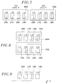
- each output channel 130, 140 is shown diagrammatically, 150 corresponding to the channels of FIG. 1, by a rectangle comprising a central separation in the form of a vertical line.
- each of these three channels has been represented twice.
- channel 150 is positioned at the output of the coupler 120 so as to receive a wavelength of 1.28 ⁇ m in the first free spectral range 600, and a wavelength of 1.44 ⁇ m in the second free spectral range 700.
- channel 140 is positioned to receive, in the first free spectral range 600, the wavelength 1.32 ⁇ m and, in the second free spectral range 700, the wavelength 1.48 ⁇ m.
- channel 130 is positioned so to receive, in the first free spectral interval 600, a wavelength 1.39 ⁇ m, and in the second free spectral range 700, a length 1.54 ⁇ m wave.
- the channels 130, 140 and 150 are, in FIG. 4, spaced from each other in proportion to the actual spacing they present between them at the output of the coupler 120.
- the signals transported through optical fiber 200 are only distributed over three wavelengths, the wavelengths 1.28, 1.32 and 1.54 ⁇ m. So the channel 130 has been crossed by a transverse line within the spectral interval free 600. Indeed, the receiver 300 connected to the second coupler by the channel 130, will only receive a signal of wavelength 1.54 ⁇ m, since none signal at 1.39 ⁇ m does not pass through the device as a whole. The length wave which it is able to convey within the first interval 600 is therefore unimportant.
- channels 140 and 150 since for each of these channels, one of the wavelengths that they are adapted to transmit does not take place inside the device of FIG. 1, and in particular, is not carried in fiber 200.
- each channel is placed in the coupler without taking into account that of a single free spectral interval, the free spectral interval having a central wavelength closest to that which this channel is intended for convey.
- channels 140 and 150 are placed taking into account only the central wavelength close to 1.3 ⁇ m, i.e. the arrangement of the first free spectral interval.
- channel 130 intended to convey a wavelength of 1.54 ⁇ m is placed in the coupler 120 taking into account only the value of the wavelength central of the second free spectral interval, that corresponding to wavelengths close to 1.5 ⁇ m.
- the channels 130, 140 and 150 are placed on an axis X with a spacing between them which is proportional to their spacing true within the output coupler 120. As can be seen on Figure 6, there is between the channels 140 and 150, a spacing substantially equal to the spacing between the channels 140 and 130.
- Channels 160 and 170 are placed in the output coupler 120 in knowing the exact central wavelength of the first interval free spectral 600, this central wavelength being close to 1.3 ⁇ m. Knowing this central wavelength, channel 160 is spaced from the center of coupler 120 by a distance corresponding to the difference of wavelengths between 1.28 ⁇ m and the central wavelength of the first free spectral interval 600. Likewise, channel 170 is placed at a distance from the center of the coupler 120 which corresponds to the difference between 1.32 ⁇ m and the central wavelength of the first free spectral range.
- channels 180 and 190 are placed at the outlet of the output coupler 120 at a distance from the center of output coupler 120 which is determined based on knowledge of the wavelength central of the second free spectral interval 700, so that these channels receive wavelengths equal to 1.51 ⁇ m and 1.55 ⁇ m.
- channels 160 and 170 are suitable for receiving, in the second free interval 700 this time, respective wavelengths 1.44 ⁇ m and 1.48 ⁇ m.
- the channels 180 and 190 are suitable for receiving, in the first free spectral interval 600, wavelengths of 1.36 and 1.40 ⁇ m, but do not transmit these wavelengths, because the signals transmitted through the optical fiber 200 do not contain signals to these wavelengths.
- FIG. 9 shows the four channels 160, 170, 180, 190 along an X axis representative of the positioning of the channels in the output coupler.
- the spacing between these channels in Figure 9 being proportional to the actual spacing between these channels at the output of the coupler output, we can see in Figure 9 that each time two channels consecutive have a substantially identical spacing.
- the phasar according to the invention is in practice capable of transmitting over each channel 160, 170, 180, 190 of the wavelength signals belonging to a narrow range of wavelengths surrounding the length waveform chosen for this channel. Placing two channels 180, 190 of so that one transmits signals around 1.51 ⁇ m, and the other transmits signals around 1.55 ⁇ m, allows to transmit on all of these two channels 180 and 190 all length signals wave located around 1.54 ⁇ m, and more precisely belonging to a window covering at least the range 1.51 - 1.55 ⁇ m.
- two channels 180, 190 of wavelengths respective 40 nm apart we have chosen, by example, two channels spaced 20 nm apart.
- a window extending around 1.54 ⁇ m is particularly useful when the phasar 100 is connected to a receiver 300 through the two channels 180 and 190, and where the phasar separates and transmits to this receiver 300, through these two channels 180 and 190, a multichannel signal, i.e. a signal composed of several signals having different wavelengths in the window around 1.54 ⁇ m.
- the signal separated by the phasar 100 can contain both a television signal and a signal carrying computer data.
- a phasar type separator device for example.
- an outlet channel consists of an epitaxial ribbon with a width of 2 ⁇ m.
- a conventional photolithography technique allows a minimum transverse separation between two edges adjacent consecutive guides which is equal to 0.85 ⁇ m. So a minimum transverse spatial separation between central axes of two outlet channels, is twice half a width of a guide added to the value of the minimum separation between edges of guides, i.e. 2.85 ⁇ m.
- the phasar 100 of FIGS. 1, 4, 5 and 6 includes a output coupler 120 whose output channels are positioned, by relation to the center of the coupler, at algebraic distances of -1.425 ⁇ m, 1.425 ⁇ m and 4.358 ⁇ m, respectively for the 1.28 ⁇ m, 1.32 ⁇ m channels and 1.54 ⁇ m. These positions are determined by considering that the light enters and leaves the coupler 110 through an input channel positioned at the center of this coupler 110.
- n a refractive index of the guides of the phasar network
- Dl is a constant length difference between two consecutive guides of the network.
- ⁇ 1 and ⁇ 2 are desired central wavelengths for the two free spectral intervals taking place in the output coupler, and where m 1 and m 2 are two different orders of interference, i.e. two different whole numbers.
- the equation m 1 / m 2 ⁇ 2 / ⁇ 1 must therefore be checked so that m 1 / m 2 must be close to 1.5 / 1.3.
- a known method for obtaining a good diaposopy is to adopt a difference in length between two consecutive network guides which is low. This is equivalent to adopting weak interference orders. So, we can, in the case of a classic phasar, adopt, for example, an order interference equal to 2 to reject additional adjacent lobes, to outside a wavelength region of the output coupler in increasing a wavelength width of the channels.
- Adopting a large number of guides allows, although the lobes adjacent secondaries are kept in the free spectral range, reduce the size of these side lobes.
- the invention proposes a geometric arrangement of the network of the phasar allowing to adopt a particularly high number of guides in the network.
- the scope of the invention is not limited to the case where only a good quality crosstalk is necessary.
- Such a provision of network guides prove to be particularly suitable whenever it is necessary or advantageous to adopt a large number of guides in the network, or to place guides according to a layout having a particularly small footprint.
- a phasar according to the invention turns out also particularly advantageous when it is necessary to carry out a network of guides with a difference in length between guides which is particularly weak, and constant.
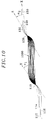
- FIG. 10 shows a phasar according to the invention, which corresponds to that of FIG. 1.
- the input coupler 110 has three input channels 112, 114 and 116, and the output coupler 120 has three output channels 130, 140 and 150. These three inputs are separated from these three outlets, via two free expansion zones acting as lenses, and a network of guides 1000. Only the entry guide 114 is used in the application described here.
- a phasar is proposed whose couplers, also symmetrical to each other, have respectively five input channels and five output channels. So if one of the guides is made unusable, another guide can be used to replace this unusable guide.
- the network 1000 has a wavy shape.
- a general axis X as an axis passing through the centers respective couplers 110 and 120, and two main directions are defined guides of the network 1000 in the vicinity respectively of the couplers 110 and 120.
- positive direction is defined by an arrow directed from the coupler 110 towards the coupler 120.
- the coupler 110 being arbitrarily defined as being the input coupler, the coupler 120 then being defined as the input coupler output, the positive direction of the Y axis of the input coupler 110 is defined as being the direction of departure of the guides of this input coupler 110.
- the positive direction of the Z axis of the output coupler 120 is defined as the direction of arrival of the guides on the output coupler 120.
- the angle ⁇ 1 is the oriented algebraic angle, defined according to the usual mathematical rules, starting from the general axis oriented X and going up to the axis oriented Y.
- the angle ⁇ 2 is the oriented algebraic angle, starting from the oriented axis X and going up to the oriented axis Z.
- angles ⁇ 1 and ⁇ 2 are of the same sign.
- the guides of the network emerge from the coupler 110 in a general direction Y oriented going upwards in FIG. 10 and the guides of the network emerge from the output coupler 120 in a direction going downwards.
- the couplers 110 and 120 are therefore inclined one upwards and the other downwards.
- the guides after emergence of the coupler 110, describe a first curvature so that their tangents pass an inclination rising in a horizontal direction at a central part of the network. In the central part of the network, the guides are straight and parallel to each other. Arriving near the coupler 120, the guides of the network again describe a curvature, this time a meaning curvature opposite the first bend, causing them to pass from an orientation horizontal again towards a rising orientation.
- each guide of the network 1000 describes a form of S and the device geometry is unchanged by 180 ° device rotation around a central axis of the device. Specifically, each guide in the network 1000 describes a first turn having a first direction of curvature, then a straight section, and finally a second turn with a second direction of curvature opposite to the first direction of curvature.
- Each guide of the network 1000 describes a curve of high curvature and a slight curve bend.
- the network guides arranged in low position in figure 10 are inside the first corner of the network and outside the second corner. They therefore have a small curvature in the first corner, and a strong curvature in the second corner.
- the guides arranged in the upper position of the network describe the first corner outside of it and the second corner inside this one.
- Such an arrangement of the network, and in particular of the couplers makes it possible on the one hand to place a very large number of guides in the network, on the other hand to be able to adopt particularly small length differences between the guides.
- An arrangement with couplers inclined with respect to the general axis X at respective angles ⁇ 1 , and ⁇ 2 equal thus makes it possible to have a particularly large number of guides having the same length.
- a slight difference between the two angles ⁇ 1 and ⁇ 2 makes it possible to obtain a network of guides in which the guides are longer as they are in the lower position in the network. While keeping a particularly small transverse space between two guides of the network, and with a particularly high number of guides, each difference in length Dl between consecutive guides corresponds to a difference ( ⁇ 2 - ⁇ 1 ) allowing this difference to be obtained of length Dl.
- the transverse spacing between two guides of the network can be chosen to be particularly low
- the phasar 100 according to the invention can include a large number of guides in this network without presenting too large a transverse volume in the central part of the network.
- FIG. 11 shows a variant of the phasar 100 according to the invention, in which the guides of the network 1000 further present an additional curvature in the central part of the network. More precisely, each guide presents, in addition to the first turn at in the vicinity of the coupler 110 and in addition to the turn in the vicinity of the coupler 120, an additional turn in the central part of the network, this turn having the same direction of curvature for each guide in the network 1000.
- the guides of the network 1000 emerge from each of the two couplers 110 and 120 and move apart from others to an area approximately every time at third of the length of the guides.
- the guides In the central bend, the guides have as much curvature stronger than they are outside the center bend. So the most along the network are the outer guides of the central turn.
- a first short turn at the coupler 110 compensates for a long turn at coupler 120, or conversely a long turn at the coupler 110 compensates for a turn short at the coupler 120.
- This type of geometry makes it possible to have a large number of guides in the network, for example 44 guides without overlap of these guides.
- FIG 11 there is shown an arrow E indicating the direction of increase in the wavelengths transmitted within channels 130, 140 and 150.
- the wavelength transmitted by a channel outlet is all the greater as this channel is located on the side of the interior of the central turn of the network 1000.
- the network 1000 has a length, measured between the two couplers 110 and 120, equal to 4000 ⁇ m.
- the networks of the devices of these two figures present a transverse width equal to 900 ⁇ m.
- FIG. 12 Represented in FIG. 12 are powers P detected on the output coupler output channels, for the second variant of the invention described with reference to Figures 7 to 9.
- Figure 12 is a graph on which the wavelengths ⁇ are plotted on the abscissa, in ⁇ m, and on the ordinate the powers P transmitted downstream of the phasar, in dB.
- the phasar 100 according to the invention has a dependence on the polarization of the light which is less than 2.5 nm on each channel.
- Figure 13 is also a graph showing the evolution of the power P detected by the phasar output channels of FIGS. 7 to 9, as a function of a wavelength ⁇ .
- Figure 13 differs from Figure 12 in that a portion of the curve corresponding to the power detected by channels 180 and 190 has been offset by a free spectral interval for easier comparison with two curves representing the powers detected by channels 160 and 170.
- Figure 14 represents the evolution of the crosstalk, or Crosstalk according to English terminology, in dB, as a function of a wavelength ⁇ . This crosstalk is better than -20dB.
- This structure is made on a semi-insulating 900 InP substrate, by depositing by epitaxy, several times on top of each other, identical sets 800 compounds each of two layers, one of InP having a thickness of 500 ⁇ and the other from InGaAsP having a thickness of 500 ⁇ and a length 1.17 ⁇ m band gap wave.
- This 800 set of two layers is for example repeated ten times.
- These layers have a structure chosen so as to be able to guide optical waves, both at a wavelength of 1.3 ⁇ m and at a 1.5 ⁇ m wavelength. These layers also have a structure their allowing to have the same behavior at these wavelengths, what whatever the polarization of the light.
- a ribbon is produced in accordance with that of FIG. 15 by putting in creates a unique reactive ion etching of these layers, based on a mixture of methane and hydrogen.
- this difference in length can be obtained by giving to the guides, each consisting for example of a stack in accordance with that of FIG. 15, an appropriate additional curvature in the central part of the network.
- Such a production method makes it possible to obtain length differences between consecutive guides particularly weak, impossible to obtain with the processes known until now.
- the phasar according to the invention can be produced by implementing polarization compensation processes, i.e. processes making it possible to reduce or make negligible a separation between TE and TM modes, this separation being conventionally 2.5 nm.
- polarization compensation processes i.e. processes making it possible to reduce or make negligible a separation between TE and TM modes, this separation being conventionally 2.5 nm.
- a wider wavelength response width allows better tolerance depending on both temperature variations and function of polarization.
- a large width of spectral response is advantageous, especially to cover the whole window at 1.54 ⁇ m, i.e. wavelengths ranging from 1.52 ⁇ m to 1.56 ⁇ m.
- wavelengths ranging from 1.52 ⁇ m to 1.56 ⁇ m.
- two channels one at 1.535 ⁇ m and the other at 1.55 ⁇ m, such a window ranging from 1.52 to 1.56 ⁇ m is fully covered.
Landscapes
- Physics & Mathematics (AREA)
- General Physics & Mathematics (AREA)
- Optics & Photonics (AREA)
- Engineering & Computer Science (AREA)
- Microelectronics & Electronic Packaging (AREA)
- Optical Communication System (AREA)
Applications Claiming Priority (2)
| Application Number | Priority Date | Filing Date | Title |
|---|---|---|---|
| FR9715477A FR2772144B1 (fr) | 1997-12-08 | 1997-12-08 | Dispositif d'echange de signaux optiques a travers une fibre optique |
| FR9715477 | 1997-12-08 |
Publications (1)
| Publication Number | Publication Date |
|---|---|
| EP0921424A1 true EP0921424A1 (de) | 1999-06-09 |
Family
ID=9514294
Family Applications (1)
| Application Number | Title | Priority Date | Filing Date |
|---|---|---|---|
| EP98403079A Withdrawn EP0921424A1 (de) | 1997-12-08 | 1998-12-08 | Vorrichtung zum Austausch von optischen Signalen durch eine optische Faser |
Country Status (3)
| Country | Link |
|---|---|
| US (1) | US6377379B1 (de) |
| EP (1) | EP0921424A1 (de) |
| FR (1) | FR2772144B1 (de) |
Families Citing this family (2)
| Publication number | Priority date | Publication date | Assignee | Title |
|---|---|---|---|---|
| JP3818169B2 (ja) * | 2002-02-22 | 2006-09-06 | 日本電気株式会社 | 導波路デバイス |
| US7447439B2 (en) * | 2004-05-07 | 2008-11-04 | Enablence Inc. | Optical duplexer and optical triplexer |
Citations (3)
| Publication number | Priority date | Publication date | Assignee | Title |
|---|---|---|---|---|
| US5212758A (en) * | 1992-04-10 | 1993-05-18 | At&T Bell Laboratories | Planar lens and low order array multiplexer |
| EP0651530A2 (de) * | 1993-11-03 | 1995-05-03 | AT&T Corp. | Kommunikationssysteme unter Verwendung passiver Hochfrequenzverkehrslenkung |
| EP0703473A1 (de) * | 1994-09-23 | 1996-03-27 | France Telecom | Optoelektronische Vorrichtung mit integriertem verbesserten Mehrfachwellenlängen-Empfänger |
Family Cites Families (4)
| Publication number | Priority date | Publication date | Assignee | Title |
|---|---|---|---|---|
| US5440416A (en) * | 1993-02-24 | 1995-08-08 | At&T Corp. | Optical network comprising a compact wavelength-dividing component |
| ES2160268T3 (es) * | 1996-01-25 | 2001-11-01 | Infineon Technologies Ag | Procedimiento para el funcionamiento de una red en fase. |
| US5999290A (en) * | 1997-10-27 | 1999-12-07 | Lucent Technologies Inc. | Optical add/drop multiplexer having complementary stages |
| FR2772143B1 (fr) * | 1997-12-08 | 2001-12-28 | France Telecom | Composant optique a spectrographe a reseau de guides, a geometrie de reseau amelioree |
-
1997
- 1997-12-08 FR FR9715477A patent/FR2772144B1/fr not_active Expired - Fee Related
-
1998
- 1998-12-08 EP EP98403079A patent/EP0921424A1/de not_active Withdrawn
- 1998-12-08 US US09/207,692 patent/US6377379B1/en not_active Expired - Fee Related
Patent Citations (3)
| Publication number | Priority date | Publication date | Assignee | Title |
|---|---|---|---|---|
| US5212758A (en) * | 1992-04-10 | 1993-05-18 | At&T Bell Laboratories | Planar lens and low order array multiplexer |
| EP0651530A2 (de) * | 1993-11-03 | 1995-05-03 | AT&T Corp. | Kommunikationssysteme unter Verwendung passiver Hochfrequenzverkehrslenkung |
| EP0703473A1 (de) * | 1994-09-23 | 1996-03-27 | France Telecom | Optoelektronische Vorrichtung mit integriertem verbesserten Mehrfachwellenlängen-Empfänger |
Non-Patent Citations (3)
| Title |
|---|
| "WAVELENGTH LOCKING SCHEME USING A GRATING DEMULTIPLEXER FOR APPLICATIONS IN WDMA NETWORKS AND WDM LINKS", IBM TECHNICAL DISCLOSURE BULLETIN, vol. 38, no. 5, 1 May 1995 (1995-05-01), pages 413 - 415, XP000519628 * |
| AMERSFOORT M R ET AL: "HIGH PERFORMANCE 4-CHANNEL PHASAR WAVELENGTH DEMULTIPLEXER INTEGRATED WITH PHOTODETECTORS", PROCEEDINGS OF THE EUROPEAN CONFERENCE ON OPTICAL COMMUNICATION (EC, MONTREUX, SEPT. 12 - 16, 1993, vol. VOL. 3, no. CONF. 19, 12 September 1993 (1993-09-12), SWISS ELECTROTECHNICAL ASSOCIATION, pages 49 - 52, XP000492285 * |
| MESTRIC R ET AL: "DESIGN AND FABRICATION OF 1.31-1.55-MUM PHASED-ARRAY DUPLEXER ON INP", IEEE JOURNAL OF SELECTED TOPICS IN QUANTUM ELECTRONICS, vol. 2, no. 2, June 1996 (1996-06-01), pages 251 - 256, XP000685237 * |
Also Published As
| Publication number | Publication date |
|---|---|
| US6377379B1 (en) | 2002-04-23 |
| FR2772144B1 (fr) | 2000-02-25 |
| FR2772144A1 (fr) | 1999-06-11 |
Similar Documents
| Publication | Publication Date | Title |
|---|---|---|
| EP2286289B1 (de) | Vorrichtung zum kuppeln einer glasfaser und einer nanophotonischen komponente | |
| EP3491438B1 (de) | Multispektraler optischer koppler mit niedrigen empfangsverlusten | |
| EP0005093B1 (de) | Optische integrierte Demultiplexieranordnung und Verfahren zu seiner Herstellung | |
| EP0196948A1 (de) | Umkehrbare Demultiplexeinrichtung von einer Mehrzahl von Lichtsignalen in integrierter Optik | |
| EP0851252A1 (de) | Temperaturunabhängiter optischer Multiplexer und/oder Demultiplexer | |
| EP2141520A1 (de) | Kupplungsvorrichtung mit kompensierter Doppelbrechung | |
| EP0869377B1 (de) | Integriertes optisches Bauelement mit Polarisationseffekt | |
| FR2477287A2 (fr) | Repartiteur optique multiple de la lumiere, procede de realisation d'un filtre interferentiel pour un tel repartiteur et mise en oeuvre de ce repartiteur | |
| EP1377857A2 (de) | Hochauflösende integrierte optische spektrometer und zugehöriges herstellungsverfahren | |
| FR2830346A1 (fr) | Modulateur electro-optique, procede de realisation et bloc pour mise en oeuvre | |
| EP0831346A1 (de) | Wellenleitergitter-Spektrograph als Multiplexer-Komponente | |
| CA2311157A1 (fr) | Multiplexeur/demultiplexeur optique a trois guides d'onde | |
| EP0916977A1 (de) | Demultiplexer mit quadratischer spektraler antwort | |
| EP0921423A1 (de) | Optische Komponente mit Wellenleiter-Gitter-Spektrograph mit verbesserter Gittergeometrie | |
| CA2160217C (fr) | Coupleur optique selectif en longueur d'onde | |
| EP0921422A1 (de) | Optische Komponente nach der Art eines Wellenleiter-Gitter- Spektrographes mit zentrierten Ausgangskanälen | |
| EP0921424A1 (de) | Vorrichtung zum Austausch von optischen Signalen durch eine optische Faser | |
| EP1494293A2 (de) | Photodetektor mit vertikalem Resonanzhohlraum, Anordnung und entsprechedes Telekommunikationssystem | |
| EP1516212A2 (de) | Optischer wellenlängenselektiver richtkoppler | |
| FR2794858A1 (fr) | Dispositif analyseur de spectre optique a reseau de diffraction en optique integree | |
| FR3025659A1 (fr) | Source laser multi-longueurs d'onde auto-alignee et emetteur-recepteur integrant une telle source | |
| FR2685786A1 (fr) | Coupleur de proximite en optique integree. | |
| WO2002075366A2 (fr) | Composant optique a base de fibre bi-coeur avec entrees/sorties en fibres mono-coeur | |
| Biswas et al. | A Review on Arrayed Waveguide Grating Multiplexer/De-multiplexer forDense Wavelength Division Multiplexing Systems | |
| FR2761485A1 (fr) | Multiplexeur-demultiplexeur en longueur d'onde a fibres optiques |
Legal Events
| Date | Code | Title | Description |
|---|---|---|---|
| PUAI | Public reference made under article 153(3) epc to a published international application that has entered the european phase |
Free format text: ORIGINAL CODE: 0009012 |
|
| AK | Designated contracting states |
Kind code of ref document: A1 Designated state(s): DE GB |
|
| AX | Request for extension of the european patent |
Free format text: AL;LT;LV;MK;RO;SI |
|
| 17P | Request for examination filed |
Effective date: 19991206 |
|
| AKX | Designation fees paid |
Free format text: DE GB |
|
| RAP1 | Party data changed (applicant data changed or rights of an application transferred) |
Owner name: ALCATEL |
|
| RAP1 | Party data changed (applicant data changed or rights of an application transferred) |
Owner name: AVANEX CORPORATION |
|
| 17Q | First examination report despatched |
Effective date: 20041105 |
|
| STAA | Information on the status of an ep patent application or granted ep patent |
Free format text: STATUS: THE APPLICATION IS DEEMED TO BE WITHDRAWN |
|
| 18D | Application deemed to be withdrawn |
Effective date: 20050316 |