EP0196948A1 - Umkehrbare Demultiplexeinrichtung von einer Mehrzahl von Lichtsignalen in integrierter Optik - Google Patents
Umkehrbare Demultiplexeinrichtung von einer Mehrzahl von Lichtsignalen in integrierter Optik Download PDFInfo
- Publication number
- EP0196948A1 EP0196948A1 EP86400499A EP86400499A EP0196948A1 EP 0196948 A1 EP0196948 A1 EP 0196948A1 EP 86400499 A EP86400499 A EP 86400499A EP 86400499 A EP86400499 A EP 86400499A EP 0196948 A1 EP0196948 A1 EP 0196948A1
- Authority
- EP
- European Patent Office
- Prior art keywords
- light
- layer
- guide
- light beam
- light signals
- Prior art date
- Legal status (The legal status is an assumption and is not a legal conclusion. Google has not performed a legal analysis and makes no representation as to the accuracy of the status listed.)
- Granted
Links
- 230000002441 reversible effect Effects 0.000 title claims abstract description 7
- 239000013307 optical fiber Substances 0.000 claims abstract description 53
- VYPSYNLAJGMNEJ-UHFFFAOYSA-N Silicium dioxide Chemical compound O=[Si]=O VYPSYNLAJGMNEJ-UHFFFAOYSA-N 0.000 claims description 36
- 229910052814 silicon oxide Inorganic materials 0.000 claims description 29
- 230000003287 optical effect Effects 0.000 claims description 20
- 239000000758 substrate Substances 0.000 claims description 17
- 238000005530 etching Methods 0.000 claims description 13
- XUIMIQQOPSSXEZ-UHFFFAOYSA-N Silicon Chemical compound [Si] XUIMIQQOPSSXEZ-UHFFFAOYSA-N 0.000 claims description 12
- 229910052710 silicon Inorganic materials 0.000 claims description 12
- 239000010703 silicon Substances 0.000 claims description 12
- 239000000463 material Substances 0.000 claims description 6
- OAICVXFJPJFONN-UHFFFAOYSA-N Phosphorus Chemical compound [P] OAICVXFJPJFONN-UHFFFAOYSA-N 0.000 claims description 5
- 229910052698 phosphorus Inorganic materials 0.000 claims description 5
- 239000011574 phosphorus Substances 0.000 claims description 5
- 239000004065 semiconductor Substances 0.000 claims description 5
- RTAQQCXQSZGOHL-UHFFFAOYSA-N Titanium Chemical compound [Ti] RTAQQCXQSZGOHL-UHFFFAOYSA-N 0.000 claims description 4
- 229910052732 germanium Inorganic materials 0.000 claims description 4
- GNPVGFCGXDBREM-UHFFFAOYSA-N germanium atom Chemical compound [Ge] GNPVGFCGXDBREM-UHFFFAOYSA-N 0.000 claims description 4
- 229910052719 titanium Inorganic materials 0.000 claims description 4
- 239000010936 titanium Substances 0.000 claims description 4
- 229910052581 Si3N4 Inorganic materials 0.000 claims description 3
- HQVNEWCFYHHQES-UHFFFAOYSA-N silicon nitride Chemical compound N12[Si]34N5[Si]62N3[Si]51N64 HQVNEWCFYHHQES-UHFFFAOYSA-N 0.000 claims description 3
- 238000000034 method Methods 0.000 description 9
- 230000008878 coupling Effects 0.000 description 8
- 238000010168 coupling process Methods 0.000 description 8
- 238000005859 coupling reaction Methods 0.000 description 8
- 238000005229 chemical vapour deposition Methods 0.000 description 7
- 239000000835 fiber Substances 0.000 description 5
- ZOXJGFHDIHLPTG-UHFFFAOYSA-N Boron Chemical compound [B] ZOXJGFHDIHLPTG-UHFFFAOYSA-N 0.000 description 3
- PXGOKWXKJXAPGV-UHFFFAOYSA-N Fluorine Chemical compound FF PXGOKWXKJXAPGV-UHFFFAOYSA-N 0.000 description 3
- 229910052796 boron Inorganic materials 0.000 description 3
- 238000000151 deposition Methods 0.000 description 3
- 229910052731 fluorine Inorganic materials 0.000 description 3
- 239000011737 fluorine Substances 0.000 description 3
- 238000001020 plasma etching Methods 0.000 description 3
- 239000000377 silicon dioxide Substances 0.000 description 3
- 239000003795 chemical substances by application Substances 0.000 description 2
- 230000008021 deposition Effects 0.000 description 2
- 235000021183 entrée Nutrition 0.000 description 2
- 238000004519 manufacturing process Methods 0.000 description 2
- 230000003647 oxidation Effects 0.000 description 2
- 238000007254 oxidation reaction Methods 0.000 description 2
- 238000000206 photolithography Methods 0.000 description 2
- 229910001218 Gallium arsenide Inorganic materials 0.000 description 1
- 238000003491 array Methods 0.000 description 1
- 230000005540 biological transmission Effects 0.000 description 1
- 238000003776 cleavage reaction Methods 0.000 description 1
- 230000007423 decrease Effects 0.000 description 1
- 239000006185 dispersion Substances 0.000 description 1
- 239000002019 doping agent Substances 0.000 description 1
- 238000005516 engineering process Methods 0.000 description 1
- -1 glass Chemical compound 0.000 description 1
- 239000011521 glass Substances 0.000 description 1
- 238000012986 modification Methods 0.000 description 1
- 230000004048 modification Effects 0.000 description 1
- 229910021421 monocrystalline silicon Inorganic materials 0.000 description 1
- 150000004767 nitrides Chemical class 0.000 description 1
- 230000000737 periodic effect Effects 0.000 description 1
- 230000007017 scission Effects 0.000 description 1
- 238000000926 separation method Methods 0.000 description 1
- TXEYQDLBPFQVAA-UHFFFAOYSA-N tetrafluoromethane Chemical compound FC(F)(F)F TXEYQDLBPFQVAA-UHFFFAOYSA-N 0.000 description 1
Images


Classifications
-
- G—PHYSICS
- G02—OPTICS
- G02B—OPTICAL ELEMENTS, SYSTEMS OR APPARATUS
- G02B6/00—Light guides; Structural details of arrangements comprising light guides and other optical elements, e.g. couplings
- G02B6/10—Light guides; Structural details of arrangements comprising light guides and other optical elements, e.g. couplings of the optical waveguide type
- G02B6/12—Light guides; Structural details of arrangements comprising light guides and other optical elements, e.g. couplings of the optical waveguide type of the integrated circuit kind
- G02B6/12007—Light guides; Structural details of arrangements comprising light guides and other optical elements, e.g. couplings of the optical waveguide type of the integrated circuit kind forming wavelength selective elements, e.g. multiplexer, demultiplexer
-
- G—PHYSICS
- G02—OPTICS
- G02B—OPTICAL ELEMENTS, SYSTEMS OR APPARATUS
- G02B6/00—Light guides; Structural details of arrangements comprising light guides and other optical elements, e.g. couplings
- G02B6/10—Light guides; Structural details of arrangements comprising light guides and other optical elements, e.g. couplings of the optical waveguide type
- G02B6/12—Light guides; Structural details of arrangements comprising light guides and other optical elements, e.g. couplings of the optical waveguide type of the integrated circuit kind
- G02B6/12004—Combinations of two or more optical elements
-
- G—PHYSICS
- G02—OPTICS
- G02B—OPTICAL ELEMENTS, SYSTEMS OR APPARATUS
- G02B6/00—Light guides; Structural details of arrangements comprising light guides and other optical elements, e.g. couplings
- G02B6/10—Light guides; Structural details of arrangements comprising light guides and other optical elements, e.g. couplings of the optical waveguide type
- G02B6/12—Light guides; Structural details of arrangements comprising light guides and other optical elements, e.g. couplings of the optical waveguide type of the integrated circuit kind
- G02B6/122—Basic optical elements, e.g. light-guiding paths
- G02B6/124—Geodesic lenses or integrated gratings
-
- G—PHYSICS
- G02—OPTICS
- G02B—OPTICAL ELEMENTS, SYSTEMS OR APPARATUS
- G02B6/00—Light guides; Structural details of arrangements comprising light guides and other optical elements, e.g. couplings
- G02B6/24—Coupling light guides
- G02B6/26—Optical coupling means
- G02B6/28—Optical coupling means having data bus means, i.e. plural waveguides interconnected and providing an inherently bidirectional system by mixing and splitting signals
- G02B6/293—Optical coupling means having data bus means, i.e. plural waveguides interconnected and providing an inherently bidirectional system by mixing and splitting signals with wavelength selective means
- G02B6/29304—Optical coupling means having data bus means, i.e. plural waveguides interconnected and providing an inherently bidirectional system by mixing and splitting signals with wavelength selective means operating by diffraction, e.g. grating
- G02B6/29316—Light guides comprising a diffractive element, e.g. grating in or on the light guide such that diffracted light is confined in the light guide
- G02B6/29325—Light guides comprising a diffractive element, e.g. grating in or on the light guide such that diffracted light is confined in the light guide of the slab or planar or plate like form, i.e. confinement in a single transverse dimension only
-
- G—PHYSICS
- G02—OPTICS
- G02B—OPTICAL ELEMENTS, SYSTEMS OR APPARATUS
- G02B6/00—Light guides; Structural details of arrangements comprising light guides and other optical elements, e.g. couplings
- G02B6/24—Coupling light guides
- G02B6/26—Optical coupling means
- G02B6/28—Optical coupling means having data bus means, i.e. plural waveguides interconnected and providing an inherently bidirectional system by mixing and splitting signals
- G02B6/293—Optical coupling means having data bus means, i.e. plural waveguides interconnected and providing an inherently bidirectional system by mixing and splitting signals with wavelength selective means
- G02B6/29379—Optical coupling means having data bus means, i.e. plural waveguides interconnected and providing an inherently bidirectional system by mixing and splitting signals with wavelength selective means characterised by the function or use of the complete device
- G02B6/2938—Optical coupling means having data bus means, i.e. plural waveguides interconnected and providing an inherently bidirectional system by mixing and splitting signals with wavelength selective means characterised by the function or use of the complete device for multiplexing or demultiplexing, i.e. combining or separating wavelengths, e.g. 1xN, NxM
Definitions
- the present invention relates to a device for multiplexing or demultiplexing several light signals in integrated optics. It finds an application in particular in the fields of radar signal processing in real time, optical telecommunications, fiber optic sensors, etc.
- a demutfiplexing device or a demultiplexer, in integrated optics is a device which makes it possible to separate n light signals of different wavelengths transported by the same first optical fiber and to reinject 0respectively into n second optical fibers said n signals.
- a multiplexing or multiplexer device is a device which makes it possible to group together in a single beam, n light signals of different wavelengths originating respectively from n optical fibers.
- the ideal multiplexing element is therefore a niche filter, of width ⁇ ⁇ / 2 and of transmission 1 if ⁇ i - ⁇ / 2 ⁇ ⁇ i + ⁇ / 2, which would reflect or on the contrary perfectly transmit the light signals whose lengths wavelengths are not included in this interval and conversely would transmit or reflect those whose wavelengths are included in this interval.
- a succession of such filters would constitute an ideal multiplexing device.
- the second important problem is the coupling of the multiplexing device with the generally single-mode optical fibers, transporting the light information.
- the light losses at the input and at the output of the multiplexing device must be as low as possible.
- the multiplexer function that is to say the chromatic dispersion of the different light signals is provided by a network, as in conventional optics.
- a multiplexing device is described in particular in an article by Applied Optics, vol. 21, n ° 12, of June 15, 1982, pages 2195 to 2198 of T. SUHARA et al. titled "Integrated-Optc wavelength multi-and demultplexers using a chirped grating and an ion-exchanged waveguide".
- multiplexing devices do not solve the most important problem concerning the coupling of the multiplexer and the single-mode optical fibers used for the transport of light information as well as that of the collimation of the light beam which attacks the dispersive or network element of the device. multiplexing.
- the subject of the present invention is precisely a device for reversible demultiplexing of several light signals in integrated optics making it possible to remedy the various drawbacks given above.
- it allows good coupling with the optical fibers used for transporting information and therefore low light losses.
- the multiplexing of several light signals of different wavelengths allows, more easily than the devices of the prior art, the multiplexing of several light signals of different wavelengths, for example up to eight signals, while retaining acceptable total light losses.
- the multiplexing or multiplexing device of the invention can be produced according to a perfectly reproducible technology.
- the device according to the invention is reversible, that is to say it allows either demultiplexing or multiplexing of light signals.
- the device In the multiplexing direction, the device is used to inject an outgoing light beam into the first fiber, containing n light signals originating respectively from n second optical fibers.
- the input optics plays the role of output optics; the arrays are used to combine two light beams and the n output optics play the role of n input optics.
- the achromatic input optic which is advantageously a parabolic mirror, collimates the light beam to be processed in the multiplexing device. It thus allows networks to work in the Bragg regime and therefore to ensure good wavelength selection.
- the part carrying only one of the n light signals is the part of the light beam diffracted by the corresponding network
- the device according to the invention comprises an input microguide, interposed between the first optical fiber and the input optic, having a structure close to that of the first optical fiber and or output microguides, interposed respectively between the n output optics and the n second optical fibers, respectively having a structure close to that of the second optical fibers.
- the use of an input microguide and of n output microguides having a structure very close to that of the input and output optical fibers respectively, makes it possible to ensure good coupling between these fibers and the multiplexing device, thus limiting the light losses at the entry and exit of the device.
- the output microguides of the multiplexing device are curved.
- the output optics of this device are achromatic parabolic mirrors; these mirrors allow good focusing of the light beams entering the different second optical fibers respectively.
- the optical components are formed in two superimposed light guides, a lower guide with large index variation and an upper guide with small index variation in which propagates the incident light beam.
- the multiplexing device comprises n first gratings each serving to diffract a first part of the light beam and to transmit a second part of said light beam, one of the two parts carrying only one of the n light signals, the other part, transporting the other light signals, being sent in the direction of the first following network, the part transporting only one of the n light signals then being transferred from the upper guide to the lower guide, as well as n second networks associated with said first each serving to retransfer the part of the light beam carrying only one of the n light signals from the lower guide to the upper guide.
- the optical elements of the multiplexing device are formed by etching at least part of the light guide.
- the light guide comprises, produced in order on a silicon substrate, a first layer of undoped silicon oxide, a second layer of silicon oxide doped and a third layer of silicon oxide optionally doped with an element reducing the refractive index of this third layer, the doping of the material of the second layer being such that its refractive index is greater than that of the first and third layers .
- the two light guides comprise, produced in order on a semiconductor substrate, in particular made of silicon, a first layer, for example of undoped silicon oxide, a second layer in particular of silicon nitride, a third layer for example of doped silicon oxide and a fourth layer in particular of silicon oxide optionally doped with an element reducing the refractive index of this fourth layer, the third layer being such that its refractive index is higher than that of the first and fourth layers and lower than that of the second layer, the first, second and third layers forming the lower light guide and the first, third and fourth layers forming the upper light guide.
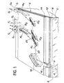
- FIGs 1 and 2 there is shown - schematically an integrated multiplexing device according to the invention used to separate n light signals, respectively of wavelengths X ,, ⁇ 2 , ..., X n , transported by a first optical fiber 2, in particular made of silica, and to be injected respectively into n second optical fibers F ,, F., ... Fn, the n light signals.
- the optical fiber F receives only the light signal of wavelength ⁇ 1
- the optical fiber F n receives only the light signal of wavelength X n .
- the wavelengths X ,, ⁇ 2 , ..., X n can be between 0.7 ⁇ m and 1.8 ⁇ m.
- the n light signals transported by the first optical fiber 2 form a single incident light beam 4.
- This multiplexing device comprises, as shown in FIG. 1, a light guide 6 produced on a monocrystalline semiconductor substrate 8, for example made of silicon or formed of III-V material such as GaAs.
- the substrate is obtained by cleavage of a semiconductor block in order to present strictly parallel faces E and S.
- the light guide 6 consists of three superimposed layers 10, 12 and 14 respectively.
- the layer 12, interposed between the layers 10 and the layer 14, constitutes the guide layer of the guide. It has a higher refractive index than that of layers 10 and 14.
- the lower layer 10 surmounting the substrate 8 is made of pure silicon oxide, the layer 12 of silicon oxide doped in particular with phosphorus, germanium or titanium, and the upper layer 14 made of pure silicon oxide or doped with an element such as boron or fluorine, reducing the refractive index of said layer.
- the layers of pure oxide 1 0 and 14 have, for the same length of approximately 0.8 ⁇ m, a refractive index for example of 1.45 for pure oxide and the doped oxide layer 12 an index 1.46.
- This light guide with low index variation has characteristics close to those of single-mode silica optical fibers generally used in integrated optics; its low index variation makes it possible to remain monomode even for a guiding layer 12 of 10 ⁇ m.
- the multiplexing device comprises at its input E a microguide 16, making it possible to ensure good coupling between the first optical fiber 2 transporting the light signals of different wavelengths and the multiplexing device.
- This input microguide 16 has a structure very similar to that constituting the optical fiber 2 which is in particular a single-mode fiber made of silica or silicon oxide.
- This microguide 16, as shown in FIG. 2, is preferably a rectilinear microguide.
- Achromatic optics 18 such as an achromatic mirror of parabolic shape makes it possible to collimate the light beam 4, coming from the input microguide 16 and containing the light signals of different wavelengths.
- this optic 18 makes it possible to transform, as shown in FIG. 3, the light leaving the microguide 16 assimilated to a light point P into a parallel light beam 20; to do this, the light point P must be located at the focal point of the optics 18.
- These networks are periodic structures; they comprise, in the form of regularly spaced parallel strips, an alternation of hollows and bumps (FIG. 4a).
- the first grating R 1 makes it possible, for example, to diffract the part of the light beam 22 transporting the light signal having the wavelength ⁇ 1 , and to transmit the rest 24 of the light beam, containing the other light signals.
- Part 24 of the incident beam 20 transmitted by the first network R is received by the second network R 2 -
- the latter in turn diffracts part 26 of the light beam 24 containing the optical signal of wavelength ⁇ 2 and transmits the remainder 28 of the light signal 24, on the third network R 3 .
- the n light signals of different wavelengths respectively ⁇ 1 , ⁇ 2 , ..., ⁇ n are separated from each other and sent to the optical fibers F 1 , F 2 , ..., F n corresponding.
- the Bragg or attack angle ⁇ i of the network R i i being an integer ranging from 1 to n, identified with respect to the normal to said network, is chosen according to the possibilities of technological realization of the structure of the different networks .
- This angle ⁇ i depends on the wavelength ⁇ i to be diffracted as well as on the pitch of the corresponding network p i
- the ith network R i can be determined so that it reflects the wavelength ⁇ i and transmits others.
- ⁇ i 2pisin ⁇ i-
- This condition can be realized by choosing the pitch p i of the network R i and by varying ⁇ i to make the selection in wavelength or else keep ⁇ i constant and make vary the network pitch pi.
- the diffracted light beams such as 22 and 26, are no longer strictly parallel beams.
- the diffracted light beams such as 22 and 26 are no longer strictly parallel beams.
- n elements optics M 1 , M 2 , ..., M n are provided for focusing the light beams diffracted by the various gratings.
- Each mirror M i is associated with a network R i and it makes it possible to focus the part of the light beam diffracted by this network R i .
- each microguide G i has a structure very close to the corresponding optical fiber F i receiving the light signal of wavelength ⁇ i -.
- the focal points of the optical elements M ,, M 2 , ..., M n are located just at the entrance of the microguides G 1 , G 2 , ..., G n correspondents.
- these microguides have a curved shape, which contributes to bringing out the different light signals diffracted by the networks R ,, R 2 , ..., R n , respectively transporting the light signal ⁇ 1 , ⁇ 2 , .. ., ⁇ n, perpendicular to the cleaved face S of the monocrystalline substrate 8 of silicon.
- the first step consists in growing by thermal oxidation of the substrate the lower layer 10 of silicon oxide ranging from 1 to 5 ⁇ m thick. This growth can be obtained at low temperature between 800 and 850 ° C and under a pressure of about 10 6 Pa or at higher temperature between 1000 ° C and 1150 ° C under atmospheric pressure.
- the layer 12 of silicon oxide 3 doped with phosphorus, germanium or titanium is deposited by a chemical vapor deposition process, assisted or not by plasma.
- This doped silicon oxide layer has a thickness ranging from 4 to 10 ⁇ m.
- the amount of dopant introduced for example from 10 21 to 10 22 atoms / cm 3 for phosphorus, it is possible to adapt the difference in index between the doped layer 12 and the lower layers 1 0 and upper 14 ; a difference 10- 3 index may be sufficient.
- the third layer of silicon oxide can be deposited by a chemical vapor deposition process assisted or not by plasma.
- This layer 14 can be made of pure oxide or doped with an element which decreases the refractive index of this layer, such as as boron or fluorine
- This upper layer represents a thickness ranging from 1 to 6 ⁇ m.
- the following steps consist in etching the light guide thus produced, through an appropriate mask, according to conventional photolithography methods, so as to form the various optical components.
- an anisotropic etching such as, for example, reactive ion etching using as an attack agent carbon tetrafluoride or trifiuouroethane.
- the networks R ,, R 2 , ..., Rn it is possible to eliminate, as shown in FIG. 4a, at the locations provided for said networks, the upper layer 14 of the light guide and partially the guiding layer 12
- the depth of the etched grooves h is determined by the desired bandwidth ⁇ which depends on the strength of the network. The greater the depth h, the finer the selection in wavelength ( ⁇ ).
- the deposition of the lower layer 10 and of the guiding layer 12 of the light guide is carried out, according to the same deposition techniques. Then, using an appropriate mask, defined according to conventional photolithography methods, the guiding layer 12, as shown in FIG. 4b, in order to form the different networks.
- This etching is in particular an anisotropic etching like a reactive ion etching.
- a layer of pure silicon oxide is deposited over the entire structure, the thickness of which corresponds to that of the upper layer 14 of the light guide.
- This deposition can be carried out by a chemical vapor deposition process assisted by plasma.
- the other optical elements are produced as before by etching one or more layers of the light guide.
- FIG 5 there is shown in perspective another embodiment of the multiplexing device according to the invention.
- the optical elements of this device playing the same roles as those described above, with reference to Figures 1 and 2, will bear the same references followed by an index a or a symbol '.
- This multiplexing device makes it possible to separate n light signals of wavelength ⁇ 1 , ⁇ 2 , ..., ⁇ n transported by the optical fiber 2 and to reinject them respectively into the n second optical fibers F 1 , F 2 , ..., F n .
- This device comprises two superimposed light guides 6a, a lower guide with large index variation and an upper guide with small index variation.
- These two superimposed light guides 6a are produced on a monocrystalline semiconductor substrate 8a in particular made of silicon and consist of a stack of four layers respectively bearing the references 10a, 11, 12a, 14a.
- the middle layers 11 and 12a correspond respectively to the guiding layers of the lower guide and the upper guide.
- the layer 1 1 has a higher refractive index than that of the layers 10a and 12a forming part of the lower guide and the layer 12a has a higher refractive index than that of the layer 10a and of the layer 14a forming the component upper light guide.
- the layer 10a can be made of undoped silicon oxide, obtained for example by thermal oxidation of the substrate at 800-850 ° C under 10 6 Pa or at higher temperature, between 1000 ° C and 1150 ° C under atmospheric pressure; it has such a refractive index of about 1.58 for a 0.8 micron wavelength and a thickness of 1 to 5 microns
- Layer 1 1 is advantageously made of silicon nitride material having a high refractive index, of the order of 2 for the same length.
- This layer can be deposited for example on layer 10a by a chemical vapor deposition process assisted or not by plasma. In particular, it has a thickness ranging from 0.01 ⁇ m to 0.2 ⁇ m.
- the layer 12a can be made of silicon oxide doped in particular with phosphorus, germanium or titanium. It has a refractive index slightly higher than that of the layer 10a (upper few 10- 3) and a thickness of 2 to 10 .mu.m. It can be deposited on layer 11, for example by a chemical vapor deposition process, assisted or not by plasma.
- the upper layer 14a can also be a layer of pure silicon oxide or doped with elements reducing the refractive index of said layer, such as boron or fluorine. It can also be formed by a chemical vapor deposition process, assisted or not by plasma. It has a refractive index of the order of 1.4 4 for a wavelength of 0.8 ⁇ m, and a thickness ranging from 1 to 6 ⁇ m.
- the upper guide with a small difference in index, a difference in index of 10 -3 being sufficient between the guiding layer and the adjacent layers, ensures good coupling with the optical fiber 2 transporting the different signals to be separated and with the optical fibers output of these different signals respectively F 1 , F 2 , ..., F n .
- This upper guide is a single-mode guide like the optical fibers 2 and F i , even for a guide layer 12a of 10 ⁇ m.
- the incident light beam 4 is transported in the multiplexing device by the upper guide of the device.
- the lower guide with large index variation offers a greater possibility of processing light signals than the guide with small index variation. Indeed, it is easy to produce in the guiding layer 11 of high index (Si 3 , N 4 ) optical components such as lenses, polarizers, etc., while these elements are practically impossible to produce in the layer guiding 12a of low index.
- This multiplexing device comprises, as before, an input microguide 16a, for example rectilinear, of the same structure as the optical fiber 2 making it possible to limit the light losses at the input of the multiplexing device, an achromatic input optic 18a such as a parabolic mirror used to make the light beam leaving the microguide 16a parallel as well as n first networks R ' 1 , R ' 2 , ..., R ' n arranged in cascade, working in Bra gg regime .
- an input microguide 16a for example rectilinear
- an achromatic input optic 18a such as a parabolic mirror used to make the light beam leaving the microguide 16a parallel as well as n first networks R ' 1 , R ' 2 , ..., R ' n arranged in cascade, working in Bra gg regime .
- each network R ′ 1 i going from 1 to n, serves for example to diffract the part of the light beam transporting the light signal of wavelength ⁇ i and to transmit the remainder of the light beam towards the following network R ' 1 + 1 .
- These networks R ' 1 , R ' 2 , ..., R ' n are calculated to couple the mode of the upper guide with the mode of the lower guide. They therefore make it possible, in addition to the wavelength selection, to transfer the light beam diffracted by them from the upper guide to the lower guide and more exactly from the guiding layer 12a of doped silicon oxide to the guiding layer 1 of nitride of silicon.
- the light beams respectively reflected by the networks T ,, T 2 , ..., T n are then respectively focused by means of optical elements M ' 1 , M ' 2 , ..., M such as parabolic achromatic mirrors, on the second optical fibers F 1 , F 2 , ..., Fntransporting the light signals of wavelength ⁇ 1 , ⁇ 2 , ..., ⁇ n respectively .
- Output microguides G ' 1 G 2 , ..., G ' n , curves respectively, can advantageously be interposed between the optics M ' 1 , M ' 2 , ..., M ' n and the optical fibers F, , F 2 , ..., F n to promote the coupling of the multiplexing device and said optical fibers F 1 , F 2 , ..., F n .
- the output mirrors MM ' 2 , ..., M n and the output microguides G ' 1 G 2, ..., G ' n allow the diffracted light beams to exit, each carrying a single signal, perpendicular to a cleaved face of the substrate.
- the angles of attack or Bragg angles of the networks R ' 1 , R ' 2 , ..., R ' n and of the networks T ,, T 2 , ..., T n are determined according to the effective index two guides in which the different optical elements of the multiplexing device are made; these effective indices depend on the thickness and the refractive index of the layers constituting the guides.
- the different optical elements of this multiplexing device can be produced, as before, by partially etching by means of reactive ion etching the layers of the two guides with CHF 3 or CF 4 as an attack agent.
- the microguides 16a and G can be obtained by only etching the upper layer 14a, 18a mirrors and M '1 by etching the four layers 14a, 12a, 11 and 10a and the networks R' 1 and T '1 by etching the upper layer 14a and partially layer 12a ( Figure 4a).
- the device of the invention allows the separation of up to eight light signals of different wavelengths while retaining acceptable total light losses, which was not possible with the multiplexing devices of the prior art.
- the parabolic mirrors located at the entrance or at the exit of the multiplexing device, can be produced by engraving only one or two layers of the light guides.
- the various networks can be produced by only engraving the upper layer of the light guides or else by engraving the three layers of said guides.
- microguides can be obtained by etching the doped silicon oxide layer 12 or 12a and then covering the assembly with the upper oxide layer.
- the thickness and the nature of the different layers of the light guides can be modified provided, however, that the guide layer has a refractive index slightly higher than that of the two adjacent layers of the corresponding guide and that this layer constitutes a guide layer. single mode.
- the substrate can be made of a material other than silicon such as glass, the first layer of silicon oxide then being obtained by chemical vapor deposition.
- the various gratings have been described as diffracting the part of the light beam carrying only one of the light signals and transmitting the part of the light beam containing the other signals.
- gratings transmitting the part of the light beam containing only one of the light signals and diffracting the part of said beam containing all the other signals.
- the device of the invention has been described for demultiplexing light signals, that is to say for separating signals from each other but of course, this device can also be used to multiplex these same signals, it that is to say to form from n light signals of different wavelengths a single light signal carrying these signals.
- This reversibility of the device of the invention is mainly linked to the use of parabolic achromatic mirrors 18, M ,, ..., M n .
- each mirror M i or M ' i is used to transform the incident beam of wavelength ⁇ i into a parallel beam and the mirror 18 or 18a is used to focus the resulting beam, coming from the network R 1 , containing the n light signals.
Landscapes
- Physics & Mathematics (AREA)
- General Physics & Mathematics (AREA)
- Optics & Photonics (AREA)
- Engineering & Computer Science (AREA)
- Microelectronics & Electronic Packaging (AREA)
- Optical Integrated Circuits (AREA)
- Optical Communication System (AREA)
Applications Claiming Priority (2)
| Application Number | Priority Date | Filing Date | Title |
|---|---|---|---|
| FR8503681 | 1985-03-13 | ||
| FR8503681A FR2579044B1 (fr) | 1985-03-13 | 1985-03-13 | Dispositif de multiplexage de plusieurs signaux lumineux en optique integree |
Publications (2)
| Publication Number | Publication Date |
|---|---|
| EP0196948A1 true EP0196948A1 (de) | 1986-10-08 |
| EP0196948B1 EP0196948B1 (de) | 1990-10-03 |
Family
ID=9317145
Family Applications (1)
| Application Number | Title | Priority Date | Filing Date |
|---|---|---|---|
| EP86400499A Expired - Lifetime EP0196948B1 (de) | 1985-03-13 | 1986-03-10 | Umkehrbare Demultiplexeinrichtung von einer Mehrzahl von Lichtsignalen in integrierter Optik |
Country Status (5)
| Country | Link |
|---|---|
| US (1) | US4740951A (de) |
| EP (1) | EP0196948B1 (de) |
| JP (1) | JPS61212805A (de) |
| DE (1) | DE3674615D1 (de) |
| FR (1) | FR2579044B1 (de) |
Cited By (13)
| Publication number | Priority date | Publication date | Assignee | Title |
|---|---|---|---|---|
| US4747655A (en) * | 1986-01-30 | 1988-05-31 | Fujitsu Limited | Optical wavelength compounding/dividing device |
| EP0340043A1 (de) * | 1988-04-29 | 1989-11-02 | Bt&D Technologies Limited | Optischer Wanderwellen-Modulator |
| FR2635198A1 (fr) * | 1988-08-03 | 1990-02-09 | Commissariat Energie Atomique | Dispositif de commutation de faisceaux lumineux integre |
| EP0365125A3 (de) * | 1988-09-17 | 1990-10-10 | Nortel Networks Corporation | Beugungsgitter |
| EP0359166A3 (de) * | 1988-09-15 | 1991-02-06 | Firma Carl Zeiss | Verfahren zum Herstellen von abbildenden optischen Elementen in planaren Wellenleitern |
| EP0390416A3 (de) * | 1989-03-28 | 1991-09-11 | AT&T Corp. | Optischer Multiplexer/Demultiplexer mit fokussierenden Bragg-Reflektoren |
| FR2660440A1 (fr) * | 1990-04-03 | 1991-10-04 | Commissariat Energie Atomique | Composant optique integre protege contre l'environnement et son procede de fabrication. |
| FR2689349A1 (fr) * | 1992-03-31 | 1993-10-01 | Alcatel Nv | Multiplexeur en longueur d'onde pour système optique intégré. |
| WO1997036198A1 (en) * | 1996-03-27 | 1997-10-02 | British Telecommunications Public Limited Company | Optical diffraction grating |
| WO1998030925A3 (en) * | 1996-12-20 | 1999-03-04 | Corning Inc | Reflective coupling array for optical waveguide |
| EP1004907A3 (de) * | 1998-11-24 | 2002-07-17 | Agilent Technologies, Inc. (a Delaware corporation) | Optischer Wellenlängen-Demultiplexer |
| EP2002296A4 (de) * | 2006-03-31 | 2009-06-03 | Enablence Inc | Planarer lichtfilter mit gemischten diffraktionselementen |
| EP2959503A4 (de) * | 2013-02-22 | 2016-10-26 | Kla Tencor Corp | Systeme zur bereitstellung von beleuchtung in der optischer messtechnik |
Families Citing this family (105)
| Publication number | Priority date | Publication date | Assignee | Title |
|---|---|---|---|---|
| DE3611246A1 (de) * | 1986-04-04 | 1987-10-15 | Kernforschungsz Karlsruhe | Verfahren zum herstellen eines passiven optischen bauelements mit einem oder mehreren echelette-gittern und nach diesem verfahren hergestelltes bauelement |
| FR2609180B1 (fr) * | 1986-12-31 | 1989-11-03 | Commissariat Energie Atomique | Multiplexeur-demultiplexeur utilisant un reseau concave elliptique et realise en optique integree |
| DE3853964D1 (de) * | 1987-03-16 | 1995-07-20 | Siemens Ag | Anordnung für ein integriert-optisches Spektrometer und Verfahren zur Herstellung eines solchen Spektrometers. |
| US4852079A (en) * | 1987-11-23 | 1989-07-25 | Allied-Signal Inc. | Optical spectral analyzer |
| US4926412A (en) * | 1988-02-22 | 1990-05-15 | Physical Optics Corporation | High channel density wavelength division multiplexer with defined diffracting means positioning |
| US4842357A (en) * | 1988-08-08 | 1989-06-27 | The Boeing Company | Integrated wavelength division multiplexed optical sensor |
| US5222163A (en) * | 1988-10-04 | 1993-06-22 | Canon Kabushiki Kaisha | Integrated type optical node and optical information system using the same |
| US5287422A (en) * | 1988-10-04 | 1994-02-15 | Canon Kabushiki Kaisha | Integrated type optical node and optical information system using the same |
| US5253319A (en) * | 1992-02-24 | 1993-10-12 | Corning Incorporated | Planar optical waveguides with planar optical elements |
| US6229945B1 (en) * | 1992-06-24 | 2001-05-08 | British Telecommunications Public Limited Company | Photo induced grating in B2O3 containing glass |
| SG49074A1 (en) * | 1992-06-24 | 1998-05-18 | British Telecomm | Optical device including refractive index modulation |
| US5355237A (en) * | 1993-03-17 | 1994-10-11 | The United States Of America As Represented By The Administrator Of The National Aeronautics And Space Administration | Wavelength-division multiplexed optical integrated circuit with vertical diffraction grating |
| US5500910A (en) * | 1994-06-30 | 1996-03-19 | The Whitaker Corporation | Passively aligned holographic WDM |
| FR2725795A1 (fr) * | 1994-10-13 | 1996-04-19 | Corning Inc | Dispositif achromatique en optique integree |
| CA2240519C (en) * | 1996-01-18 | 2006-01-10 | British Telecommunications Public Limited Company | Optical waveguide with photosensitive refractive index cladding |
| US6111674A (en) * | 1996-02-23 | 2000-08-29 | Corning Incorporated | Multiple reflection multiplexer and demultiplexer |
| FR2748573B1 (fr) * | 1996-05-10 | 1998-06-05 | Commissariat Energie Atomique | Filtre en optique integree |
| US6044056A (en) * | 1996-07-30 | 2000-03-28 | Seagate Technology, Inc. | Flying optical head with dynamic mirror |
| US6081499A (en) * | 1997-05-05 | 2000-06-27 | Seagate Technology, Inc. | Magneto-optical data storage system having an optical-processing flying head |
| US6850475B1 (en) | 1996-07-30 | 2005-02-01 | Seagate Technology, Llc | Single frequency laser source for optical data storage system |
| US6034938A (en) * | 1996-07-30 | 2000-03-07 | Seagate Technology, Inc. | Data storage system having an optical processing flying head |
| US6226233B1 (en) | 1996-07-30 | 2001-05-01 | Seagate Technology, Inc. | Magneto-optical system utilizing MSR media |
| US5940549A (en) * | 1996-07-30 | 1999-08-17 | Seagate Technology, Incorporated | Optical system and method using optical fibers for storage and retrieval of information |
| US6178150B1 (en) | 1996-07-30 | 2001-01-23 | Seagate Technology Inc. | Offset optics for use with optical heads |
| US5850375A (en) * | 1996-07-30 | 1998-12-15 | Seagate Technology, Inc. | System and method using optical fibers in a data storage and retrieval system |
| US6058094A (en) * | 1996-07-30 | 2000-05-02 | Seagate Technology Inc. | Flying magneto-optical head with a steerable mirror |
| US6061323A (en) * | 1996-07-30 | 2000-05-09 | Seagate Technology, Inc. | Data storage system having an improved surface micro-machined mirror |
| US5818986A (en) * | 1996-10-15 | 1998-10-06 | Asawa; Charles K. | Angular Bragg reflection planar channel waveguide wavelength demultiplexer |
| US6421179B1 (en) * | 1997-05-02 | 2002-07-16 | Interscience, Inc. | Wavelength division multiplexing system and method using a reconfigurable diffraction grating |
| US5999672A (en) * | 1997-12-13 | 1999-12-07 | Light Chip, Inc. | Integrated bi-directional dual axial gradient refractive index/diffraction grating wavelength division multiplexer |
| US6011884A (en) * | 1997-12-13 | 2000-01-04 | Lightchip, Inc. | Integrated bi-directional axial gradient refractive index/diffraction grating wavelength division multiplexer |
| US6298182B1 (en) | 1997-12-13 | 2001-10-02 | Light Chip, Inc. | Wavelength division multiplexing/demultiplexing devices using polymer lenses |
| US6243513B1 (en) | 1997-12-13 | 2001-06-05 | Lightchip, Inc. | Wavelength division multiplexing/demultiplexing devices using diffractive optic lenses |
| US6289155B1 (en) | 1997-12-13 | 2001-09-11 | Lightchip, Inc. | Wavelength division multiplexing/demultiplexing devices using dual high index of refraction crystalline lenses |
| US6236780B1 (en) | 1997-12-13 | 2001-05-22 | Light Chip, Inc. | Wavelength division multiplexing/demultiplexing devices using dual diffractive optic lenses |
| US6011885A (en) * | 1997-12-13 | 2000-01-04 | Lightchip, Inc. | Integrated bi-directional gradient refractive index wavelength division multiplexer |
| US6263135B1 (en) | 1997-12-13 | 2001-07-17 | Lightchip, Inc. | Wavelength division multiplexing/demultiplexing devices using high index of refraction crystalline lenses |
| US6404945B1 (en) | 1997-12-13 | 2002-06-11 | Lightchip, Inc. | Wavelength division multiplexing/demultiplexing devices using homogeneous refractive index lenses |
| US6271970B1 (en) | 1997-12-13 | 2001-08-07 | Lightchip, Inc. | Wavelength division multiplexing/demultiplexing devices using dual homogeneous refractive index lenses |
| JPH11237514A (ja) * | 1998-02-20 | 1999-08-31 | Shin Etsu Chem Co Ltd | グレーティング用光ファイバ、グレーティング用光ファイバ母材およびその光ファイバ母材の製造方法 |
| US6574015B1 (en) | 1998-05-19 | 2003-06-03 | Seagate Technology Llc | Optical depolarizer |
| US6275630B1 (en) | 1998-11-17 | 2001-08-14 | Bayspec, Inc. | Compact double-pass wavelength multiplexer-demultiplexer |
| US6108471A (en) * | 1998-11-17 | 2000-08-22 | Bayspec, Inc. | Compact double-pass wavelength multiplexer-demultiplexer having an increased number of channels |
| US6445479B1 (en) | 1998-12-18 | 2002-09-03 | Lsi Logic Corporation | Electronically controlled optically-active device array for high-speed receiving and transmitting of fiber optic signals |
| US6829096B1 (en) | 1999-02-25 | 2004-12-07 | Confluent Photonics Corporation | Bi-directional wavelength division multiplexing/demultiplexing devices |
| US6480648B1 (en) | 1999-02-25 | 2002-11-12 | Lightchip, Inc. | Technique for detecting the status of WDM optical signals |
| US6343169B1 (en) | 1999-02-25 | 2002-01-29 | Lightchip, Inc. | Ultra-dense wavelength division multiplexing/demultiplexing device |
| US6434299B1 (en) | 1999-06-01 | 2002-08-13 | Lightchip, Inc. | Wavelength division multiplexing/demultiplexing devices having concave diffraction gratings |
| AU6212500A (en) * | 1999-07-13 | 2001-01-30 | Georgia Tech Research Corporation | Serial data to parallel data converter |
| EP1228388A1 (de) * | 1999-11-12 | 2002-08-07 | CME Telemetrix Inc. | Volumen- oder übereinander geschichtete holographische diffraktionsgitter für wellenlängenmultiplexing und spektroskopie |
| US7519248B2 (en) * | 2000-03-16 | 2009-04-14 | Lightsmyth Technologies Inc | Transmission gratings designed by computed interference between simulated optical signals and fabricated by reduction lithography |
| USRE42407E1 (en) | 2000-03-16 | 2011-05-31 | Steyphi Services De Llc | Distributed optical structures with improved diffraction efficiency and/or improved optical coupling |
| US6987911B2 (en) * | 2000-03-16 | 2006-01-17 | Lightsmyth Technologies, Inc. | Multimode planar waveguide spectral filter |
| USRE41570E1 (en) * | 2000-03-16 | 2010-08-24 | Greiner Christoph M | Distributed optical structures in a planar waveguide coupling in-plane and out-of-plane optical signals |
| US7194164B2 (en) * | 2000-03-16 | 2007-03-20 | Lightsmyth Technologies Inc | Distributed optical structures with improved diffraction efficiency and/or improved optical coupling |
| USRE42206E1 (en) | 2000-03-16 | 2011-03-08 | Steyphi Services De Llc | Multiple wavelength optical source |
| US7773842B2 (en) * | 2001-08-27 | 2010-08-10 | Greiner Christoph M | Amplitude and phase control in distributed optical structures |
| US6879441B1 (en) | 2000-03-16 | 2005-04-12 | Thomas Mossberg | Holographic spectral filter |
| US7123794B2 (en) * | 2000-03-16 | 2006-10-17 | Lightsmyth Technologies Inc | Distributed optical structures designed by computed interference between simulated optical signals |
| US6965464B2 (en) * | 2000-03-16 | 2005-11-15 | Lightsmyth Technologies Inc | Optical processor |
| US6415073B1 (en) | 2000-04-10 | 2002-07-02 | Lightchip, Inc. | Wavelength division multiplexing/demultiplexing devices employing patterned optical components |
| US6563977B1 (en) | 2000-06-27 | 2003-05-13 | Bayspec, Inc. | Compact wavelength multiplexer-demultiplexer providing low polarization sensitivity |
| WO2002010826A1 (en) * | 2000-07-31 | 2002-02-07 | Corning Incorporated | Bulk internal bragg gratings and optical devices |
| US6510264B2 (en) * | 2000-07-31 | 2003-01-21 | Corning Incorporated | Bulk internal bragg gratings and optical devices |
| US6731839B2 (en) | 2000-07-31 | 2004-05-04 | Corning Incorporated | Bulk internal Bragg gratings and optical devices |
| DE10043985A1 (de) * | 2000-09-05 | 2002-03-14 | Cube Optics Ag | Optischer Modifizierer und Verfahren zur Herstellung hierfür |
| US6858834B2 (en) * | 2000-10-18 | 2005-02-22 | Fibera, Inc. | Light wavelength meter |
| US6795459B2 (en) | 2000-10-18 | 2004-09-21 | Fibera, Inc. | Light frequency locker |
| US6574390B2 (en) * | 2001-02-15 | 2003-06-03 | Infineon Technologies Ag | Configuration to multiplex and/or demultiplex the signals of a plurality of optical data channels and method for the production of the configuration |
| US6762880B2 (en) | 2001-02-21 | 2004-07-13 | Ibsen Photonics A/S | Grating structures and methods of making the grating structures |
| US6542306B2 (en) | 2001-03-16 | 2003-04-01 | Optical Coating Laboratories, Inc. | Compact multiple channel multiplexer/demultiplexer devices |
| US20020154354A1 (en) * | 2001-04-20 | 2002-10-24 | Kannan Raj | Optically interconnecting multiple processors |
| EP1253447A3 (de) * | 2001-04-23 | 2004-06-30 | Omron Corporation | Integrierte optische Wellenleitervorrichtung, ein optischer Sender-Empfänger und andere optische Geräte mit dieser optischen Wellenleitervorrichtung |
| US6636658B2 (en) | 2001-04-23 | 2003-10-21 | Optical Coating Laboratory, Inc. | Wavelength division multiplexing/demultiplexing systems |
| DE10127542C2 (de) * | 2001-05-31 | 2003-06-18 | Infineon Technologies Ag | Kopplungsanordnung zur optischen Kopplung eines Lichtleiters an einen Lichtempfänger |
| US6922508B2 (en) * | 2001-08-17 | 2005-07-26 | Fujitsu Limited | Optical switching apparatus with adiabatic coupling to optical fiber |
| US6748138B2 (en) * | 2001-09-14 | 2004-06-08 | Fibera, Inc. | Optical grating fabrication |
| US6807339B1 (en) * | 2001-09-14 | 2004-10-19 | Fibera, Inc. | Wavelength division multiplexing and de-multiplexing system |
| US6804060B1 (en) | 2001-09-28 | 2004-10-12 | Fibera, Inc. | Interference filter fabrication |
| US7233739B2 (en) * | 2001-10-22 | 2007-06-19 | Patel C Kumar N | Optical bit stream reader system |
| US6650796B2 (en) | 2002-02-21 | 2003-11-18 | Northrop Grumman Corporation | Waveguide optical frequency router |
| WO2003098280A2 (en) * | 2002-05-17 | 2003-11-27 | Nanoventions, Inc. | Planar optical waveguide |
| AU2003297344A1 (en) | 2002-12-17 | 2004-07-14 | Lightsmyth Technologies Incorporated | Optical multiplexing device |
| TW589474B (en) * | 2003-04-29 | 2004-06-01 | Au Optronics Corp | Display panel with the integrated driver circuit |
| US7260290B1 (en) | 2003-12-24 | 2007-08-21 | Lightsmyth Technologies Inc | Distributed optical structures exhibiting reduced optical loss |
| US7181103B1 (en) | 2004-02-20 | 2007-02-20 | Lightsmyth Technologies Inc | Optical interconnect structures incorporating sets of diffractive elements |
| US7305155B2 (en) * | 2004-03-26 | 2007-12-04 | Nippon Sheet Glass Company, Limited | Optical element and wavelength separator using the same |
| US20080038660A1 (en) * | 2004-05-21 | 2008-02-14 | Sergio Doneda | Method Of Making Grating Structures Having High Aspect Ratio |
| US20050280887A1 (en) * | 2004-06-02 | 2005-12-22 | Betin Alexander A | Outcoupler with bragg grating and system and method using same |
| US7359597B1 (en) | 2004-08-23 | 2008-04-15 | Lightsmyth Technologies Inc | Birefringence control in planar optical waveguides |
| US7120334B1 (en) | 2004-08-25 | 2006-10-10 | Lightsmyth Technologies Inc | Optical resonator formed in a planar optical waveguide with distributed optical structures |
| US7330614B1 (en) | 2004-12-10 | 2008-02-12 | Lightsmyth Technologies Inc. | Integrated optical spectrometer incorporating sets of diffractive elements |
| US7760979B2 (en) * | 2005-02-17 | 2010-07-20 | Avago Technologies General Ip (Singapore) Pte. Ltd. | System and method for low loss waveguide bends |
| US7327908B1 (en) | 2005-03-07 | 2008-02-05 | Lightsmyth Technologies Inc. | Integrated optical sensor incorporating sets of diffractive elements |
| US7349599B1 (en) | 2005-03-14 | 2008-03-25 | Lightsmyth Technologies Inc | Etched surface gratings fabricated using computed interference between simulated optical signals and reduction lithography |
| US7643400B1 (en) | 2005-03-24 | 2010-01-05 | Lightsmyth Technologies Inc | Optical encoding of data with distributed diffractive structures |
| US7190856B1 (en) | 2005-03-28 | 2007-03-13 | Lightsmyth Technologies Inc | Reconfigurable optical add-drop multiplexer incorporating sets of diffractive elements |
| US8068709B2 (en) * | 2005-09-12 | 2011-11-29 | Lightsmyth Technologies Inc. | Transmission gratings designed by computed interference between simulated optical signals and fabricated by reduction lithography |
| US7643709B2 (en) * | 2006-05-12 | 2010-01-05 | Interuniversitair Microelektronica Centrum (Imec) | Slanted segmented coupler |
| JP2009205112A (ja) * | 2008-02-29 | 2009-09-10 | Sumitomo Electric Ind Ltd | 光導波体および光導波体製造方法 |
| WO2012003395A2 (en) | 2010-07-01 | 2012-01-05 | Newport Corporation | Optical demultiplexing system |
| US20130287336A1 (en) * | 2012-04-26 | 2013-10-31 | Shih-Yuan Wang | Optical switch |
| ITTO20120538A1 (it) | 2012-06-19 | 2013-12-20 | Thales Alenia Space Italia S P A C On Unico Socio | Unita' ottica e sistema metrologico ottico proiettivo includente la medesima |
| US9485046B1 (en) * | 2013-04-12 | 2016-11-01 | Alliance Fiber Optic Products, Inc. | Optical spot array pitch compressor |
| TWM507618U (zh) | 2014-07-04 | 2015-08-21 | Ezconn Corp | 光電微型模組 |
Citations (1)
| Publication number | Priority date | Publication date | Assignee | Title |
|---|---|---|---|---|
| GB2105863A (en) * | 1981-09-10 | 1983-03-30 | Standard Telephones Cables Ltd | Optical waveguiding devices |
Family Cites Families (5)
| Publication number | Priority date | Publication date | Assignee | Title |
|---|---|---|---|---|
| US3814498A (en) * | 1972-05-04 | 1974-06-04 | Bell Telephone Labor Inc | Integrated optical circuit devices employing optical gratings |
| JPS5438143A (en) * | 1977-08-31 | 1979-03-22 | Nec Corp | Waveguide type photo coupling circuit |
| DE3019956A1 (de) * | 1980-05-24 | 1981-12-03 | Ibm Deutschland Gmbh, 7000 Stuttgart | Modulares, faseroptisches kommunikationssystem |
| CA1255382A (en) * | 1984-08-10 | 1989-06-06 | Masao Kawachi | Hybrid optical integrated circuit with alignment guides |
| US4547262A (en) * | 1984-08-30 | 1985-10-15 | Sperry Corporation | Method for forming thin film passive light waveguide circuit |
-
1985
- 1985-03-13 FR FR8503681A patent/FR2579044B1/fr not_active Expired
-
1986
- 1986-03-10 DE DE8686400499T patent/DE3674615D1/de not_active Expired - Lifetime
- 1986-03-10 EP EP86400499A patent/EP0196948B1/de not_active Expired - Lifetime
- 1986-03-11 JP JP61053534A patent/JPS61212805A/ja active Pending
- 1986-03-13 US US06/839,704 patent/US4740951A/en not_active Expired - Fee Related
Patent Citations (1)
| Publication number | Priority date | Publication date | Assignee | Title |
|---|---|---|---|---|
| GB2105863A (en) * | 1981-09-10 | 1983-03-30 | Standard Telephones Cables Ltd | Optical waveguiding devices |
Non-Patent Citations (2)
| Title |
|---|
| APPLIED PHYSICS LETTERS, vol. 40, no. 2, janvier 1982, pages 120-122, American Institute of Physics, New York, US; T. SUHARA et al.: "Monolithic integrated microgratings and photodiodes for wavelength demultiplexing" * |
| SOVIET PHYSICS TECHNICAL PHYSICS, vol. 26, no. 6, juin 1981, pages 690-692, American Institute of Physics, New York, US; Yu.A. BYKOVSKII et al.: "Terminal for a fiber-optics communications link with closely spaced channels" * |
Cited By (23)
| Publication number | Priority date | Publication date | Assignee | Title |
|---|---|---|---|---|
| US4747655A (en) * | 1986-01-30 | 1988-05-31 | Fujitsu Limited | Optical wavelength compounding/dividing device |
| EP0340043A1 (de) * | 1988-04-29 | 1989-11-02 | Bt&D Technologies Limited | Optischer Wanderwellen-Modulator |
| WO1989010577A1 (en) * | 1988-04-29 | 1989-11-02 | Bt&D Technologies Limited | Travelling wave optical modulator |
| FR2635198A1 (fr) * | 1988-08-03 | 1990-02-09 | Commissariat Energie Atomique | Dispositif de commutation de faisceaux lumineux integre |
| EP0359166A3 (de) * | 1988-09-15 | 1991-02-06 | Firma Carl Zeiss | Verfahren zum Herstellen von abbildenden optischen Elementen in planaren Wellenleitern |
| EP0365125A3 (de) * | 1988-09-17 | 1990-10-10 | Nortel Networks Corporation | Beugungsgitter |
| EP0390416A3 (de) * | 1989-03-28 | 1991-09-11 | AT&T Corp. | Optischer Multiplexer/Demultiplexer mit fokussierenden Bragg-Reflektoren |
| FR2660440A1 (fr) * | 1990-04-03 | 1991-10-04 | Commissariat Energie Atomique | Composant optique integre protege contre l'environnement et son procede de fabrication. |
| EP0451047A1 (de) * | 1990-04-03 | 1991-10-09 | Commissariat A L'energie Atomique | Vor Umwelteinflüssen geschützte integrierte optische Komponente und Verfahren zu ihrer Herstellung |
| US5210801A (en) * | 1990-04-03 | 1993-05-11 | Commissariat A L'energie Atomique | Environmentally protected integrated optical component and its production process |
| FR2689349A1 (fr) * | 1992-03-31 | 1993-10-01 | Alcatel Nv | Multiplexeur en longueur d'onde pour système optique intégré. |
| EP0564347A1 (de) * | 1992-03-31 | 1993-10-06 | Alcatel N.V. | Wellenlängenmultiplexer, insbesondere für optisches integriertes System |
| US5371813A (en) * | 1992-03-31 | 1994-12-06 | Alcatel N.V. | Wavelength division multiplexer suitable for integrated optical systems |
| WO1997036198A1 (en) * | 1996-03-27 | 1997-10-02 | British Telecommunications Public Limited Company | Optical diffraction grating |
| US6052213A (en) * | 1996-03-27 | 2000-04-18 | British Telecommunications Plc | Optical diffraction grating |
| WO1998030925A3 (en) * | 1996-12-20 | 1999-03-04 | Corning Inc | Reflective coupling array for optical waveguide |
| AU719957B2 (en) * | 1996-12-20 | 2000-05-18 | Corning Incorporated | Reflective coupling array for optical waveguide |
| US6259841B1 (en) * | 1996-12-20 | 2001-07-10 | Corning Incorporated | Reflective coupling array for optical waveguide |
| EP1004907A3 (de) * | 1998-11-24 | 2002-07-17 | Agilent Technologies, Inc. (a Delaware corporation) | Optischer Wellenlängen-Demultiplexer |
| EP2002296A4 (de) * | 2006-03-31 | 2009-06-03 | Enablence Inc | Planarer lichtfilter mit gemischten diffraktionselementen |
| EP2959503A4 (de) * | 2013-02-22 | 2016-10-26 | Kla Tencor Corp | Systeme zur bereitstellung von beleuchtung in der optischer messtechnik |
| US9512985B2 (en) | 2013-02-22 | 2016-12-06 | Kla-Tencor Corporation | Systems for providing illumination in optical metrology |
| US10203247B2 (en) | 2013-02-22 | 2019-02-12 | Kla-Tencor Corporation | Systems for providing illumination in optical metrology |
Also Published As
| Publication number | Publication date |
|---|---|
| FR2579044B1 (fr) | 1988-02-26 |
| EP0196948B1 (de) | 1990-10-03 |
| FR2579044A1 (fr) | 1986-09-19 |
| US4740951A (en) | 1988-04-26 |
| JPS61212805A (ja) | 1986-09-20 |
| DE3674615D1 (de) | 1990-11-08 |
Similar Documents
| Publication | Publication Date | Title |
|---|---|---|
| EP0196948B1 (de) | Umkehrbare Demultiplexeinrichtung von einer Mehrzahl von Lichtsignalen in integrierter Optik | |
| EP0451047B1 (de) | Vor Umwelteinflüssen geschützte integrierte optische Komponente und Verfahren zu ihrer Herstellung | |
| EP2286289B1 (de) | Vorrichtung zum kuppeln einer glasfaser und einer nanophotonischen komponente | |
| FR2663435A1 (fr) | Filtre optique spatial monomode integre et son procede de fabrication. | |
| FR2731280A1 (fr) | Multiplexeur optique a insertion-extraction a haute isolation | |
| EP3491438B1 (de) | Multispektraler optischer koppler mit niedrigen empfangsverlusten | |
| EP0564347A1 (de) | Wellenlängenmultiplexer, insbesondere für optisches integriertes System | |
| EP2141520A1 (de) | Kupplungsvorrichtung mit kompensierter Doppelbrechung | |
| EP0869377B1 (de) | Integriertes optisches Bauelement mit Polarisationseffekt | |
| EP1022595A1 (de) | Filtrierender Wellenleiter mit geneigten Gitterebenen und linearem Chirp | |
| EP1377857A2 (de) | Hochauflösende integrierte optische spektrometer und zugehöriges herstellungsverfahren | |
| EP0783118A1 (de) | Wellenlängendemultiplexer | |
| EP0962792A1 (de) | Kompakter Multiplexer | |
| FR2685498A1 (fr) | Dispositif optique a couplage de proximite entre deux guides d'onde integres d'encombrement reduit et composant d'optique integre en faisant application. | |
| EP0916977A1 (de) | Demultiplexer mit quadratischer spektraler antwort | |
| EP1058138A1 (de) | Multiplexer/Demultiplexer mit drei Wellenleitern | |
| FR2742882A1 (fr) | Demultiplexeur de longueurs d'onde, realise en optique integree | |
| CA2160217C (fr) | Coupleur optique selectif en longueur d'onde | |
| EP1509794B1 (de) | Optische filtrierungseinrichtung | |
| KR20210151480A (ko) | 폴리머 광도파로 브래그 격자 가변 파장 필터 | |
| FR2794858A1 (fr) | Dispositif analyseur de spectre optique a reseau de diffraction en optique integree | |
| EP1433006B1 (de) | Optische komponente für die spektrale separation von licht verschiedener wellenlängen | |
| FR2779237A1 (fr) | Guide optique filtrant a inclinaison et a chirp lineaire | |
| EP1291707A1 (de) | Optischer sättigbarer Absorber und dessen Verwendung zum Regenerieren eines Wellenmultiplexsignales | |
| EP4614200A1 (de) | Optischer koppler mit polarisationstrennung |
Legal Events
| Date | Code | Title | Description |
|---|---|---|---|
| PUAI | Public reference made under article 153(3) epc to a published international application that has entered the european phase |
Free format text: ORIGINAL CODE: 0009012 |
|
| AK | Designated contracting states |
Kind code of ref document: A1 Designated state(s): CH DE GB IT LI NL |
|
| RAP1 | Party data changed (applicant data changed or rights of an application transferred) |
Owner name: COMMISSARIAT A L'ENERGIE ATOMIQUE |
|
| 17P | Request for examination filed |
Effective date: 19870306 |
|
| 17Q | First examination report despatched |
Effective date: 19890615 |
|
| GRAA | (expected) grant |
Free format text: ORIGINAL CODE: 0009210 |
|
| AK | Designated contracting states |
Kind code of ref document: B1 Designated state(s): CH DE GB IT LI NL |
|
| REF | Corresponds to: |
Ref document number: 3674615 Country of ref document: DE Date of ref document: 19901108 |
|
| ITF | It: translation for a ep patent filed | ||
| GBT | Gb: translation of ep patent filed (gb section 77(6)(a)/1977) | ||
| PLBE | No opposition filed within time limit |
Free format text: ORIGINAL CODE: 0009261 |
|
| STAA | Information on the status of an ep patent application or granted ep patent |
Free format text: STATUS: NO OPPOSITION FILED WITHIN TIME LIMIT |
|
| 26N | No opposition filed | ||
| ITTA | It: last paid annual fee | ||
| PGFP | Annual fee paid to national office [announced via postgrant information from national office to epo] |
Ref country code: CH Payment date: 19970314 Year of fee payment: 12 |
|
| PGFP | Annual fee paid to national office [announced via postgrant information from national office to epo] |
Ref country code: NL Payment date: 19970326 Year of fee payment: 12 |
|
| PG25 | Lapsed in a contracting state [announced via postgrant information from national office to epo] |
Ref country code: LI Free format text: LAPSE BECAUSE OF NON-PAYMENT OF DUE FEES Effective date: 19980331 Ref country code: CH Free format text: LAPSE BECAUSE OF NON-PAYMENT OF DUE FEES Effective date: 19980331 |
|
| PG25 | Lapsed in a contracting state [announced via postgrant information from national office to epo] |
Ref country code: NL Free format text: LAPSE BECAUSE OF NON-PAYMENT OF DUE FEES Effective date: 19981001 |
|
| REG | Reference to a national code |
Ref country code: CH Ref legal event code: PL |
|
| NLV4 | Nl: lapsed or anulled due to non-payment of the annual fee |
Effective date: 19981001 |
|
| PGFP | Annual fee paid to national office [announced via postgrant information from national office to epo] |
Ref country code: GB Payment date: 19990304 Year of fee payment: 14 |
|
| PGFP | Annual fee paid to national office [announced via postgrant information from national office to epo] |
Ref country code: DE Payment date: 19990311 Year of fee payment: 14 |
|
| PG25 | Lapsed in a contracting state [announced via postgrant information from national office to epo] |
Ref country code: GB Free format text: LAPSE BECAUSE OF NON-PAYMENT OF DUE FEES Effective date: 20000310 |
|
| GBPC | Gb: european patent ceased through non-payment of renewal fee |
Effective date: 20000310 |
|
| PG25 | Lapsed in a contracting state [announced via postgrant information from national office to epo] |
Ref country code: DE Free format text: LAPSE BECAUSE OF NON-PAYMENT OF DUE FEES Effective date: 20010103 |
|
| PG25 | Lapsed in a contracting state [announced via postgrant information from national office to epo] |
Ref country code: IT Free format text: LAPSE BECAUSE OF NON-PAYMENT OF DUE FEES;WARNING: LAPSES OF ITALIAN PATENTS WITH EFFECTIVE DATE BEFORE 2007 MAY HAVE OCCURRED AT ANY TIME BEFORE 2007. THE CORRECT EFFECTIVE DATE MAY BE DIFFERENT FROM THE ONE RECORDED. Effective date: 20050310 |