EP0923122A2 - Chemisch-mechanisches Polierverfahren und System für die Herstellung eines integrierten Schaltkreises - Google Patents
Chemisch-mechanisches Polierverfahren und System für die Herstellung eines integrierten Schaltkreises Download PDFInfo
- Publication number
- EP0923122A2 EP0923122A2 EP98309597A EP98309597A EP0923122A2 EP 0923122 A2 EP0923122 A2 EP 0923122A2 EP 98309597 A EP98309597 A EP 98309597A EP 98309597 A EP98309597 A EP 98309597A EP 0923122 A2 EP0923122 A2 EP 0923122A2
- Authority
- EP
- European Patent Office
- Prior art keywords
- substrate
- carrier fixture
- ring member
- chemical mechanical
- inner support
- Prior art date
- Legal status (The legal status is an assumption and is not a legal conclusion. Google has not performed a legal analysis and makes no representation as to the accuracy of the status listed.)
- Granted
Links
Images

Classifications
-
- B—PERFORMING OPERATIONS; TRANSPORTING
- B24—GRINDING; POLISHING
- B24B—MACHINES, DEVICES, OR PROCESSES FOR GRINDING OR POLISHING; DRESSING OR CONDITIONING OF ABRADING SURFACES; FEEDING OF GRINDING, POLISHING, OR LAPPING AGENTS
- B24B37/00—Lapping machines or devices; Accessories
- B24B37/27—Work carriers
- B24B37/30—Work carriers for single side lapping of plane surfaces
- B24B37/32—Retaining rings
-
- B—PERFORMING OPERATIONS; TRANSPORTING
- B24—GRINDING; POLISHING
- B24B—MACHINES, DEVICES, OR PROCESSES FOR GRINDING OR POLISHING; DRESSING OR CONDITIONING OF ABRADING SURFACES; FEEDING OF GRINDING, POLISHING, OR LAPPING AGENTS
- B24B37/00—Lapping machines or devices; Accessories
- B24B37/04—Lapping machines or devices; Accessories designed for working plane surfaces
- B24B37/042—Lapping machines or devices; Accessories designed for working plane surfaces operating processes therefor
Definitions
- the present invention relates generally to chemical mechanical polishing and, more particularly, to chemical mechanical polishing using a carrier fixture.
- CMP Chemical-Mechanical polishing
- An exemplary CMP system is shown in U.S Patent No.5,081,421 entitled IN SITU MONITORING TECHNIQUE AND APPARATUS FOR CHEMICAL/MECHANICAL PLANARIZATION ENDPOINT DETECTION, issued to Miller el al, and dated January 14, 1992.
- This patent is incorporated herein by reference for its teachings on chemical mechanical publishing.
- Figs. 4 and 5 illustrate a substrate 500 positioned in a carrier fixture 510 for chemical mechanical polishing (CMP).
- the substrate 500 is, for example, a six inch wafer which is produced having a flat edge 502.
- the carrier fixture 510 is mounted in a chemical mechanical polisher (not shown).
- the carrier fixture 510 holds the substrate 500 in opening 515 during the CMP process and allows the substrate 500 to rotate.
- the carrier fixture 510 includes transport channels 520 that allow a slurry to be channeled from the exterior of the carrier fixture 510 to the opening 515 where the substrate 500 is disposed during the CMP process.
- the transport channels 520 are openings from the exterior of the carrier fixture 510 to the opening 515.
- the substrate 500 may be damaged and, therefore, must be discarded. Accordingly, it would be advantageous to develop a CMP process that reduces the occurrence of damage to the substrate.
- the present invention is directed to a method of manufacturing integrated circuits using a carrier fixture.
- the carrier fixture does not include transport channels or openings for directing a slurry to a substrate being polished and, as a result, damage to the substrate is reduced because the edges adjacent to the substrate are eliminated.
- the inventors have determined that the substrate 500 scores the prior art carrier fixture 510 and has a tendency to catch the edge 525 of the transport channel 520 during the CMP process. For a six inch substrate 500, the flat edge of the substrate has a tendency to catch the edge 525. As a result, the substrate 500 may cleave or break.
- the present invention further provides a carrier fixture having an inner support coupled to a ring member that contacts a substrate during the CMP process.
- the present invention also provides a carrier fixture having inner and outer supports coupled to a ring member.
- the present invention provides a carrier fixture for a polisher including a ring member.
- the ring member includes an inner area and an outer area.
- An outer support is formed on the outer area and a continuous inner support is formed on the inner area.
- damage to the substrate is reduced because edges adjacent to the substrate are eliminated because the inner support is continuous.
- the inventors have determined that a substrate scores the prior art carrier fixture 510 and has a tendency to catch the edge 525 of the transport channel 520 during the CMP process. For a six inch substrate 500, the flat edge of the substrate has a tendency to catch the edge 525. As a result, the substrate 500 may cleave or break.
- the present invention also further provides a carrier fixture having an inner support coupled to a ring member that contacts a substrate during the CMP process.
- the present invention also provides a carrier fixture having inner and outer supports coupled to a ring member.
- the present invention also provides a carrier fixture that does not include transport channels or openings for directing a slurry to a substrate being polished and, as a result, damage to the substrate is reduced because the edges adjacent to the substrate are eliminated.
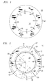
- Fig. 1 is a carrier fixture 110 used in a polishing system including a polisher (not shown) that is used during the manufacture of integrated circuits.
- the polisher is for example, an Auriga Planarization System, Auriga-C Planarization System, or a CMP 5, each available from Speedfam of 7406 West Detroit, Chandler, Arizona 85228.
- the polisher is used to polish a substrate 200, shown in Fig. 2, using, for example, chemical mechanical polishing.
- the substrate 200 is placed in the carrier fixture 110 and polished by applying a slurry and rotating the substrate disposed in the carrier fixture 110.
- the substrate 200 may be formed from materials such as silicon, germanium, gallium arsenide or other materials known to those skilled in the art.
- the carrier fixture 110 may be formed from materials such as acetal (known as DelrinTM), ceramics, and polyphenyane sulfide.
- the carrier fixture 110 has openings 115 that receive clips, screws or fasteners (not shown) to attach the carrier fixture 110 to the polisher.
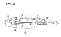
- the bottom 112 of carrier fixture 110 includes a ring member 120 that does not have the above described slurry channels for providing slurry to the substrate 200. It has been found that slurry channels are not necessary for channeling a slurry to the substrate 200 during polishing. A sufficient amount of slurry passes under the inner support 130 to the substrate 200 during polishing.
- One or more outer supports 125 are formed on the bottom 112 at the outer area or the periphery of the ring member 120.
- the outer supports 125 stabilize the ring member 120 during the polishing process.
- the outer supports 125 are spaced along the outer area so that the slurry may be channeled to the area 127 around an inner support 130.
- Each outer support 125 extends along an are of ⁇ which is, for example, 30°.
- Each outer support 125 is separated by an area extending along an arc of ⁇ which is, for example, 30°.
- the thickness X1 of the outer supports 125 is, for example, .25 inches (6.35 mm).
- the outer supports 125 and the inner support 130 do not form transport channels as in the prior art.
- the diameter X4 of the ring member 120 is, for example, 8.625 inches (219.08 mm).
- the diameter X3 of the opening 140 is, for example, 5.975 inches (151.77 mm).
- the inner support 130 is on an inner area or inner periphery of the ring member 120.
- the inner support 130 forms a ring around opening 140.
- the thickness X2 of the inner support 130 can be decreased to increase its flexibility. Increased flexibility is desirable to avoid damage to the substrate 200 when the substrate 200 contacts the inner support 130 during polishing.
- the thickness X2 is, for example, .25 inches (6.35 mm).
- the inner support 130 and the outer supports 125 project above the surface of the ring member 120 substantially the same distance Z2.
- the distance Z2 is, for example, .25 inches (6.35 mm).
- the height Z1 of the ring member 120 is, for example, .45 inches (11.42 mm).
- the substrate 200 is disposed in the carrier fixture 110 in opening 140 for the removal of material formed on the substrate 200 using, for example, chemical mechanical polishing (CMP). Approximately twelve to seventeen percent of the substrate 200 projects beyond the bottom 150 of the inner support 130 during polishing.
- the material formed on the substrate 200 is, for example, a conductive material, an oxide, silicon, or any other material which may be formed on the substrate 200.
- a slurry used for polishing a conductive material, which is typically tungsten, comprises an abrasive component and an oxidizer.
- aluminum oxide and ferric nitrate are used as the abrasive and the oxidizer, respectfully, in the slurry.
- other slurries may be used to polish other materials such as silicon and oxide.
- the conductive material is removed by a combination of physical, i.e. mechanical abrasion, and chemical, i.e., etching, processes.
- the slurry and the polisher's pad (not shown) are pressed onto the conductive material, typically at pressures of approximately 6 to 8 psi, the oxidizing component of the slurry oxidizes the conductive material to form a thin layer of metal oxide.
- This metal oxide is then readily removed with the slurry's abrasive component as the substrate 200 is rotated with respect to the pad. This process is repeated until the material is removed from the substrate 200.
- the carrier fixture 110 When the carrier fixture 110 was used in the polisher to polish tungsten formed on substrates 200, no substrate breakage was observed for 725 substrates each chemical mechanical polished for 210 seconds. In comparison, the prior art carrier fixture 510 caused substrate breakage after polishing 500 wafers for only 40 seconds each. In other words, the carrier fixture was used to successfully polish 42% more wafers for an increased duration of 425% as compared to the prior art carrier fixture.
Landscapes
- Engineering & Computer Science (AREA)
- Mechanical Engineering (AREA)
- Mechanical Treatment Of Semiconductor (AREA)
- Finish Polishing, Edge Sharpening, And Grinding By Specific Grinding Devices (AREA)
Applications Claiming Priority (4)
| Application Number | Priority Date | Filing Date | Title |
|---|---|---|---|
| US982109 | 1997-12-01 | ||
| US980943 | 1997-12-01 | ||
| US08/980,943 US5951382A (en) | 1997-12-01 | 1997-12-01 | Chemical mechanical polishing carrier fixture and system |
| US08/982,109 US5967885A (en) | 1997-12-01 | 1997-12-01 | Method of manufacturing an integrated circuit using chemical mechanical polishing |
Publications (3)
| Publication Number | Publication Date |
|---|---|
| EP0923122A2 true EP0923122A2 (de) | 1999-06-16 |
| EP0923122A3 EP0923122A3 (de) | 1999-12-29 |
| EP0923122B1 EP0923122B1 (de) | 2011-09-07 |
Family
ID=27130610
Family Applications (1)
| Application Number | Title | Priority Date | Filing Date |
|---|---|---|---|
| EP98309597A Expired - Lifetime EP0923122B1 (de) | 1997-12-01 | 1998-11-24 | Chemisch-mechanisches Polierverfahren zur Herstellung eines integrierten Schaltkreises und zugehörige Haltevorrichtung |
Country Status (3)
| Country | Link |
|---|---|
| EP (1) | EP0923122B1 (de) |
| JP (1) | JPH11239965A (de) |
| KR (1) | KR100495717B1 (de) |
Families Citing this family (2)
| Publication number | Priority date | Publication date | Assignee | Title |
|---|---|---|---|---|
| US6224472B1 (en) * | 1999-06-24 | 2001-05-01 | Samsung Austin Semiconductor, L.P. | Retaining ring for chemical mechanical polishing |
| EP1177859B1 (de) * | 2000-07-31 | 2009-04-15 | Ebara Corporation | Substrathalter und Poliervorrichtung |
Family Cites Families (2)
| Publication number | Priority date | Publication date | Assignee | Title |
|---|---|---|---|---|
| JPS63283859A (ja) * | 1987-05-13 | 1988-11-21 | Hitachi Ltd | ウェハ研磨用治具 |
| US5695392A (en) * | 1995-08-09 | 1997-12-09 | Speedfam Corporation | Polishing device with improved handling of fluid polishing media |
-
1998
- 1998-11-24 EP EP98309597A patent/EP0923122B1/de not_active Expired - Lifetime
- 1998-11-24 KR KR10-1998-0050349A patent/KR100495717B1/ko not_active Expired - Lifetime
- 1998-12-01 JP JP34087098A patent/JPH11239965A/ja active Pending
Also Published As
| Publication number | Publication date |
|---|---|
| KR100495717B1 (ko) | 2005-09-30 |
| EP0923122A3 (de) | 1999-12-29 |
| EP0923122B1 (de) | 2011-09-07 |
| KR19990062593A (ko) | 1999-07-26 |
| JPH11239965A (ja) | 1999-09-07 |
Similar Documents
| Publication | Publication Date | Title |
|---|---|---|
| US5679065A (en) | Wafer carrier having carrier ring adapted for uniform chemical-mechanical planarization of semiconductor wafers | |
| JP2943981B2 (ja) | 半導体ウェーハ用研磨パッドおよび研磨方法 | |
| US6068548A (en) | Mechanically stabilized retaining ring for chemical mechanical polishing | |
| US5842910A (en) | Off-center grooved polish pad for CMP | |
| US6180020B1 (en) | Polishing method and apparatus | |
| US7749908B2 (en) | Edge removal of silicon-on-insulator transfer wafer | |
| US5727990A (en) | Method for mirror-polishing chamfered portion of wafer and mirror-polishing apparatus | |
| EP0607940B1 (de) | Verfahren zum Schützen der Oberfläche eines halbleitenden Substrats während des Schleifens | |
| US6284658B1 (en) | Manufacturing process for semiconductor wafer | |
| WO2007032517A1 (en) | Polishing platen and polishing apparatus | |
| US5967885A (en) | Method of manufacturing an integrated circuit using chemical mechanical polishing | |
| US6406357B1 (en) | Grinding method, semiconductor device and method of manufacturing semiconductor device | |
| US6495464B1 (en) | Method and apparatus for fixed abrasive substrate preparation and use in a cluster CMP tool | |
| US5951382A (en) | Chemical mechanical polishing carrier fixture and system | |
| EP0923122B1 (de) | Chemisch-mechanisches Polierverfahren zur Herstellung eines integrierten Schaltkreises und zugehörige Haltevorrichtung | |
| JP2916028B2 (ja) | ワークエッジの鏡面研磨方法及び装置 | |
| JP4754870B2 (ja) | 研磨装置 | |
| US7008301B1 (en) | Polishing uniformity via pad conditioning | |
| KR980012155A (ko) | 패드 컨디셔너 | |
| US20070049184A1 (en) | Retaining ring structure for enhanced removal rate during fixed abrasive chemical mechanical polishing | |
| JPH10109263A (ja) | 化学的機械研磨方法及び化学的機械研磨装置 | |
| EP1297927A2 (de) | Poliervorrichtung | |
| EP1308243B1 (de) | Polierverfahren | |
| JP2004106134A (ja) | 加工用基板固定装置およびその製造方法 | |
| JP3020905B2 (ja) | シリコン半導体ウエハ |
Legal Events
| Date | Code | Title | Description |
|---|---|---|---|
| PUAI | Public reference made under article 153(3) epc to a published international application that has entered the european phase |
Free format text: ORIGINAL CODE: 0009012 |
|
| AK | Designated contracting states |
Kind code of ref document: A2 Designated state(s): DE |
|
| AX | Request for extension of the european patent |
Free format text: AL;LT;LV;MK;RO;SI |
|
| PUAL | Search report despatched |
Free format text: ORIGINAL CODE: 0009013 |
|
| AK | Designated contracting states |
Kind code of ref document: A3 Designated state(s): AT BE CH CY DE DK ES FI FR GB GR IE IT LI LU MC NL PT SE |
|
| AX | Request for extension of the european patent |
Free format text: AL;LT;LV;MK;RO;SI |
|
| RIC1 | Information provided on ipc code assigned before grant |
Free format text: 6H 01L 21/68 A, 6B 24B 37/04 B |
|
| 17P | Request for examination filed |
Effective date: 20000615 |
|
| AKX | Designation fees paid |
Free format text: DE |
|
| 17Q | First examination report despatched |
Effective date: 20060310 |
|
| RAP3 | Party data changed (applicant data changed or rights of an application transferred) |
Owner name: LUCENT TECHNOLOGIES INC. |
|
| GRAP | Despatch of communication of intention to grant a patent |
Free format text: ORIGINAL CODE: EPIDOSNIGR1 |
|
| RTI1 | Title (correction) |
Free format text: METHOD OF MANUFACTURING AN INTEGRATED CIRCUIT USING CHEMICAL MECHANICAL POLISHING AND FIXTURE FOR CHEMICAL MECHANICAL POLISHING |
|
| GRAS | Grant fee paid |
Free format text: ORIGINAL CODE: EPIDOSNIGR3 |
|
| GRAA | (expected) grant |
Free format text: ORIGINAL CODE: 0009210 |
|
| AK | Designated contracting states |
Kind code of ref document: B1 Designated state(s): DE |
|
| REG | Reference to a national code |
Ref country code: DE Ref legal event code: R096 Ref document number: 69842401 Country of ref document: DE Effective date: 20111103 |
|
| PLBE | No opposition filed within time limit |
Free format text: ORIGINAL CODE: 0009261 |
|
| STAA | Information on the status of an ep patent application or granted ep patent |
Free format text: STATUS: NO OPPOSITION FILED WITHIN TIME LIMIT |
|
| 26N | No opposition filed |
Effective date: 20120611 |
|
| REG | Reference to a national code |
Ref country code: DE Ref legal event code: R097 Ref document number: 69842401 Country of ref document: DE Effective date: 20120611 |
|
| PGFP | Annual fee paid to national office [announced via postgrant information from national office to epo] |
Ref country code: DE Payment date: 20171019 Year of fee payment: 20 |
|
| REG | Reference to a national code |
Ref country code: DE Ref legal event code: R082 Ref document number: 69842401 Country of ref document: DE Representative=s name: DILG HAEUSLER SCHINDELMANN PATENTANWALTSGESELL, DE Ref country code: DE Ref legal event code: R081 Ref document number: 69842401 Country of ref document: DE Owner name: AVAGO TECHNOLOGIES GENERAL IP (SINGAPORE) PTE., SG Free format text: FORMER OWNER: LUCENT TECHNOLOGIES, INC., MURRAY HILL, N.J., US |
|
| REG | Reference to a national code |
Ref country code: DE Ref legal event code: R071 Ref document number: 69842401 Country of ref document: DE |