EP0923189A2 - Spannungskonverter - Google Patents
Spannungskonverter Download PDFInfo
- Publication number
- EP0923189A2 EP0923189A2 EP98204109A EP98204109A EP0923189A2 EP 0923189 A2 EP0923189 A2 EP 0923189A2 EP 98204109 A EP98204109 A EP 98204109A EP 98204109 A EP98204109 A EP 98204109A EP 0923189 A2 EP0923189 A2 EP 0923189A2
- Authority
- EP
- European Patent Office
- Prior art keywords
- voltage
- output
- transformer
- circuit
- secondary winding
- Prior art date
- Legal status (The legal status is an assumption and is not a legal conclusion. Google has not performed a legal analysis and makes no representation as to the accuracy of the status listed.)
- Withdrawn
Links
Images


Classifications
-
- H—ELECTRICITY
- H02—GENERATION; CONVERSION OR DISTRIBUTION OF ELECTRIC POWER
- H02M—APPARATUS FOR CONVERSION BETWEEN AC AND AC, BETWEEN AC AND DC, OR BETWEEN DC AND DC, AND FOR USE WITH MAINS OR SIMILAR POWER SUPPLY SYSTEMS; CONVERSION OF DC OR AC INPUT POWER INTO SURGE OUTPUT POWER; CONTROL OR REGULATION THEREOF
- H02M3/00—Conversion of DC power input into DC power output
- H02M3/22—Conversion of DC power input into DC power output with intermediate conversion into AC
- H02M3/24—Conversion of DC power input into DC power output with intermediate conversion into AC by static converters
- H02M3/28—Conversion of DC power input into DC power output with intermediate conversion into AC by static converters using discharge tubes with control electrode or semiconductor devices with control electrode to produce the intermediate AC
-
- H—ELECTRICITY
- H02—GENERATION; CONVERSION OR DISTRIBUTION OF ELECTRIC POWER
- H02M—APPARATUS FOR CONVERSION BETWEEN AC AND AC, BETWEEN AC AND DC, OR BETWEEN DC AND DC, AND FOR USE WITH MAINS OR SIMILAR POWER SUPPLY SYSTEMS; CONVERSION OF DC OR AC INPUT POWER INTO SURGE OUTPUT POWER; CONTROL OR REGULATION THEREOF
- H02M1/00—Details of apparatus for conversion
- H02M1/0083—Converters characterised by their input or output configuration
- H02M1/009—Converters characterised by their input or output configuration having two or more independently controlled outputs
Definitions
- the first-mentioned output is on High voltage output, the one opposite to the input side AC voltage or compared to that resulting from the rectifier arrangement obtained direct voltage on the electronic switch significant provides higher DC output voltage, and are also the other DC supply voltages in contrast, is designed as a low-voltage output because of the higher gear ratio then chosen between the Primary winding and the secondary winding of the transformer on the output side Capacitance, which is a parallel capacitance of the so-called high voltage output of the Voltage converter forms the operating behavior of this voltage converter determine decisively, since they are on the primary side of the transformer with this high gear ratio transformed to a relatively high value becomes.
- a mutual influence that is called “cross-regulation” is called and which is noticeable in that the Output voltages, i.e. the high voltage and the other DC supply voltages, are not solely dependent on their mutual relationship Number of turns of the secondary windings or parts of the secondary winding, but also of their respective loads. That means that despite regulation a of the DC voltages to a fixed value for the other DC voltages Fluctuations occur that depend on the loads on the outputs.
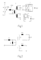
- Fig. 1 shows a more detailed explanation of the problem of "cross regulation" Voltage converter for converting an input voltage UB into a high one DC voltage and another supply voltage.
- This voltage converter contains two switches 4, 5 arranged in series, which act as chopper switches between the input voltage UB and ground 6 alternately periodically conductive and locked.
- Parallel to the second of these switches with the Reference numeral 5 is the series connection of a resonance capacitance CRES, one Resonance inductance LRES and the primary winding of a transformer T connected, which is located between nodes A and B.
- the Resonance capacitance CRES and the resonance inductance LRES are elements of one Input resonance circuit of the voltage converter, in which also the primary winding of the transformer T is included.
- the transformer T has two secondary windings, a first of which Nodes H and V and a second at nodes J and K is led. Of the Transformer T is at nodes H and V to deliver one AC of high amplitude and at nodes J and K for delivery dimensioned another AC voltage.
- the first secondary winding between nodes H and V is therefore also called a high voltage winding designated.
- the further AC voltage on the second secondary winding between the nodes J and K has a much lower amplitude; in the Contrary to the AC voltage of high amplitude (high voltage) on the first Secondary winding is also referred to below as low voltage.
- the first output circuit which is the first secondary winding between the Including nodes H and V is to provide the high DC voltage designed
- the second output circuit which is the second secondary winding between including nodes J and K is to supply the others Supply voltage designed.
- the first output circuit comprises that in FIG. 1 illustrated voltage converter a voltage multiplier 7, the output is connected to a load capacity CL2, at which the high DC voltage sets. There is a between the nodes H and V.
- Parallel capacitance CP inserted depending on the design of the voltage converter by the parasitic winding capacitance of the first secondary winding Transformer T in the first output circuit or by a separate component be educated.
- the output circuit of the second secondary winding 1 comprises a bridge rectifier, the four Contains diodes D1, D2, D3 and D4. This bridge rectifier is on the output side connected to a load capacity CL3, on which the other is in operation Sets supply voltage.
- FIG. 2 shows an equivalent circuit diagram for the transformer T.
- This includes between nodes A and B as an equivalent circuit for the primary winding a series connection of a primary leakage inductance LS1 with a Parallel connection of a main inductance LH of the transformer T and one Primary winding 1 of an ideal transformer.
- This includes on the secondary side 2 for the first secondary winding, the winding 2 of the ideal transformer in series with a secondary leakage inductance LS2 between the nodes H and V and accordingly a series connection of one another secondary winding 3 of the ideal transformer with its associated secondary-side leakage inductance LS3 between the nodes J and K.
- Aus The values can be found in the technical data of the transformer T to be used determine clearly for the leakage inductances.
- the equivalent circuit diagram of the Fig. 2 is also the parallel capacitance CP to the first secondary winding 2 between the nodes H and V are drawn.
- FIG. 3 Another explanation is given in FIG. 3 to explain the problem of "cross regulation" Simplification of the equivalent circuit diagram of the transformer T together with the most important other elements of the voltage converter shown in Fig. 1.
- the Simplification of the equivalent circuit diagram is that the secondary side Elements of the transformer T with the associated gear ratios the primary side of the transformer T are converted so that a simplified, galvanically coupled equivalent circuit diagram results.
- LS22 is the secondary leakage inductance LS2, transformed on the primary side, designated.
- LS33 denotes the leakage inductance LS3 on the secondary side, transformed to the primary side of the transformer T.
- CP22 the Parallel capacitance CP in its on the primary side of the transformer T transformed form.
- H22, V22, J33 and K33 designate accordingly the nodes corresponding to the nodes H, V, J and K respectively transformed circuit. 1 during operation of the voltage converter 3 between the nodes A and B for the equivalent circuit of FIG Voltage uAB, the voltage uH22V22 between nodes H22 and V22 and the voltage uJ33K33 between the nodes J33 and K33.
- the Primary circuit of the voltage converter i.e. the input resonance circuit with the The primary winding of the transformer T has been further simplified in FIG. 3. So is the leakage inductance LS1 with the resonance inductance LRES to one resulting resonance inductance LS1RES have been summarized. Since the LH's main inductance can usually be regarded as high impedance, it is in Fig. 3 not shown. A current i flows in the input resonance circuit during operation.
- Fig. 4 shows the operation of the voltage converter according to Fig. 1 in 3 and the current i im Input resonant circuit.
- the display begins at a time ts at which the transformed parallel capacitance CP22 is completely discharged.
- The is accordingly Voltage uH22V22 at time ts is zero.
- the voltage is correct in a first approximation uAB corresponds to the voltage uH22V22 in this operating state. Both rise starting at time ts starting from zero.
- the described operating state changes at time t0, at which the Parallel capacitance CP22 is charged so far that the voltage uAB and thus the Voltage uJ33K33 reach a value U which is the further supply DC voltage to which the load capacity CL3 is charged during operation, transforms to the primary side of the transformer T.
- the bridge rectifier D1, D2, D3, D4 conductive, and the voltage uJ33K33 remains at the value U.
- the equivalent circuit diagram for this operating case is shown in FIG. 5, in the rest of the elements already explained with matching reference numerals are provided.
- FIG. 6 A section of FIG. 6 explains the rise in voltage uH22V22 shown from the equivalent circuit of Fig. 3, wherein those already described Elements are again provided with matching reference numerals.
- the one in Fig. 6 Excerpt shown includes the transformed secondary leakage inductance LS22 and the transformed parallel capacitance CP22. It turns out that this E elements in the described operating situation a series connection from one Form inductance and a capacitance to which at time t0 Voltage jump corresponding to the voltage U is applied.
- the tension that forms on the parallel capacitance CP22 transformed on the primary side has a sinusoidal curve, the amplitude of which is proportional to the value of the Current i in the input resonance circuit at time t0 and inversely proportional to the value of the transformed parallel capacitance is CP22. Besides, this is Amplitude inversely proportional to the period of the sinusoidal Voltage curve, which in turn is derived from the reciprocal of the square root of the Product of the transformed parallel capacitance CP22 and the transformed Scattering inductance LS22 determined.
- the voltage surge i.e. the amplitude of the sinusoidal curve of the voltage uH22V22 after the time t0, as in Fig.
- the invention now has the task of a voltage converter of the beginning type described with several outputs in such a way that a improved synchronization of the output voltages, i.e. a decreased "Cross regulation", as can be achieved in a conventional manner.
- this object is achieved in a voltage converter Generic type solved by (each) an additional capacity parallel to Secondary winding of the transformer in the (s) Rectifier arrangement (s) having the remaining output circuit (s), the additional capacity (s) is (are) such that you can focus on the Primary side of the transformer transformed value (or transformed values in Sum) essentially with the value of a transformed on the primary side Parallel capacitance of the secondary winding of the transformer from the first Output circuit matches.
- the output circuits can either to different taps of a secondary winding or to individual ones Output circuits or groups of output circuits are electrically isolated Secondary windings are connected.
- the voltage converter can pass through the parallel capacitance from the first output circuit a parasitic winding capacitance, through a separate capacitive component or be a combination of both.
- the current i in the input resonance circuit of the parallel capacity exclusively in the first output circuit to at least one distributed further output circle.
- This causes the current to leakage inductance LS2 or LS22 reduced in the first output circuit at time t0.
- This Decrease also outweighs an increase in current i due to the increase the capacitive load on the secondary side of the transformer T.
- the voltage converter can be reduced the "cross-regulation" of about 30%. This is with very little additional circuitry possible.
- This inventive design of the voltage converter makes it possible to Current through the secondary leakage inductance of the first secondary winding (High voltage winding) of the transformer at the beginning of the voltage surge - see. 4 - to force zero at time t0 in FIG. Because the voltage surge is proportional to this current, it can also be made zero. In order to the "cross regulation" can at least be largely eliminated. To do this reach is at least one of the other output circles of the Voltage converter each assigned an auxiliary circuit, which with its additional Secondary winding of the transformer and its additional capacitor vibrating circuit structure forms.
- the additional rectifier arrangement causes only in the auxiliary circuit a current flows in the time surrounding the beginning of the voltage surge.
- the series connection included in the auxiliary circuit is additional Secondary winding, additional capacitor and additional Rectifier arrangement further parallel to a branch of the rectifier arrangement the relevant output circuit and the load connected to it.
- a tuning resistor can be arranged with which the amplitude of the Current in the auxiliary circuit can be adjusted to a value by which one complete cross-regulation is achieved.
- the circuitry can thus be increased somewhat at least largely rule out cross-regulation.
- this voltage converter is the additional rectifier arrangement or are the additional ones Rectifier arrangements designed as bridge rectifiers.
- Such a Bridge rectifier is preferably equivalent to the rectifier arrangement of the associated output circuit connected to its load.
- the rectifier arrangement (s) of the output circuit are also designed as bridge rectifiers.
- a part of Elements of the bridge rectifier of an output circuit is also part of the additional rectifier arrangement of the same output circuit.
- Voltage converters of the inventive type are advantageous in electrical devices of all kinds can be used in which several loads are fed from one energy source with one of the loads having a higher load than the other loads electrical voltage is to be supplied.
- the invention Voltage converter suitable for use in mains-powered devices such as Monitors, television receivers or the like.
- Fig. 7 shows a circuit arrangement for a voltage converter, the largely corresponds to the circuit arrangement according to FIG. 1. In this respect, the Description of Fig. 1 referenced.
- Fig. 7 shows an additional capacitance CL, which with the second secondary winding of the transformer T connected output circuit between the nodes J and K is arranged parallel to the secondary winding.
- This additional capacity CL is dimensioned so that you with the gear ratio between the second Secondary winding (low voltage winding) and the primary winding of the Transformer T on the primary side converted capacitance value just as large is like the one with the gear ratio between the first secondary winding (High voltage winding) and the primary winding of the transformer T converted capacity value of the parallel capacity CP in the first output circuit between the nodes H and V.
- the current i in the input resonance circuit then distributed at least almost evenly between the two output circles. The excess voltage is thus reduced by about 30%.
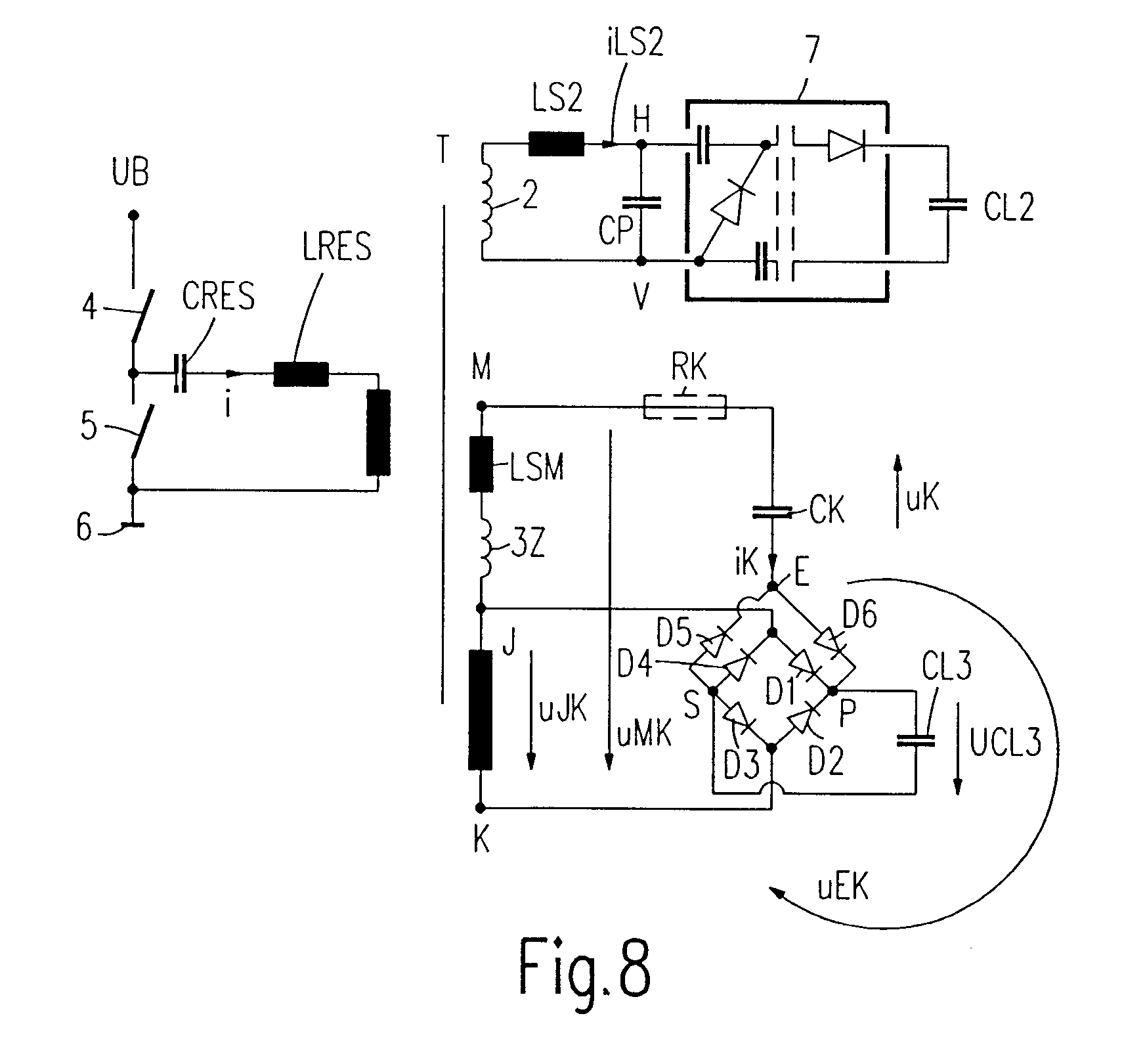
- FIG. 8 shows a second exemplary embodiment of an inventive one Voltage converter shown, which is also related to the voltage converter 1 based on.
- This auxiliary circuit includes an additional secondary winding, the also applied to the core of the transformer T and on one side with the Junction J is connected.
- the second connection of this additional Secondary winding forms another node M.
- the further node M is via an additional capacitor CK and, if appropriate, one in Row-arranged tuning resistor RK connected to a node E, which forms a connection point of an additional rectifier arrangement.
- This additional rectifier arrangement includes the diodes D2 and D3 Rectifier arrangement of the output circuit and two further diodes D5 and D6 and is - like the rectifier arrangement of the output circuit - as Bridge rectifier designed.
- the nodes E and K form AC input terminals of the additional rectifier assembly.
- the Nodes J and K form AC input terminals of the Rectifier arrangement D1, D2, D3, D4 of the output circuit, and the load capacity CL3 of this output circuit, on which the further DC supply voltage U can be tapped is connected to nodes P and S, which the DC output terminals of both the additional Rectifier arrangement D2, D3, D5, D6 as well as the rectifier arrangement D1, Form D2, D3, D4 of the output circuit.
- the diode D1 is between the Nodes J and P, D2 between P and K, D3 between K and S, D4 between S and J, D5 between S and E and D6 between E and P.
- D2 and D3 are elements of both the rectifier arrangement of the output circuit and also the additional rectifier arrangement.
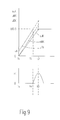
- Fig. 9 To illustrate the operation of the embodiment of FIG. 8 is on Fig. 9 referenced.
- DC voltage uK which is approximately equal to the peak value of the voltage across the additional secondary winding between the nodes M and J and a Has polarity
- the current value of the voltage uMK between the Junctions M and K enlarged.
- the polarity of the voltage uK at the additional Capacitor CK is due to the current caused by this additional Capacitor CK in the previous half period of current i im Input resonance circuit or the voltage uAB has flowed.
- the voltage uMK In the upper part of the 9 is the profile of the voltage uMK for the beginning of a half-wave plotted in which the potential at node M compared to the potential at Node K rises continuously.
- uJK the tension between the Designated nodes J and K, i.e. the on the secondary winding of the Output circuit forming voltage.
- the voltage uMK the ratio of the number of turns between the nodes M and K on the one hand and the nodes J and K on the other hand proportional enlarged.
- the voltage uEK between the nodes E and K, resulting from the sum of the voltages uK and uMK is compared to that The voltage uMK is shifted by the DC voltage uK.
- the voltage uEK increases with the voltage uMK until it is ta at a time the value of the further supply DC voltage UCL3 at the load capacitance CL3 reached.
- the voltage UCL3 is transformed to the primary side of the Transformer T with the associated gear ratio to that already described voltage U.
- Neglecting the diode flux voltages of the Diodes D3 and D6 set a current iK through the additional one at time ta Capacitor CK and thus through the auxiliary circuit, which forms an oscillation, whose period duration by the leakage inductance LSM the additional Secondary winding and the additional capacitor CK is determined.
- the amplitude of this vibration is determined by the value that the Voltage uEK would reach if one followed its course before the time ta extra polished at time t0.
- the time t0 is identical to that in Fig. 4 shown the beginning of the excessive voltage.
- the current iK through the additional capacitor CK is shown in the lower part of FIG. 9 and forms a waveform with a semisine-like course, the maximum of which is a quarter of the period of the mentioned vibration, calculated from Time ta on occurs.
- the semisine-like wave of the described Vibration extends over a time interval that the time t0, i.e. the Includes beginning of voltage surge.
- the time t0 caused by the current i in the input resonance circuit, except for the current in the first secondary winding (high voltage winding) of the transformer T, which in Fig. 8 is entered as iLS2, also the current iK in the additional Secondary winding and the additional capacitor CK.
- time t0 thus competition between the current paths for the currents iLS2 and iK.
- Fig. 10 shows a further embodiment of the invention, which by a Modification of the circuit arrangement according to FIG. 8 has arisen.
- the diode D4 has been omitted, the diode D1 forms without the Auxiliary circuit a one-way rectifier for the from the nodes J and K supplied AC voltage to form the DC voltage UCL3 over the Load capacity CL3.
- the auxiliary group for this arrangement with the additional Secondary winding between nodes M and J, the additional one Capacitor CK and the additional bridge rectifier from diodes D2, D3, D5 and D6 and possibly with the tuning resistor RK is with the auxiliary circuit shown in Fig. 8 identical.
- the exemplary embodiments according to FIGS. 8 and 10 can be expanded by further Secondary windings and the output circuit connected to them are expanded, these output circuits can optionally be equipped with additional auxiliary circuits can.
- the invention provides a significant improvement in synchronism of the output voltages of the output circuits of the voltage converter.
- voltage converters become a broad field of application for Devices opened up where high demands are placed on synchronism be used, for example, for monitors and television receivers.
Landscapes
- Engineering & Computer Science (AREA)
- Power Engineering (AREA)
- Dc-Dc Converters (AREA)
- Electrotherapy Devices (AREA)
- Rectifiers (AREA)
Abstract
- einen Eingangsresonanzkreis, in den eine Primärwicklung eines Transformators einbezogen ist und dem die Eingangsspannung in periodisch wiederkehrenden Zeitintervallen zuführbar ist,
- wenigstens zwei Ausgangskreise, in die je eine Sekundärwicklung oder ein Teil
einer Sekundärwicklung des Transformators einbezogen ist und denen je eine
der Ausgangsspannungen entnehmbar ist, wobei
- eine von einem ersten der Ausgangskreise gelieferte erste der Ausgangsspannungen eine Hochspannung und die übrige(n) Ausgangsspannung(en) (eine) demgegenüber niedrige Spannung(en) bildet (bzw. bilden),
- wenigstens (einer) der die übrige(n) Ausgangsspannung(en) liefernde(n) übrige(n) Ausgangskreis(e) eine Gleichrichteranordnung zum Liefern einer Gleichspannung als Ausgangsspannung aufweist.
- jeder Hilfskreis eine zusätzliche Sekundärwicklung des Transformators umfaßt, die mit einem zusätzlichen Kondensator und einer zusätzlichen Gleichrichteranordnung in einer Reihenschaltung angeordnet ist und
- diese Reihenschaltung parallel zu einem Zweig der Gleichrichteranordnung des betreffenden Ausgangskreises sowie einer mit diesem verbundenen Last angeordnet ist.
Description
- einen Eingangsresonanzkreis, in den eine Primärwicklung eines Transformators einbezogen ist und dem die Eingangsspannung in periodisch wiederkehrenden Zeitintervallen zuführbar ist,
- wenigstens zwei Ausgangskreise, in die je eine Sekundärwicklung oder ein Teil
einer Sekundärwicklung des Transformators einbezogen ist und denen je eine
der Ausgangsspannungen entnehmbar ist, wobei
- eine von einem ersten der Ausgangskreise gelieferte erste der Ausgangsspannungen eine Hochspannung und die übrige(n) Ausgangsspannung(en) (eine) demgegenüber niedrige Spannung(en) bildet (bzw. bilden),
- wenigstens (einer) der die übrige(n) Ausgangsspannung(en) liefernde(n) übrige(n) Ausgangskreis(e) eine Gleichrichteranordnung zum Liefern einer Gleichspannung als Ausgangsspannung aufweist.
- jeder Hilfskreis eine zusätzliche Sekundärwicklung des Transformators umfaßt, die mit einem zusätzlichen Kondensator und einer zusätzlichen Gleichrichteranordnung in einer Reihenschaltung angeordnet ist und
- diese Reihenschaltung parallel zu einem Zweig der Gleichrichteranordnung des betreffenden Ausgangskreises sowie einer mit diesem verbundenen Last angeordnet ist.
Claims (5)
- Spannungskonverter zum Konvertieren einer Eingangsspannung in wenigstens zwei Ausgangsspannungen, umfassendgekennzeichnet durcheinen Eingangsresonanzkreis, in den eine Primärwicklung eines Transformators einbezogen ist und dem die Eingangsspannung in periodisch wiederkehrenden Zeitintervallen zuführbar ist,wenigstens zwei Ausgangskreise, in die je eine Sekundärwicklung oder ein Teil einer Sekundärwicklung des Transformators einbezogen ist und denen je eine der Ausgangsspannungen entnehmbar ist, wobeieine von einem ersten der Ausgangskreise gelieferte erste der Ausgangsspannungen eine Hochspannung und die übrige(n) Ausgangsspannung(en) (eine) demgegenüber niedrige Spannung(en) bildet (bzw. bilden),wenigstens (einer) der die übrige(n) Ausgangsspannung(en) liefernde(n) übrige(n) Ausgangskreis(e) eine Gleichrichteranordnung zum Liefern einer Gleichspannung als Ausgangsspannung aufweist,
(je) eine zusätzliche Kapazität parallel zur Sekundärwicklung des Transformators in dem (bzw. den) die Gleichrichteranordnung(en) aufweisenden übrigen Ausgangskreis(en), wobei die zusätzliche(n) Kapazität(en) derart bemessen ist (bzw. sind), daß ihr(e) auf die Primärseite des Transformators transformierter Wert (bzw. transformierten Werte in Summe) im wesentlichen mit dem auf die Primärseite transformierten Wert einer Parallelkapazität der Sekundärwicklung des Transformators aus dem ersten Ausgangskreis übereinstimmt. - Spannungskonverter zum Konvertieren einer Eingangsspannung in wenigstens zwei Ausgangsspannungen, umfassendgekennzeichnet durcheinen Eingangsresonanzkreis, in den eine Primärwicklung eines Transformators einbezogen ist und dem die Eingangsspannung in periodisch wiederkehrenden Zeitintervallen zuführbar ist,wenigstens zwei Ausgangskreise, in die je eine Sekundärwicklung oder ein Teil einer Sekundärwicklung des Transformators einbezogen ist und denen je eine der Ausgangsspannungen entnehmbar ist, wobeieine von einem ersten der Ausgangskreise gelieferte erste der Ausgangsspannungen eine Hochspannung und die übrige(n) Ausgangsspannung(en) (eine) demgegenüber niedrige Spannung(en) bildet (bzw. bilden),wenigstens (einer) der die übrige(n) Ausgangsspannung(en) liefernde(n) übrige(n) Ausgangskreis(e) eine Gleichrichteranordnung zum Liefern einer Gleichspannung als Ausgangsspannung aufweist,
(je) einen Hilfskreis in dem (bzw. den) die Gleichrichteranordnung(en) aufweisenden übrigen Ausgangskreis(en), wobeijeder Hilfskreis eine zusätzliche Sekundärwicklung des Transformators umfaßt, die mit einem zusätzlichen Kondensator und einer zusätzlichen Gleichrichteranordnung in einer Reihenschaltung angeordnet ist unddiese Reihenschaltung parallel zu einem Zweig der Gleichrichteranordnung des betreffenden Ausgangskreises sowie einer mit diesem verbundenen Last angeordnet ist. - Spannungskonverter nach Anspruch 2, dadurch gekennzeichnet,
daß die zusätzliche(n) Gleichrichteranordnung(en) als Brückengleichrichter ausgebildet ist (sind). - Spannungskonverter nach Anspruch 3, dadurch gekennzeichnet,
daß die Gleichrichteranordnung(en) des Ausgangskreises (bzw. der Ausgangskreise) als Brückengleichrichter ausgebildet ist (bzw. sind) und ein Teil der Elemente des Brückengleichrichters eines Ausgangskreises zugleich Teil der zusätzlichen Gleichrichteranordnung desselben Ausgangskreises ist. - Elektrisches Gerät, gekennzeichnet durch
einen Spannungskonverter nach einem der Ansprüche 1 bis 4.
Applications Claiming Priority (2)
| Application Number | Priority Date | Filing Date | Title |
|---|---|---|---|
| DE19754846A DE19754846A1 (de) | 1997-12-10 | 1997-12-10 | Spannungskonverter |
| DE19754846 | 1997-12-10 |
Publications (2)
| Publication Number | Publication Date |
|---|---|
| EP0923189A2 true EP0923189A2 (de) | 1999-06-16 |
| EP0923189A3 EP0923189A3 (de) | 2000-12-20 |
Family
ID=7851423
Family Applications (1)
| Application Number | Title | Priority Date | Filing Date |
|---|---|---|---|
| EP98204109A Withdrawn EP0923189A3 (de) | 1997-12-10 | 1998-12-03 | Spannungskonverter |
Country Status (4)
| Country | Link |
|---|---|
| US (1) | US6072709A (de) |
| EP (1) | EP0923189A3 (de) |
| JP (1) | JPH11266585A (de) |
| DE (1) | DE19754846A1 (de) |
Families Citing this family (9)
| Publication number | Priority date | Publication date | Assignee | Title |
|---|---|---|---|---|
| DE10122534A1 (de) * | 2001-05-09 | 2002-11-21 | Philips Corp Intellectual Pty | Resonanter Konverter |
| JP2007174793A (ja) * | 2005-12-21 | 2007-07-05 | Sanken Electric Co Ltd | 多出力スイッチング電源装置 |
| JP4335871B2 (ja) * | 2005-12-27 | 2009-09-30 | 新電元工業株式会社 | スイッチング電源装置及びサージ吸収回路 |
| US20080068132A1 (en) * | 2006-05-16 | 2008-03-20 | Georges Kayanakis | Contactless radiofrequency device featuring several antennas and related antenna selection circuit |
| AU2011250957B2 (en) * | 2010-05-10 | 2014-10-23 | Enphase Energy, Inc. | Lossless commutation during operation of a power converter |
| US10188446B2 (en) * | 2013-10-16 | 2019-01-29 | Covidien Lp | Resonant inverter |
| WO2015192133A2 (en) | 2014-06-13 | 2015-12-17 | University Of Maryland | An integrated dual-output grid-to-vehicle (g2v) and vehicle-to-grid (v2g) onboard charger for plug-in electric vehicles |
| KR20160004053A (ko) * | 2014-07-02 | 2016-01-12 | 주식회사 솔루엠 | 다중 출력 전원 공급 장치 및 그의 출력 회로 |
| KR102751327B1 (ko) | 2019-08-01 | 2025-01-07 | 삼성전자주식회사 | 복수의 전압 레귤레이터들을 포함하는 전자 시스템 |
Family Cites Families (5)
| Publication number | Priority date | Publication date | Assignee | Title |
|---|---|---|---|---|
| US4695934A (en) * | 1985-05-13 | 1987-09-22 | General Electric Company | Multiple output resonant power supply |
| US4628426A (en) * | 1985-10-31 | 1986-12-09 | General Electric Company | Dual output DC-DC converter with independently controllable output voltages |
| US5363287A (en) * | 1994-03-01 | 1994-11-08 | Philips Electronics North America Corporation | Low noise multi-output and multi-resonant forward converter for television power supplies |
| US5737203A (en) * | 1994-10-03 | 1998-04-07 | Delco Electronics Corp. | Controlled-K resonating transformer |
| DE19529941A1 (de) * | 1995-08-16 | 1997-02-20 | Philips Patentverwaltung | Spannungskonverter |
-
1997
- 1997-12-10 DE DE19754846A patent/DE19754846A1/de not_active Withdrawn
-
1998
- 1998-12-03 EP EP98204109A patent/EP0923189A3/de not_active Withdrawn
- 1998-12-04 US US09/205,974 patent/US6072709A/en not_active Expired - Fee Related
- 1998-12-09 JP JP10350275A patent/JPH11266585A/ja active Pending
Also Published As
| Publication number | Publication date |
|---|---|
| EP0923189A3 (de) | 2000-12-20 |
| DE19754846A1 (de) | 1999-06-17 |
| US6072709A (en) | 2000-06-06 |
| JPH11266585A (ja) | 1999-09-28 |
Similar Documents
| Publication | Publication Date | Title |
|---|---|---|
| DE69807251T2 (de) | Aufwärtswandler | |
| DE19545154C2 (de) | Stromversorgungseinrichtung | |
| DE3325612C2 (de) | ||
| DE19710319B4 (de) | Schaltung zum Sperren einer Halbleiterschaltvorrichtung bei Überstrom | |
| DE4426258B4 (de) | Umrichter | |
| DE102011118581A1 (de) | Kontaktloses Energieübertragungssystem und Steuerverfahren dafür | |
| DE10122534A1 (de) | Resonanter Konverter | |
| EP0758815B1 (de) | Spannungskonverter | |
| DE19546287B4 (de) | Leistungsschaltkreis | |
| EP0301436B1 (de) | Gleichspannungswandler | |
| EP1152519B1 (de) | DC-DC-Konverter | |
| DE60101234T2 (de) | Schaltnetzteilgerät | |
| DE2644553C3 (de) | Schaltungsanordnung zur Regulierung der von einem Wechselstromnetz an einen Verbraucher abgegebenen elektrischen Leistung | |
| EP0923189A2 (de) | Spannungskonverter | |
| DE3040556C2 (de) | ||
| DD217955A5 (de) | Speisespannungsschaltung | |
| DE60128040T2 (de) | Stromversorgung und diese stromversorgung benutzende elektronische vorrichtung | |
| DE4414677A1 (de) | Primärgetakteter Spannungswandler, insbesondere für hohe Eingangsgleichspannungen | |
| DE4001325B4 (de) | Gleichspannungssperrwandler | |
| EP3783630B1 (de) | Vorrichtung zum unterdrücken eines gleichstromanteils beim betrieb eines an ein hochspannungsnetz angeschlossenen elektrischen geräts | |
| EP0475296B1 (de) | Getaktete Stromversorgunseinrichtung mit einem Fluss- und einem Sperrwandlerausgang | |
| EP1205021A1 (de) | Verfahren zur regelung eines schaltnetzteiles und schaltnetzteil | |
| DE4124616A1 (de) | Schaltungsanordnung zum speisen wenigstens einer last | |
| DE2921400C2 (de) | ||
| DE2443892B1 (de) | Schaltungsanordnung zur Herabsetzung der auftretenden Verlustleistung beim Abschalten einer wenigstens einen Halbleiterschalter und eine Induktanz enthaltenden Reihenschaltung |
Legal Events
| Date | Code | Title | Description |
|---|---|---|---|
| PUAI | Public reference made under article 153(3) epc to a published international application that has entered the european phase |
Free format text: ORIGINAL CODE: 0009012 |
|
| AK | Designated contracting states |
Kind code of ref document: A2 Designated state(s): DE FR GB |
|
| AX | Request for extension of the european patent |
Free format text: AL;LT;LV;MK;RO;SI |
|
| RAP3 | Party data changed (applicant data changed or rights of an application transferred) |
Owner name: KONINKLIJKE PHILIPS ELECTRONICS N.V. Owner name: PHILIPS CORPORATE INTELLECTUAL PROPERTY GMBH |
|
| RIC1 | Information provided on ipc code assigned before grant |
Free format text: 7H 02M 3/28 A, 7H 02M 3/335 B |
|
| PUAL | Search report despatched |
Free format text: ORIGINAL CODE: 0009013 |
|
| AK | Designated contracting states |
Kind code of ref document: A3 Designated state(s): AT BE CH CY DE DK ES FI FR GB GR IE IT LI LU MC NL PT SE |
|
| AX | Request for extension of the european patent |
Free format text: AL;LT;LV;MK;RO;SI |
|
| 17P | Request for examination filed |
Effective date: 20010620 |
|
| AKX | Designation fees paid |
Free format text: DE FR GB |
|
| RAP1 | Party data changed (applicant data changed or rights of an application transferred) |
Owner name: KONINKLIJKE PHILIPS ELECTRONICS N.V. Owner name: PHILIPS CORPORATE INTELLECTUAL PROPERTY GMBH |
|
| STAA | Information on the status of an ep patent application or granted ep patent |
Free format text: STATUS: THE APPLICATION HAS BEEN WITHDRAWN |
|
| 18W | Application withdrawn |
Withdrawal date: 20021104 |