EP0924749A2 - Vorrichtung zur magnetischen Abschirmung - Google Patents
Vorrichtung zur magnetischen Abschirmung Download PDFInfo
- Publication number
- EP0924749A2 EP0924749A2 EP98124436A EP98124436A EP0924749A2 EP 0924749 A2 EP0924749 A2 EP 0924749A2 EP 98124436 A EP98124436 A EP 98124436A EP 98124436 A EP98124436 A EP 98124436A EP 0924749 A2 EP0924749 A2 EP 0924749A2
- Authority
- EP
- European Patent Office
- Prior art keywords
- tubular member
- magnetic shield
- opening
- flange portion
- distal end
- Prior art date
- Legal status (The legal status is an assumption and is not a legal conclusion. Google has not performed a legal analysis and makes no representation as to the accuracy of the status listed.)
- Withdrawn
Links
Images


Classifications
-
- H—ELECTRICITY
- H05—ELECTRIC TECHNIQUES NOT OTHERWISE PROVIDED FOR
- H05K—PRINTED CIRCUITS; CASINGS OR CONSTRUCTIONAL DETAILS OF ELECTRIC APPARATUS; MANUFACTURE OF ASSEMBLAGES OF ELECTRICAL COMPONENTS
- H05K9/00—Screening of apparatus or components against electric or magnetic fields
- H05K9/0073—Shielding materials
- H05K9/0075—Magnetic shielding materials
-
- H—ELECTRICITY
- H10—SEMICONDUCTOR DEVICES; ELECTRIC SOLID-STATE DEVICES NOT OTHERWISE PROVIDED FOR
- H10P—GENERIC PROCESSES OR APPARATUS FOR THE MANUFACTURE OR TREATMENT OF DEVICES COVERED BY CLASS H10
- H10P72/00—Handling or holding of wafers, substrates or devices during manufacture or treatment thereof
- H10P72/30—Handling or holding of wafers, substrates or devices during manufacture or treatment thereof for conveying, e.g. between different workstations
- H10P72/34—Handling or holding of wafers, substrates or devices during manufacture or treatment thereof for conveying, e.g. between different workstations the wafers being stored in a carrier, involving loading and unloading
- H10P72/3411—Handling or holding of wafers, substrates or devices during manufacture or treatment thereof for conveying, e.g. between different workstations the wafers being stored in a carrier, involving loading and unloading involving loading and unloading of wafers
-
- H—ELECTRICITY
- H05—ELECTRIC TECHNIQUES NOT OTHERWISE PROVIDED FOR
- H05K—PRINTED CIRCUITS; CASINGS OR CONSTRUCTIONAL DETAILS OF ELECTRIC APPARATUS; MANUFACTURE OF ASSEMBLAGES OF ELECTRICAL COMPONENTS
- H05K9/00—Screening of apparatus or components against electric or magnetic fields
- H05K9/0001—Rooms or chambers
- H05K9/0003—Shielded walls, floors, ceilings, e.g. wallpaper, wall panel, electro-conductive plaster, concrete, cement, mortar
Definitions
- the present invention relates to a magnetic shield room and, more particularly, to a magnetic shield room having an opening portion through which wafers and the like are unloaded and loaded.
- an EB (Electron Beam) exposure unit which draws a pattern on a photoresist by using an electron beam is used.
- An EB exposure unit of this type has a problem that the electron beam irradiation position varies by the influence of the external magnetic field to undesirably cause a distortion in the drawn pattern.
- such an EB exposure unit is arranged in a shield room to operate while it is shielded from the external magnetic field.
- the EB exposure unit has a loading portion for extracting a wafer or mask as a processing target from the cassette and supplying it to the processing chamber, and an unloading portion for storing a processed wafer or mask in the cassette. Also, a means for attaching and detaching the cassette to and from the loading and unloading portions is necessary.
- the cassette When such loading and unloading portions are arranged in the magnetic shield room, conventionally, the cassette is manually loaded and unloaded by the operator or the like through an inlet/outlet port formed in the magnetic shield room and provided with a normally closed door.
- the EB exposure unit When the door is opened to allow the operator to enter or leave the room, the EB exposure unit is influenced by the external magnetic field. Therefore, when loading/unloading the cassette, operation of the EB exposure unit must be temporarily stopped, leading to a decrease in throughput.
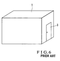
- Fig. 6 shows a conventional magnetic shield room. As shown in Fig. 6, a maintenance door 3 is provided to the side wall of a magnetic shield room 1, and a magnetic field shield material is adhered to the inner wall of the magnetic shield room 1. An EB exposure unit (not shown) or the like is arranged in the magnetic shield room 1.
- an opening portion having such a size that it does not allow the external magnetic field to influence the EB exposure unit may be formed in the magnetic shield room 1, and the cassette may be loaded/unloaded through this opening portion.
- the external magnetic shield enters the magnetic shield room 1 through the opening portion to adversely affect the EB exposure unit. Therefore, the EB exposure unit must be installed to be sufficiently remote from the opening. As a result, the area occupied by the magnetic shield room 1 with respect to the area occupied by the EB exposure unit becomes considerably large.
- the length of the short sides of the rectangular opening portion must be decreased to 100 mm or less. With this size, however, at most only one wafer or mask can be passed through this opening portion, and wafers and masks stored in a cassette cannot be loaded/unloaded at all.
- the length of the tubular member In order to sufficiently shield the external magnetic shield by providing a tube made of a magnetic shield material at the opening portion, the length of the tubular member must be increased in accordance with the size of the opening. If, however, the tubular member is long, it interferes with the operability of loading/unloading the cassette in/from the loading and unloading portions in the magnetic shield room. For example, when the operability of placing the cassette on the loading or unloading portion is considered, the length of the tubular member is preferably as small as possible.
- a shield lattice When a shield lattice is arranged in the tubular member, it is suitable for an application such as a vent port.
- the lattice interval For an application, e.g., a case that includes loading/unloading of a cassette, the lattice interval must be increased. For this reason, the length of the tubular member must be increased in accordance with the size of the opening, thus interfering with the operability.
- a magnetic shield apparatus comprising a magnetic shield room having an opening to shield external magnetism, a tubular member made of a magnetic shield material and attached to the opening to project from the magnetic shield room by a first predetermined length, and a flange portion made of a magnetic shield material and formed around a distal end portion of the tubular member to be spaced apart therefrom by a second predetermined length.
- a rectangular opening 120 is formed in the side surface of a magnetic shield room 101 having an inner wall adhered with a magnetic shield material.
- a tubular member 104 made of a magnetic shield material (e.g., permalloy) and having a rectangular section is attached to the opening 120 with rivets or the like.
- a portion of the tubular member 104 extending from its distal end for a predetermined length is outwardly bent at a right angle with respect to the tube axis to form a flange portion 105, as shown in Fig. 1B. More specifically, the flange portion 105 is constituted by the bent portions of the four sides of the distal end portion of the tubular member 104.
- An opening portion 102 is formed by the distal end portion of the tubular member 104 to communicate with the opening 120.
- the flange portion 105 is formed by bending the edges of the tubular member 104 outwardly and perpendicularly.
- the present invention is not limited to these values. It suffices if at least a portion of the tubular member 104 extending from its distal end for a predetermined length is inclined outwardly of the tubular member 104 at an angle of almost 90° with respect to the tube axis.
- the size d of the flange portion 105 may be set to 10 mm or more and the angle ⁇ of the flange portion 105 with respect to the tube axis may be set to 90°.
- a portion of the tubular member 104 near its distal end may be bent outwardly to have a certain radius of curvature, thereby forming a flange portion 205 having an arcuated section.
- a size d of the flange portion 205 may be set to 10 mm or more and an angle ⁇ formed by the tangential direction at the edge of the flange portion 205 and the tube axis may be set to 90°.
- the opening 120 is formed in one of the four side surfaces of the magnetic shield room 101.
- a magnetic shield material 111 is adhered to the entire inner wall of the magnetic shield room 101 without any gap to form a tubular member 104 projecting from the opening 120.
- a loading/unloading portion 106 for loading/unloading wafers or masks is arranged near the opening 120.
- a cassette loaded in the magnetic shield room 101 through the opening portion 102, the tubular member 104, and the opening 120 is mounted on the loading/unloading portion 106.
- the wafers and the like stored in the cassette are conveyed into a column 109 in an EB exposure unit 110 with an arm 107 of a convey arm portion 108, and are exposed. Thereafter, the exposed wafers are mounted on the cassette again by the arm 107 in an order reverse to that described above.
- the cassette mounted with the wafers is unloaded outside the magnetic shield room 101 through the opening 120, the tubular member 104, and the opening portion 102.
- the length of the tubular member 104 is preferably 200 mm or less.
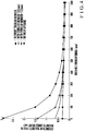
- Fig. 4 shows the relationship between the distance from the opening portion 102 and the strength of magnetic field in the magnetic shield room 101 when the external magnetic field has a strength of 5 mG.
- the magnetic field in the magnetic shield room 101 is 0.3 mG near the shield wall, 0.25 mG at a position separate from the shield wall by 500 mm, and 0.17 mG at a position separate from the shield wall by 1,000 mm, thus being attenuated gradually.
- the magnetic field near the opening 120 exhibits a value near about 3 mG but is 0.35 mG at a position separate from the opening 120 by 500 mm, thus being attenuated sharply. At a position farther separate from the opening 120, the magnetic field is attenuated gradually. However, even at a position separate from the opening 120 by 1,000 mm, the magnetic field has a strength of 0.23 mG, which is higher than the value obtained when the opening 120 is not formed by about 0.06 mG.
- the strength is 0.6 mG immediately inside the opening 120, but at a position separate from the opening 120 by 500 mm, the magnetic field is attenuated sharply to a value almost equal to that obtained when the opening 120 is not formed, and at a position separate from the opening 120 by 1,000 mm, the magnetic field is attenuated gradually to 0.17 mG.
- the tubular member 104 having no flange portion 105 when used, to obtain a shield effect almost equal to that described above, the tubular member 104 must have a length of 600 mm or more. This suggests effectiveness of the present invention in decreasing the length of the tubular member 104.
- the strength is about 1.4 mG immediately inside the opening 120, but at a position separate from the opening 120 by 500 mm, the magnetic field is attenuated sharply to a value almost equal to that obtained when the opening 120 is not formed, and at a position separate from the opening 120 by 1,000 mm, the magnetic field is attenuated gradually to 0.17 mG.
- the flange portion 105 may be formed by bending the edge of the distal end of the tubular member 104, as described above, or by mounting a rectangularly annular flange member 305 on flange-like edges 104a of the tubular member 104, shown in Fig. 5A, by using rivets 305a, as shown in Fig. 5B.
- the adhesion strength of the connecting portion can be increased. This decreases the impedance of the connecting portion so that the internal magnetic field can be emitted outside more easily.
- Connecting portions made of a magnetic shield material may be mounted to the notched portions between edges 104a of the tubular member 104 to connect the edges 104a to each other, thereby forming a flange portion continuously surrounding the opening portion 102 of the tubular member 104.
- no edges 104a may be formed on the tubular member 104, but a rectangularly annular flange member 305 made of a magnetic shield material may be attached to the distal end of the tubular member 104 with a known method.
- a tubular portion may be formed on the flange member 305 and be fixed to the tubular member 104 by fitting.
- strip segments made of a magnetic material and constituting a flange portion may be separately attached to the respective sides of the distal end portion of the tubular member 104.
- a tubular member having a flange portion is formed on the opening of a magnetic shield room. Even if the size of the opening is increased, the influence of the external magnetic field on the interior of the magnetic shield room can be decreased. More specifically, when compared to a case using only a tubular member, the same effect to that obtained by using a long tubular member can be obtained with a short tubular member. For example, when a tubular member having a flange portion and a length of about 100 mm is formed on the opening, the same effect as that obtained when no opening is formed can be obtained at a position separate from the opening by 500 mm. This allows loading/unloading of the cassette through the opening, and accordingly the loading/unloading portion can be arranged in the magnetic shield room, thus increasing the throughput.
- the distance between the EB exposure unit and the opening can be decreased. Since no extra space is required unlike in the conventional case, the magnetic shield room can be made compact.
Landscapes
- Engineering & Computer Science (AREA)
- Microelectronics & Electronic Packaging (AREA)
- Shielding Devices Or Components To Electric Or Magnetic Fields (AREA)
- Details Of Measuring And Other Instruments (AREA)
Applications Claiming Priority (2)
| Application Number | Priority Date | Filing Date | Title |
|---|---|---|---|
| JP9353051A JP2927284B2 (ja) | 1997-12-22 | 1997-12-22 | 磁気シールドルーム |
| JP35305197 | 1997-12-22 |
Publications (2)
| Publication Number | Publication Date |
|---|---|
| EP0924749A2 true EP0924749A2 (de) | 1999-06-23 |
| EP0924749A3 EP0924749A3 (de) | 2002-10-02 |
Family
ID=18428244
Family Applications (1)
| Application Number | Title | Priority Date | Filing Date |
|---|---|---|---|
| EP98124436A Withdrawn EP0924749A3 (de) | 1997-12-22 | 1998-12-22 | Vorrichtung zur magnetischen Abschirmung |
Country Status (6)
| Country | Link |
|---|---|
| US (1) | US6265723B1 (de) |
| EP (1) | EP0924749A3 (de) |
| JP (1) | JP2927284B2 (de) |
| KR (1) | KR100306986B1 (de) |
| CN (1) | CN1114341C (de) |
| TW (1) | TW398166B (de) |
Families Citing this family (10)
| Publication number | Priority date | Publication date | Assignee | Title |
|---|---|---|---|---|
| JP4150493B2 (ja) * | 2000-08-22 | 2008-09-17 | 株式会社東芝 | パターン描画装置における温度測定方法 |
| CA2359597C (en) * | 2001-10-23 | 2003-10-21 | Roland Kenny | Beverage can holder |
| US6962644B2 (en) | 2002-03-18 | 2005-11-08 | Applied Materials, Inc. | Tandem etch chamber plasma processing system |
| JP2003309393A (ja) * | 2002-04-12 | 2003-10-31 | Fujita Corp | 磁気シールド構造およびその設計法 |
| US20030230385A1 (en) * | 2002-06-13 | 2003-12-18 | Applied Materials, Inc. | Electro-magnetic configuration for uniformity enhancement in a dual chamber plasma processing system |
| JP4782646B2 (ja) * | 2006-08-25 | 2011-09-28 | 株式会社竹中工務店 | 多層磁気シールドルーム |
| JP2012074457A (ja) * | 2010-09-28 | 2012-04-12 | Igarashi Chikara | 磁気シールド補助装置及び磁気シールドシステム |
| WO2014192379A1 (ja) * | 2013-05-30 | 2014-12-04 | 株式会社 日立ハイテクノロジーズ | 荷電粒子線装置 |
| US10104816B2 (en) * | 2016-02-05 | 2018-10-16 | Taiwan Semiconductor Manufacturing Co., Ltd. | Board, semiconductor fabrication plant (FAB) and fabrication facility |
| CN112858963B (zh) * | 2021-03-02 | 2025-05-16 | 中国科学院高能物理研究所 | 一种磁屏蔽腔体、测量系统及测量方法 |
Family Cites Families (5)
| Publication number | Priority date | Publication date | Assignee | Title |
|---|---|---|---|---|
| US4482811A (en) * | 1982-09-30 | 1984-11-13 | Radiation Dynamics, Inc. | Apparatus for guiding cable through a radiation chamber with reduced leakage therefrom |
| JPS59197198A (ja) | 1983-04-22 | 1984-11-08 | 株式会社トーキン | 磁気シ−ルド装置 |
| JPS6457700A (en) | 1987-08-28 | 1989-03-03 | Hitachi Ltd | Magnetic shielding device |
| JP2744470B2 (ja) | 1989-06-09 | 1998-04-28 | 出光興産株式会社 | 潤滑油組成物 |
| JPH07122886A (ja) | 1993-10-22 | 1995-05-12 | Shimizu Corp | 磁気シールドルームにおける出入口開口部 |
-
1997
- 1997-12-22 JP JP9353051A patent/JP2927284B2/ja not_active Expired - Fee Related
-
1998
- 1998-12-17 TW TW087121103A patent/TW398166B/zh active
- 1998-12-22 KR KR1019980057193A patent/KR100306986B1/ko not_active Expired - Fee Related
- 1998-12-22 EP EP98124436A patent/EP0924749A3/de not_active Withdrawn
- 1998-12-22 US US09/218,501 patent/US6265723B1/en not_active Expired - Fee Related
- 1998-12-22 CN CN98125866A patent/CN1114341C/zh not_active Expired - Fee Related
Also Published As
| Publication number | Publication date |
|---|---|
| CN1114341C (zh) | 2003-07-09 |
| CN1224328A (zh) | 1999-07-28 |
| EP0924749A3 (de) | 2002-10-02 |
| KR100306986B1 (ko) | 2002-02-19 |
| JP2927284B2 (ja) | 1999-07-28 |
| KR19990063318A (ko) | 1999-07-26 |
| US6265723B1 (en) | 2001-07-24 |
| TW398166B (en) | 2000-07-11 |
| JPH11186779A (ja) | 1999-07-09 |
Similar Documents
| Publication | Publication Date | Title |
|---|---|---|
| US6265723B1 (en) | Magnetic shield apparatus | |
| US7157703B2 (en) | Electron beam system | |
| EP1119022B1 (de) | Vakuumbehandlungsanlage und Halbleiterfertigungsstrasse die diese verwendet | |
| TWI404151B (zh) | 檢測裝置及檢查裝置 | |
| KR20010092264A (ko) | 포오트 출입구의 유지 및 배출 시스템 | |
| US20040187786A1 (en) | Processing apparatus for processing sample in predetermined atmosphere | |
| JP2001509647A (ja) | 真空処理システムにおける2ピース式スリットバルブインサート | |
| US20020134506A1 (en) | Transfer chamber with side wall port | |
| US7361600B2 (en) | Semiconductor manufacturing apparatus having a built-in inspection apparatus and a device manufacturing method using said manufacturing apparatus | |
| US10290522B2 (en) | Conductive interface system between vacuum chambers in a charged particle beam device | |
| US20080067368A1 (en) | Ionizing system for vacuum process and metrology equipment | |
| US20250170623A1 (en) | Vacuum Processing Device and Foreign Matter Ejection Method | |
| US20040147122A1 (en) | Wafer processing apparatus having dust proof function | |
| JP5030410B2 (ja) | 真空処理装置 | |
| US5900047A (en) | Exhaust system for a semiconductor etcher that utilizes corrosive gas | |
| JPH11162838A (ja) | 半導体製造装置およびチャンバ | |
| JPH10189682A (ja) | 真空処理装置 | |
| US6054014A (en) | Exhaust apparatus | |
| JP2003209149A (ja) | 検査装置を内蔵する半導体製造装置および該製造装置を用いるデバイス製造方法 | |
| JP2001085290A (ja) | 半導体露光装置とデバイス製造方法 | |
| EP4423571A1 (de) | Innen-pod-dichtungsspalt für extremes uv | |
| JPH07148582A (ja) | イオンビーム加工装置 | |
| JPH05106041A (ja) | 真空装置 | |
| KR20030006825A (ko) | 웨이퍼 카세트에 부착되는 바코드를 판별할 수 있는로드락 챔버 | |
| KR20210088778A (ko) | 로드 포트 유닛, 이를 포함하는 저장 장치 및 배기 방법 |
Legal Events
| Date | Code | Title | Description |
|---|---|---|---|
| PUAI | Public reference made under article 153(3) epc to a published international application that has entered the european phase |
Free format text: ORIGINAL CODE: 0009012 |
|
| AK | Designated contracting states |
Kind code of ref document: A2 Designated state(s): AT BE CH CY DE DK ES FI FR GB GR IE IT LI LU MC NL PT SE |
|
| AX | Request for extension of the european patent |
Free format text: AL;LT;LV;MK;RO;SI |
|
| PUAL | Search report despatched |
Free format text: ORIGINAL CODE: 0009013 |
|
| AK | Designated contracting states |
Kind code of ref document: A3 Designated state(s): AT BE CH CY DE DK ES FI FR GB GR IE IT LI LU MC NL PT SE |
|
| AX | Request for extension of the european patent |
Free format text: AL;LT;LV;MK;RO;SI |
|
| RIC1 | Information provided on ipc code assigned before grant |
Free format text: 7H 01L 21/00 A, 7H 05K 9/00 B |
|
| 17P | Request for examination filed |
Effective date: 20020827 |
|
| RAP1 | Party data changed (applicant data changed or rights of an application transferred) |
Owner name: NEC ELECTRONICS CORPORATION |
|
| AKX | Designation fees paid |
Designated state(s): DE FR GB NL |
|
| STAA | Information on the status of an ep patent application or granted ep patent |
Free format text: STATUS: THE APPLICATION HAS BEEN WITHDRAWN |
|
| 18W | Application withdrawn |
Effective date: 20030917 |