EP0924859B1 - Circuit logique avec génération d'horloge propre et procédé associé - Google Patents
Circuit logique avec génération d'horloge propre et procédé associé Download PDFInfo
- Publication number
- EP0924859B1 EP0924859B1 EP98304052A EP98304052A EP0924859B1 EP 0924859 B1 EP0924859 B1 EP 0924859B1 EP 98304052 A EP98304052 A EP 98304052A EP 98304052 A EP98304052 A EP 98304052A EP 0924859 B1 EP0924859 B1 EP 0924859B1
- Authority
- EP
- European Patent Office
- Prior art keywords
- signal
- delay
- bits
- period
- input
- Prior art date
- Legal status (The legal status is an assumption and is not a legal conclusion. Google has not performed a legal analysis and makes no representation as to the accuracy of the status listed.)
- Expired - Lifetime
Links
- 238000000034 method Methods 0.000 title claims description 14
- 230000003111 delayed effect Effects 0.000 claims description 30
- 230000004044 response Effects 0.000 claims description 14
- 230000006870 function Effects 0.000 description 15
- 230000001360 synchronised effect Effects 0.000 description 7
- 238000010586 diagram Methods 0.000 description 6
- 230000001934 delay Effects 0.000 description 4
- 238000004519 manufacturing process Methods 0.000 description 2
- 239000004065 semiconductor Substances 0.000 description 2
- 239000013078 crystal Substances 0.000 description 1
- 238000012986 modification Methods 0.000 description 1
- 230000004048 modification Effects 0.000 description 1
- 238000012544 monitoring process Methods 0.000 description 1
- 238000005070 sampling Methods 0.000 description 1
- 239000000758 substrate Substances 0.000 description 1
Images


Classifications
-
- H—ELECTRICITY
- H03—ELECTRONIC CIRCUITRY
- H03K—PULSE TECHNIQUE
- H03K3/00—Circuits for generating electric pulses; Monostable, bistable or multistable circuits
- H03K3/02—Generators characterised by the type of circuit or by the means used for producing pulses
- H03K3/027—Generators characterised by the type of circuit or by the means used for producing pulses by the use of logic circuits, with internal or external positive feedback
- H03K3/037—Bistable circuits
- H03K3/0375—Bistable circuits provided with means for increasing reliability; for protection; for ensuring a predetermined initial state when the supply voltage has been applied; for storing the actual state when the supply voltage fails
Definitions
- the present invention relates to logic circuits such as sequential logic circuits and, more particularly, to a novel circuit and method for clocking a logic circuit.
- a salient feature of sequential logic circuits is memory.
- the output of a sequential logic circuit depends not only on the current values of applied input signals but also on the past circuit state, e.g. the sequence of previously applied input signals.
- Sequential logic circuits can be asynchronous or synchronous.
- Asynchronous sequential circuits respond immediately to changes in input signals, yielding changed output signals.
- unequal propagation delays in asynchronous circuits can lead to hazards and race conditions.
- synchronous circuits are employed in which signals are latched into registers in response to regular clock pulses.
- the speed of synchronous circuits is constrained by the period of the clock cycles, which depends on the propagation delays of logic blocks and registers.
- Figure 3 depicts a synchronous circuit including two blocks of combinational logic: a first logic block 302 for computing a function "F" based on "N" inputs I 1 -I N and a second logic block 306 for computing a function "G” based on "M” inputs F 1 -F M .
- the circuit also includes three registers 300 , 304 , and 308 for latching bits at the beginning of each clock cycle.
- the bits F 1 -F M are latched by register 304 , they are applied the second logic block 306 .
- the second logic block 306 computes the function "G” based on the bits F 1 -F M and produces therefrom "L” bits of output G 1 -G L .
- These output bits G 1 -G L are applied to register 306 and latched in response to the clock signal at the next clock cycle.
- the computation of functions "F” and "G” takes two clock cycles to complete.
- registers 300 , 304, and 308 have a propagation delay of 7ns
- the first logic block 302 has a propagation delay of 21ns
- the second logic block 306 has a propagation delay of 28ns.
- the computation in the first clock cycle needs at least 28ns to complete (7ns for the register 300 to latch + 21ns for first logic block 302 ).
- the computation in the second clock cycle requires at least 35ns to complete before the data is ready to be latched by register 308 (7ns for the register 304 + 28ns for the second logic block 306 ). Since registers 300, 304, and 308 share a common clock signal, the clock period is set to 35ns.
- the total time taken to perform the two computations i.e. two clock cycles, is 70ns.
- 7ns of the first clock period of 35ns was spent waiting for the next clock cycle. Therefore, digital functions are conventionally cascaded at the speed of the common clock, which is slower than cascading at the speed of most of the functions themselves.
- US-A-5, 229,668 discloses method and apparatus for high speed digital sampling of a data signal.
- US-A-5,033,066 discloses a time delay circuit for providing a delayed replica of a digital input signal.
- GB-A-2,310,738 discloses a dynamic logic pipeline in which each stage has a logic circuit, a latch circuit and a control circuit.
- US-A-5,565,798 discloses a self-timed control circuit for self-resetting logic circuitry.
- each input into a logic block or circuit is associated with a validity signal.
- the validity signal is delayed by a delay line for at least, but preferably within 140ns of, the propagation delay of the logic block.
- the delayed validity signal can be used to latch an output signal produced from the logic block in response to the inputs.
- one aspect of the invention is a sequential logic circuit, comprising:
- Another aspect of the present invention is a method of latching an output signal generated by a logic circuit in response to an input signal after a delay, the input signal including a plurality of input bits; said method being characterized by comprising the steps of:
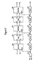
- Figure 1 depicts a self-clocked sequential circuit corresponding to the conventional sequential circuit depicted in Figure 3.
- logic blocks 102 and 106 of Figure 1 correspond to logic blocks 302 and 306 of Figure 3, respectively.
- Registers 100 , 104 , and 108 of Figure 1 correspond to registers 300 , 304 , and 308 of Figure 3, respectively.
- first logic block 102 computes the function "F” based on “N” inputs I 1 -I N
- second logic block 106 computes the function "G” based on "M” inputs F 1 -F M .
- the three registers 100, 104, and 108 latch bits applied thereto in response to the signals generated by the self-clocking circuitry including delay lines 110-118 and gate 120 .
- each bit of the input signal I 1 -I N is a corresponding validity bit VI 1 -VI N that is asserted when the associated input bit I 1 -I N is valid.
- the validity bits VI 1 -VI N may be produced asynchronously or synchronously when the input signal I 1 -I N is first received from another circuit, e.g. an off-chip circuit. For example, some input signals are transmitted to an integrated circuit with a strobe that indicates that the inputs are ready. In this situation, the associated validity signal is derived from the strobe. In another example, the input signals are valid at every cycle of an externally supplied clock signal, in which case the associated validity signal would be derived from the clock signal.
- Validity signals associated with signals generated by internal, i.e. on-chip, logic blocks are derived from the self-clocking circuitry for respective internal logic blocks.
- the self-clocking circuitry includes a gate 120, which determines when all the input bits I 1 -I N for the corresponding register 100 are valid, i.e. when all the validity bits VI 1 -VI N have been asserted.
- Gate 120 can be any circuitry which computes a logical product, such as an AND gate in positive logic or a NOR gate in negative logic.
- the output of gate 120 is coupled to the "CLOCK" input of register 100 , so that, when all the validity bits VI 1 -VI N have been asserted, the resultant, consolidated input validity signal VI causes the register 100 to latch the input bits I 1 -I N . Thus, the input bits I 1 -I N are latched only when all of the input bits I 1 -I N are valid.
- the output of gate 120 is coupled to a delay line 110 , which may be implemented as described in more detail hereinbelow.
- the input validity signal VI is delayed by delay line 110 , configured to delay the input validity signal VI for a period of time at least as long as the propagation delay for the register 100 . For example, if the register 100 has a propagation delay of 7ns, then the delay line 100 would be configured to delay the input validity signal VI for at least 7ns to produce a delayed input validity signal VI' .
- the first logic block 102 computes the function "F" on the input bits and produces therefrom "M" bits of output F 1 -F M after some propagation delay. Meanwhile, the corresponding delayed input validity signal VI' for the input bits I 1 -I N is delayed by delay line 112, configured to delay the delayed input validity signal VI' for a period of time at least as long as the propagation delay of the first logic block 102. Thus, the output of the delay line 112 is asserted when the outputs of the corresponding first logic block 102 become valid. In other words, the output of the delay line 112 is a validity signal VF for the first logic block 102. In the example, if the first logic block 102 has a propagation delay of 21ns, then the delay line 112 would be configured to delay the delayed input validity signal VI' for at least 21ns to produce the first block validity signal VF.
- the first block validity signal VF is produced by delay line 112 when the bits F 1 -F M are valid, the first block validity signal VF is used to latch the bits F 1 -F M at the register 104. After the bits F 1 -F M are latched by register 304, they are applied the second logic block 306 after a propagation delay. Meanwhile, the first block validity signal VF is delayed by delay line 114 , configured to delay the first block validity signal VF for a period of time at least as long as the propagation delay for the register 104 . In the example, if the register 104 has a propagation delay of 7ns, then the delay line 114 would be configured to delay the first block validity signal VF for at least 7ns to produce a delayed first block validity signal VF' .
- the second logic block 106 computes the function "G" based on the bits F 1 -F M applied thereto and produces therefrom "L" bits of output G 1 -G L after a propagation delay. Meanwhile, the corresponding delayed first block validity signal VF' for the bits F 1 -F M is delayed by delay line 116 , configured to delay the delayed first block validity signal VF' for a period of time at least as long as the propagation delay of the second logic block 106 . Thus, the output of the delay line 116 is asserted when the outputs of the corresponding second logic block 106 become valid. In other words, the output of the delay line 116 is a validity signal VG for the second logic block 106 . In the example, if the second logic block 106 has a propagation delay of 28ns, then the delay line 116 would be configured to delay the delayed first block validity signal VF' for at least 28ns to produce the second block validity signal VG .
- delay line 116 is coupled to the "CLOCK" input of register 108 , the output bits G 1 -G L are latched by register 106 in response to the second block validity signal VG .
- the second block validity signal VG is delayed by delay line 118 , configured to delay the second block validity signal VG for a period of time at least as long as the propagation delay for the register 108 .
- the delay line 118 would be configured to delay the second block validity signal VG for at least 7ns to produce a delayed second block validity signal VG' .
- the time elapsed from when the input bits I 1 -I N have become valid at register 100 until when the output bits G 1 -G L are ready at register 108 is the sum of the propagation delays through first logic block 102 , second logic block 106 , and registers 100 and 104 .
- the register latching the output of a faster logic block is configured to latch the output immediately without having to wait a period of time synchronized with the a slower logic block (e.g. second logic block 106 ).
- Figure 2(a) is a block diagram of an exemplary high-resolution, digital delay line 200 with which the present invention can be implemented.
- the exemplary high-resolution digital delay line 200 receives a bit and repeatedly delays the bit through a plurality of digital delay elements 210-1 to 210-n , coupled in series.
- Digital delay line 200 may comprise an arbitrary number n of digital delay elements, depending upon any constraints inherent in the semiconductor implementation utilized or other practical considerations.
- digital delay line 200 can comprise tens of thousands of digital delay elements. Since each of the digital delay elements 210-1 to 210-n of digital delay line 200 is constructed during the same manufacturing process on the same semiconductor substrate, it is likely that the operating characteristics, and hence the delay period, of each digital delay element are nearly identical.
- digital delay line 200 comprises a plurality of taps 212-1 to 212-n coupled to the outputs of the respective digital delay elements 210-1 to 210-n for monitoring portions of the digital delay line 200 in parallel.
- Delay characteristics of any digital circuit will vary from chip to chip and over time because of unavoidable variations in manufacturing and operating conditions.
- both the delay period is synchronized to a reliable, precise reference clock, such as a crystal oscillator.
- the delay period of each of the digital delay elements 210-1 to 210-n is preferably adjustable by a digital command code as a calibration signal.
- This calibration signal is produced with reference to a reliable, precise clock signal, preferably by an on-chip digital servo circuit (not shown) such as described in the commonly assigned U.S. Patent No. 5,457,719, issued to Guo et al. on October 10, 1995.
- the on-chip digital servo circuit comprises an adjustable digital delay line of its own, which it monitors and continually adjusts with a calibration signal in a feedback loop.
- the calibration signal is shared with other systems on the chip.
- each adjustable digital delay element 210 comprises two adjustable inverters 220-1 and 220-2 , coupled in series, each receiving the aforementioned calibration signal.
- the delay period of each of the two adjustable inverters 220-1 and 220-2 is one-half of the delay period of the adjustable delay element and is controlled by the calibration signal.
- each adjustable inverter 220 in a preferred embodiment comprises a plurality of switchable inverters 230-1 to 230-m coupled in parallel.
- Each of the switchable inverters 230-1 to 230-m is switched on or off by one of bits 232-1 to 232-m of the calibration signal.
- two of the parameters that determine the propagation delay of an inverter, the P-channel size to N-channel size ratio and the driving power may be determined for precise control over the delay period.
- Switchable inverters are described in further detail in the commonly assigned U.S. Patent No. 5,220,216, issued to Woo on June 15, 1993, and the commonly assigned U.S. Patent No. 5,227,679, issued to Woo on July 13, 1993.
- digital delay line 200 comprises a series of adjustable digital delay elements 210-1 to 210-n , each of which provides a uniform delay period synchronized to a reference clock period according to a calibration signal.
- each adjustable inverter 220 can have a consistent delay period of as little as 70 ps.
- each adjustable digital delay element 210 can have a consistent delay period of as little as 140 ps.
- the digital delay line 200 is implemented with enough adjustable digital delay elements of a particular delay period so that the total delay period exceeds'the delay time of the worst case path through the corresponding logic circuit. For example, if the delay time of the worst case path through the logic circuit is 28ns, then a minimum of 200 (28 ns / 140 ps) adjustable delay elements having a 140 ps delay period is required. Thus, digital delay line 200 can be configured to delay a signal within 140ps of a desired delay period.
- adjustable delay elements can be reduced by using adjustable delay elements with a larger period.
- adjustable delay elements having different periods may be used, for example nineteen with a delay period of 1.4ns and ten with a delay period of 140ps.
- the series of delay lines 110-118 ultimately delay a single validity signal, viz. VI . Accordingly, the series of delay lines 110-118 may be replaced with a single delay line having appropriate taps coupled to respective "CLOCK" inputs of registers 104 and 108 .
Landscapes
- Pulse Circuits (AREA)
- Shift Register Type Memory (AREA)
Claims (15)
- Circuit logique séquentiel comprenant :caractérisé en ce que le circuit séquentiel est à génération d'horloge propre comprenant, de plus :un circuit logique (102) répondant à un signal d'entrée (I1 - In) pour calculer une fonction à partir de lui et produire un signal de sortie (F1 - Fm) après un délai de propagation, ledit signal d'entrée (I1 - In) incluant une pluralité de bits d'entrée ; etun registre (104) pour verrouiller ledit signal de sortie (F1-Fm) ;une ligne à retard (120, 110, 112) répondant à un premier signal (VI1 - VIn) pour fournir un premier signal retardé (VF) après un laps de temps au moins aussi long que ledit délai de propagation, ledit premier signal (VI1 - VIn) comportant le même nombre de bits que ledit signal d'entrée (I1 - In), chaque bit dudit premier signal (VI1-VIn) correspondant, respectivement, à un bit dudit signal d'entrée (I1-In) et présentant une valeur commune de bit spécifiée lorsque le bit correspondant dudit signal d'entrée (I1 - In) est reçu en premier par ledit circuit logique séquentiel, ladite ligne à retard (120, 110, 112) comportant un circuit (120) pour calculer un produit logique sur ladite pluralité de bits dudit premier signal (VI1 - VIn) et étant agencée pour produire ledit premier signal retardé (VF) après un laps de temps au moins aussi long que ledit délai de propagation lorsque tous les bits de la pluralité de bits dudit premier signal (VI1-VIn) sont à la valeur commune de bit spécifiée, et ledit registre (104) verrouillant ledit signal de sortie (F1 - Fm) en réponse audit premier signal retardé (VF).
- Circuit à génération d'horloge propre selon la revendication 1, dans lequel ledit circuit servant à calculer un produit logique comporte une porte ET (120) répondant à ladite pluralité de bits dudit premier signal (VI1 - VIn).
- Circuit à génération d'horloge propre selon la revendication 1, dans lequel ledit circuit servant à calculer un produit logique comporte une porte NON-OU (120) répondant à ladite pluralité de bits dudit premier signal (VI1 - VIn).
- Circuit à génération d'horloge propre selon l'une quelconque des revendications 1 à 3 comprenant, de plus, une autre ligne à retard (114) répondant audit premier signal retardé (VF) pour générer un second signal retardé (VF') après un laps de temps aussi long au moins qu'un temps de retard dudit registre (104).
- Circuit à génération d'horloge propre selon l'une quelconque des revendications 1 à 4, dans lequel ladite ligne à retard (120, 110, 112) est agencée pour produire ledit premier signal retardé (VF) dans les 140ps dudit délai de propagation.
- Circuit à génération d'horloge propre selon l'une quelconque des revendications 1 à 4, dans lequel ladite ligne à retard (120, 110, 112) et/ou ladite autre ligne à retard (114) comporte une pluralité d'éléments à retard numériques (210-1 à 210-n) couplés en série.
- Circuit à génération d'horloge propre selon la revendication 6, dans lequel :ladite ligne à retard et/ou ladite autre ligne à retard comprend, de plus, une entrée de calibrage couplée pour recevoir un signal de calibrage (CALIBRATE) ; etchacun des éléments à retard numériques (210-1 à 210-n) comprend une entrée de calibrage (CALIBRATE) pour recevoir le signal de calibrage servant à régler son temps de retard.
- Circuit à génération d'horloge propre selon la revendication 7, dans lequel chacun des éléments à retard numériques (210-1 à 210-n) comprend :un premier inverseur réglable (220-1) comportant une première entrée de calibrage pour recevoir le signal de calibrage (CALIBRATE) ; etun second inverseur réglable (220-2), couplé en série audit premier inverseur réglable (220-1) et comportant une seconde entrée de calibrage pour recevoir ledit signal de calibrage (CALIBRATE).
- Circuit à génération d'horloge propre selon l'une quelconque des revendications 1 à 8 dans lequel un temps de retard de chacun des éléments à retard numériques dure environ 140 ps.
- Circuit à génération d'horloge propre selon l'une quelconque des revendications 1 à 9 dans lequel le temps de retard de chacun des éléments à retard numériques est le même.
- Procédé de verrouillage d'un signal de sortie (F1 - Fm) généré par un circuit logique (102) en réponse à un signal d'entrée (I1 - In) après un retard (112), ledit signal d'entrée comprenant une pluralité de bits d'entrée (I1 - In), ledit procédé étant
caractérisé en ce qu'il comprend les étapes consistant à :fournir un premier signal (VI1 -VIn) comportant le même nombre de bits que ledit signal d'entrée (I1 - In), chaque bit dudit premier signal (VI1 - VIn) correspondant respectivement à un bit dudit signal d'entrée (I1 - In) et ayant une valeur commune de bit spécifiée lorsque le bit correspondant dudit signal d'entrée (I1 - In) est reçu en premier par ledit circuit logique séquentiel ;calculer un produit logique sur ladite pluralité de bits dudit premier signal (VI1-VIn) etdélivrer un second signal (VI) lorsque chacun des bits dudit premier signal (VI1 - VIn) présente la valeur commune de bit spécifiée ;retarder (110, 112) ledit second signal (VI) pendant un laps de temps au moins aussi long que ledit temps de retard ; etverrouiller (104) ledit signal de sortie (F1 - Fm) en réponse audit second signal retardé (VF). - Procédé selon la revendication 11 comprenant, de plus, l'étape consistant à retarder le second signal retardé (VF) pendant un autre laps de temps (114) qui dure au moins aussi longtemps que ladite étape de verrouillage.
- Procédé selon l'une quelconque des revendications 11 et 12 dans lequel le retard dudit second signal pour un laps de temps au moins aussi long que ledit temps de retard comprend l'étape consistant à retarder ledit second signal dans les 140ps dudit temps de retard.
- Procédé selon l'une quelconque des revendications 11 à 13 dans lequel l'étape consistant à retarder ledit second signal pendant un laps de temps au moins aussi long que ledit temps de retard comprend l'étape consistant à retarder de façon répétée ledit second signal d'une période de retard commune (210-1 à 210-n).
- Procédé selon la revendication 14 comprenant, de plus, l'étape consistant à calibrer (CALIBRATE) ladite période de retard commune.
Applications Claiming Priority (2)
| Application Number | Priority Date | Filing Date | Title |
|---|---|---|---|
| US992634 | 1997-12-18 | ||
| US08/992,634 US6064232A (en) | 1997-12-18 | 1997-12-18 | Self-clocked logic circuit and methodology |
Publications (2)
| Publication Number | Publication Date |
|---|---|
| EP0924859A1 EP0924859A1 (fr) | 1999-06-23 |
| EP0924859B1 true EP0924859B1 (fr) | 2004-02-04 |
Family
ID=25538564
Family Applications (1)
| Application Number | Title | Priority Date | Filing Date |
|---|---|---|---|
| EP98304052A Expired - Lifetime EP0924859B1 (fr) | 1997-12-18 | 1998-05-21 | Circuit logique avec génération d'horloge propre et procédé associé |
Country Status (4)
| Country | Link |
|---|---|
| US (1) | US6064232A (fr) |
| EP (1) | EP0924859B1 (fr) |
| JP (1) | JPH11185492A (fr) |
| DE (1) | DE69821461T2 (fr) |
Cited By (1)
| Publication number | Priority date | Publication date | Assignee | Title |
|---|---|---|---|---|
| TWI783425B (zh) * | 2020-06-04 | 2022-11-11 | 大陸商深圳比特微電子科技有限公司 | 時鐘電路、計算晶片、算力板和資料處理設備 |
Families Citing this family (13)
| Publication number | Priority date | Publication date | Assignee | Title |
|---|---|---|---|---|
| US6232796B1 (en) * | 1999-07-21 | 2001-05-15 | Rambus Incorporated | Apparatus and method for detecting two data bits per clock edge |
| US6369614B1 (en) * | 2000-05-25 | 2002-04-09 | Sun Microsystems, Inc. | Asynchronous completion prediction |
| JP2002083000A (ja) * | 2000-09-06 | 2002-03-22 | Fujitsu Ltd | 論理回路設計方法及び論理回路 |
| US6621302B2 (en) * | 2001-03-21 | 2003-09-16 | Bae Systems Information And Electronic Systems Integration, Inc | Efficient sequential circuits using critical race control |
| US6731147B2 (en) | 2001-10-29 | 2004-05-04 | Cypress Semiconductor Corp. | Method and architecture for self-clocking digital delay locked loop |
| US20050151570A1 (en) * | 2002-02-21 | 2005-07-14 | Van Lammeren Johannes P.M. | Integrated circuit having reduced substate bounce |
| CN1879171B (zh) * | 2003-11-12 | 2012-04-25 | Nxp股份有限公司 | 控制电子电路中的功耗峰值 |
| DE102005033270B4 (de) * | 2005-07-15 | 2007-11-29 | Texas Instruments Deutschland Gmbh | Digitale Logikeinheit |
| US7671579B1 (en) * | 2006-03-09 | 2010-03-02 | Altera Corporation | Method and apparatus for quantifying and minimizing skew between signals |
| US8543750B1 (en) | 2008-10-15 | 2013-09-24 | Octasic Inc. | Method for sharing a resource and circuit making use of same |
| US8689218B1 (en) * | 2008-10-15 | 2014-04-01 | Octasic Inc. | Method for sharing a resource and circuit making use of same |
| US8130019B1 (en) * | 2008-10-15 | 2012-03-06 | Octasic Inc. | Clock signal propagation method for integrated circuits (ICs) and integrated circuit making use of same |
| US9602106B1 (en) * | 2015-03-05 | 2017-03-21 | Altera Corporation | Methods for optimizing circuit performance via configurable clock skews |
Citations (2)
| Publication number | Priority date | Publication date | Assignee | Title |
|---|---|---|---|---|
| US5565798A (en) * | 1995-08-21 | 1996-10-15 | International Business Machines Corporation | Self-timed control circuit for self-resetting logic circuitry |
| GB2310738A (en) * | 1996-02-29 | 1997-09-03 | Advanced Risc Mach Ltd | Latching in dynamic logic pipelines |
Family Cites Families (21)
| Publication number | Priority date | Publication date | Assignee | Title |
|---|---|---|---|---|
| US4929850A (en) * | 1987-09-17 | 1990-05-29 | Texas Instruments Incorporated | Metastable resistant flip-flop |
| US5033066A (en) * | 1990-02-16 | 1991-07-16 | Hughes Aircraft Company | Event tagging time delay |
| EP0453171A3 (en) * | 1990-04-18 | 1992-11-19 | Quickturn Systems Inc | Method for substantially eliminating hold time violations in implementing high speed logic circuits or the like |
| US5111086A (en) * | 1990-11-19 | 1992-05-05 | Wang Laboratories, Inc. | Adjusting delay circuitry |
| JPH0528789A (ja) * | 1991-07-25 | 1993-02-05 | Sharp Corp | 論理回路 |
| US5132572A (en) * | 1991-08-12 | 1992-07-21 | Advanced Micro Devices, Inc. | High-speed CMOS-to-ECL translator circuit |
| DE4137340C1 (en) * | 1991-11-13 | 1992-11-26 | Siemens Ag, 8000 Muenchen, De | Bistable flip=flop circuit comprising two D=flip=flops and correction circuit - checks output level of first flip=flop and uses correction signal to switch through output of flip=flop or reference signal to second flip=flop |
| US5227679A (en) * | 1992-01-02 | 1993-07-13 | Advanced Micro Devices, Inc. | Cmos digital-controlled delay gate |
| US5220216A (en) * | 1992-01-02 | 1993-06-15 | Woo Ann K | Programmable driving power of a CMOS gate |
| US5252867A (en) * | 1992-02-14 | 1993-10-12 | Vlsi Technology, Inc. | Self-compensating digital delay semiconductor device with selectable output delays and method therefor |
| DE4206082C1 (fr) * | 1992-02-27 | 1993-04-08 | Siemens Ag, 8000 Muenchen, De | |
| US5229668A (en) * | 1992-03-25 | 1993-07-20 | North Carolina State University Of Raleigh | Method and apparatus for high speed digital sampling of a data signal |
| US5363419A (en) * | 1992-04-24 | 1994-11-08 | Advanced Micro Devices, Inc. | Dual phase-locked-loop having forced mid range fine control zero at handover |
| US5452333A (en) * | 1992-06-19 | 1995-09-19 | Advanced Micro Devices, Inc. | Digital jitter correction method and signal preconditioner |
| US5367542A (en) * | 1992-06-19 | 1994-11-22 | Advanced Micro Devices, Inc. | Digital data recovery using delay time rulers |
| US5349612A (en) * | 1992-06-19 | 1994-09-20 | Advanced Micro Devices, Inc. | Digital serializer and time delay regulator |
| US5264745A (en) * | 1992-08-28 | 1993-11-23 | Advanced Micro Devices, Inc. | Recovering phase and data from distorted duty cycles caused by ECL-to-CMOS translator |
| US5400370A (en) * | 1993-02-24 | 1995-03-21 | Advanced Micro Devices Inc. | All digital high speed algorithmic data recovery method and apparatus using locally generated compensated broad band time rulers and data edge position averaging |
| US5457719A (en) * | 1993-08-11 | 1995-10-10 | Advanced Micro Devices Inc. | All digital on-the-fly time delay calibrator |
| US5457336A (en) * | 1994-10-13 | 1995-10-10 | Advanced Micro Devices, Inc. | Non-volatile memory structure including protection and structure for maintaining threshold stability |
| US5764083A (en) * | 1996-06-10 | 1998-06-09 | International Business Machines Corporation | Pipelined clock distribution for self resetting CMOS circuits |
-
1997
- 1997-12-18 US US08/992,634 patent/US6064232A/en not_active Expired - Fee Related
-
1998
- 1998-05-21 DE DE69821461T patent/DE69821461T2/de not_active Expired - Lifetime
- 1998-05-21 EP EP98304052A patent/EP0924859B1/fr not_active Expired - Lifetime
- 1998-06-22 JP JP10174641A patent/JPH11185492A/ja not_active Withdrawn
Patent Citations (2)
| Publication number | Priority date | Publication date | Assignee | Title |
|---|---|---|---|---|
| US5565798A (en) * | 1995-08-21 | 1996-10-15 | International Business Machines Corporation | Self-timed control circuit for self-resetting logic circuitry |
| GB2310738A (en) * | 1996-02-29 | 1997-09-03 | Advanced Risc Mach Ltd | Latching in dynamic logic pipelines |
Cited By (2)
| Publication number | Priority date | Publication date | Assignee | Title |
|---|---|---|---|---|
| TWI783425B (zh) * | 2020-06-04 | 2022-11-11 | 大陸商深圳比特微電子科技有限公司 | 時鐘電路、計算晶片、算力板和資料處理設備 |
| US12248334B2 (en) | 2020-06-04 | 2025-03-11 | Shenzhen Microbt Electronics Technology Co., Ltd. | Clock circuits, computing chips, hash boards and data processing devices |
Also Published As
| Publication number | Publication date |
|---|---|
| US6064232A (en) | 2000-05-16 |
| JPH11185492A (ja) | 1999-07-09 |
| EP0924859A1 (fr) | 1999-06-23 |
| DE69821461D1 (de) | 2004-03-11 |
| DE69821461T2 (de) | 2004-11-25 |
Similar Documents
| Publication | Publication Date | Title |
|---|---|---|
| US6359482B1 (en) | Method and apparatus for digital delay locked loop circuits | |
| US6064232A (en) | Self-clocked logic circuit and methodology | |
| US4931986A (en) | Computer system clock generator for generating tuned multiple clock signals | |
| US7639054B1 (en) | Techniques for generating programmable delays | |
| US6560716B1 (en) | System for measuring delay of digital signal using clock generator and delay unit wherein a set of digital elements of clock generator identical to a set of digital elements of delay unit | |
| KR19990013465A (ko) | 반도체 집적회로장치, 반도체 메모리시스템 및 클럭동기회로 | |
| JP2002025259A (ja) | リング遅延とカウンタを利用したレジスタ制御遅延固定ループ | |
| US4985639A (en) | Logic edge timing generation | |
| TWI291176B (en) | Methods and apparatus for delay circuit | |
| US7119592B2 (en) | Delay locked loop circuit with time delay quantifier and control | |
| US20030012322A1 (en) | Delay locked loop | |
| US6560661B2 (en) | Data receiver that performs synchronous data transfer with reference to memory module | |
| US6255878B1 (en) | Dual path asynchronous delay circuit | |
| US6469559B2 (en) | System and method for eliminating pulse width variations in digital delay lines | |
| US5742190A (en) | Method and apparatus for clocking latches in a system having both pulse latches and two-phase latches | |
| JP2611034B2 (ja) | 遅延回路 | |
| US5281874A (en) | Compensated digital delay semiconductor device with selectable output taps and method therefor | |
| US6556488B2 (en) | Delay locked loop for use in semiconductor memory device | |
| US6928572B2 (en) | Multistage clock delay circuit and method | |
| US6633995B1 (en) | System for generating N pipeline control signals by delaying at least one control signal corresponding to a subsequent data path circuit | |
| US7548099B2 (en) | Semiconductor device with delay section | |
| US6130558A (en) | Data transfer circuit and method for a semiconductor memory | |
| US5303365A (en) | Clock generation in a multi-chip computer system | |
| US7188268B2 (en) | Method and apparatus for synchronous loading and out-of-phase unloading of data registers | |
| US6239622B1 (en) | Self-timed domino circuit |
Legal Events
| Date | Code | Title | Description |
|---|---|---|---|
| PUAI | Public reference made under article 153(3) epc to a published international application that has entered the european phase |
Free format text: ORIGINAL CODE: 0009012 |
|
| AK | Designated contracting states |
Kind code of ref document: A1 Designated state(s): DE FR GB |
|
| AX | Request for extension of the european patent |
Free format text: AL;LT;LV;MK;RO;SI |
|
| 17P | Request for examination filed |
Effective date: 19991015 |
|
| AKX | Designation fees paid |
Free format text: DE FR GB |
|
| 17Q | First examination report despatched |
Effective date: 20000616 |
|
| GRAP | Despatch of communication of intention to grant a patent |
Free format text: ORIGINAL CODE: EPIDOSNIGR1 |
|
| GRAS | Grant fee paid |
Free format text: ORIGINAL CODE: EPIDOSNIGR3 |
|
| GRAA | (expected) grant |
Free format text: ORIGINAL CODE: 0009210 |
|
| AK | Designated contracting states |
Kind code of ref document: B1 Designated state(s): DE FR GB |
|
| PG25 | Lapsed in a contracting state [announced via postgrant information from national office to epo] |
Ref country code: FR Free format text: LAPSE BECAUSE OF FAILURE TO SUBMIT A TRANSLATION OF THE DESCRIPTION OR TO PAY THE FEE WITHIN THE PRESCRIBED TIME-LIMIT Effective date: 20040204 |
|
| REG | Reference to a national code |
Ref country code: GB Ref legal event code: FG4D |
|
| REF | Corresponds to: |
Ref document number: 69821461 Country of ref document: DE Date of ref document: 20040311 Kind code of ref document: P |
|
| PLBE | No opposition filed within time limit |
Free format text: ORIGINAL CODE: 0009261 |
|
| STAA | Information on the status of an ep patent application or granted ep patent |
Free format text: STATUS: NO OPPOSITION FILED WITHIN TIME LIMIT |
|
| 26N | No opposition filed |
Effective date: 20041105 |
|
| EN | Fr: translation not filed | ||
| PGFP | Annual fee paid to national office [announced via postgrant information from national office to epo] |
Ref country code: GB Payment date: 20170517 Year of fee payment: 20 Ref country code: DE Payment date: 20170516 Year of fee payment: 20 |
|
| REG | Reference to a national code |
Ref country code: DE Ref legal event code: R071 Ref document number: 69821461 Country of ref document: DE |
|
| REG | Reference to a national code |
Ref country code: GB Ref legal event code: PE20 Expiry date: 20180520 |
|
| PG25 | Lapsed in a contracting state [announced via postgrant information from national office to epo] |
Ref country code: GB Free format text: LAPSE BECAUSE OF EXPIRATION OF PROTECTION Effective date: 20180520 |