EP0924865A2 - Antenneninpedanzanpassung eines Mobilfunkgerätes - Google Patents
Antenneninpedanzanpassung eines Mobilfunkgerätes Download PDFInfo
- Publication number
- EP0924865A2 EP0924865A2 EP98204255A EP98204255A EP0924865A2 EP 0924865 A2 EP0924865 A2 EP 0924865A2 EP 98204255 A EP98204255 A EP 98204255A EP 98204255 A EP98204255 A EP 98204255A EP 0924865 A2 EP0924865 A2 EP 0924865A2
- Authority
- EP
- European Patent Office
- Prior art keywords
- impedance
- antenna
- output stage
- transmitter
- mobile radio
- Prior art date
- Legal status (The legal status is an assumption and is not a legal conclusion. Google has not performed a legal analysis and makes no representation as to the accuracy of the status listed.)
- Granted
Links
Images

Classifications
-
- H—ELECTRICITY
- H01—ELECTRIC ELEMENTS
- H01P—WAVEGUIDES; RESONATORS, LINES, OR OTHER DEVICES OF THE WAVEGUIDE TYPE
- H01P5/00—Coupling devices of the waveguide type
- H01P5/02—Coupling devices of the waveguide type with invariable factor of coupling
-
- H—ELECTRICITY
- H04—ELECTRIC COMMUNICATION TECHNIQUE
- H04B—TRANSMISSION
- H04B1/00—Details of transmission systems, not covered by a single one of groups H04B3/00 - H04B13/00; Details of transmission systems not characterised by the medium used for transmission
- H04B1/02—Transmitters
- H04B1/03—Constructional details, e.g. casings, housings
- H04B1/034—Portable transmitters
Definitions
- the invention relates to a mobile radio device with at least one transmitter output stage at least one antenna and with at least one between transmitter output stage and Antenna arranged impedance matching network with a transformation factor for matching a transmitter load impedance to an antenna input impedance.
- the invention relates to a transmitter with at least one Transmitter output stage, with at least one antenna and with at least one between Transmitter output stage and antenna arranged impedance matching network with a Transformation factor for matching a transmitter load impedance to an antenna input impedance.
- a ⁇ / 4 waveguide is arranged between the transmitter output stage (31) and the antenna (1) for adaptation.
- the final resistance Z E of a ⁇ / 4 waveguide is transformed onto the input of the ⁇ / 4 waveguide depending on its wave resistance Z.
- the wave resistance Z can be set for the wavelength ⁇ to be guided by means of the parameters of the wave-guiding area, such as geometric dimensions and material constants ( ⁇ , ⁇ ).
- the ⁇ / 4 waveguide (32) connected to the transmitter output stage (31) transforms the antenna impedance to the requirements of the transmitter output stage (31) in the transmitting state.
- the transmitter output stage (31) is adapted to the antenna (1) in the transmitting state and the output power of the transmitter output stage (31) is fully passed on to the antenna (1).
- the load impedance of a power amplifier in a transmitter output stage is adapted to the input of an antenna in order to achieve the highest possible efficiency (ratio of the power which is output to the antenna to the total power expended) of the transmitter output stage.
- adaptation by means of a ⁇ / 4 waveguide according to the prior art only achieves good efficiency (fixed transformation factor) for an operating state with a specific output power P A and supply voltage U B of the power amplifier.
- P A and supply voltage U B of the power amplifier For mobile devices, e.g. B. for mobile radio according to the GSM standard, however, different levels are set for the output power, which must be set depending on the transmission properties by means of a power control.
- the supply voltage U B changes according to a discharge curve for the battery used.
- the object of the invention is therefore to provide a mobile radio device with an improved Efficiency of the transmitter output stage in different operating states create.
- the object is achieved in that at least in the impedance matching network two impedance transformers through optional parallel connection to form at least two transformation factors are provided. That way you can at least two different load impedances are set for the transmitter output stage be, with suitable interconnection are also more transformation factors are conceivable.
- the arrangement in the impedance matching network can be very flexible according to the requirements, especially by means of software-controlled Switches can be adjusted without making changes to the hardware have to. This allows a good efficiency of the transmitter output stage with different Operating states can be achieved because the transmitter output stage one Has load impedance at which the highest possible for the set transmission power Voltage amplitude arises.
- a preferred embodiment of the invention is a formation of the impedance transformers by at least two ⁇ / 4 waveguides.
- the ⁇ / 4 waveguide can be designed as coaxial or stripline. Can also a replica of a ⁇ / 4 waveguide used by means of an LC network that has the corresponding transmission properties.
- It can be used to form the switch with PIN diodes realized high-frequency switch or a bistable mechanical relay be provided.
- the control of the switches be taken over by software, so that a fast and flexible Control of the impedance matching network is possible.
- a Antenna-side arrangement of the switch avoided large losses in the switch arise. Since this side is high-resistance, it flows in comparison to the maximum Transmitting current at the transmitter output stage only a small current.
- the object of the invention is also achieved by a transmitter in which in the impedance matching network by at least two impedance transformers optional parallel connection to form at least two transformation factors are provided.
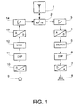
- FIG. 1 shows in a block diagram the function blocks of a transmit and a receiving branch of a mobile radio device, such as one Mobile phone conforms to the GSM standard.
- An antenna 1 is with a Antenna switch 2 coupled, the in a receive or transmit operation Receiving or transmitting branch connects to antenna 1.
- receive or transmitting branch connects to antenna 1.
- the analog radio signals arrive at an A / D converter via a receiving circuit 3 4.
- the generated digital signals are in a demodulator 5 demodulated and then fed to a digital signal processor (DSP) 6.
- DSP 6 digital signal processor
- the functions that are not shown in detail are successively Equalization, decryption, channel decoding and speech decoding performed.
- DSP digital signal processor
- the analog recorded by a microphone 9 Voice signals converted with an A / D converter 10 and then a DSP 11 fed.
- the DSP 11 performs the functions which are complementary to the reception mode Voice coding, channel coding and encryption through, all functions run from a single DSP.
- the binary coded data words are modulated in a modulator 12 GMSK and then in a D / A converter 13 in converted analog radio signals.
- a transmitter output stage 14 with a power amplifier generates the radio signal to be transmitted via antenna 1.
- the power amplifier 15 is connected to the antenna 1 via an impedance matching network 16 with a transformation factor T.
- the antenna 1 has an input resistance Z Ant , which has a value of, for example, 75 ⁇ .
- the input resistance Z Ant must be adapted to a required load Z PA of the power amplifier 15.
- the power amplifier 15 is supplied with an operating voltage U B by a battery, not shown. At the output, it delivers an output voltage U A , which is present at the respective load Z PA .
- the output power P PA of the power amplifier 15, which is effective on the real part of the load Z PA , ie is emitted as transmission power, is therefore always regulated to an exact value.
- P PA 1/2 ⁇ U A 2 / Z PA
- the output voltage U A thus also remains constant with a constant load Z PA .
- the load Z PA ie also the associated transformation factor T, is selected for a specific operating point of the output voltage U A.
- an efficiency ⁇ typically ⁇ > 40%
- ⁇ P PA / P total .
- This efficiency deteriorates as soon as the operating voltage U B compared to the set operating point, for example according to the typical one Discharge curve of the battery used is increased.
- the transformation factor T and thus the load Z PA of the power amplifier 15 can be switched between two values. This is described with reference to FIG. 3.
- the impedance matching network 16 is shown in more detail in FIG. 3.
- a first impedance transformer 17 designed as a ⁇ / 4 waveguide is connected on the one hand to the output of the power amplifier 15 and on the other hand to the input of the antenna 1.
- the ⁇ / 4 waveguide 17 can be implemented as a stripline, coaxial cable or through an LC network that simulates such a ⁇ / 4 waveguide.
- the impedance can be set using the geometric dimensions and the material constants.
- the waveguide can also be simulated by a line simulation with discrete components.
- the effective length of the waveguide can be adapted to the transmission frequency used.
- a second impedance transformer 18 is also realized by a ⁇ / 4 waveguide which is connected in parallel to the first ⁇ / 4 waveguide 17 on the power amplifier 15.
- the second ⁇ / 4 waveguide 18 is connected to a switch 19 which is connected to a ground connection in a first switch position and to the antenna 1 in a second switch position.
- the short circuit at the end in the first switch position is transformed by the ⁇ / 4 waveguide 18 to an open circuit at the beginning.
- the second ⁇ / 4 waveguide 18 is thus ineffective in this switch position.
- a new ⁇ / 4 waveguide is formed in the second switch position due to the ⁇ / 4 waveguides 17 and 18 connected in parallel.
- the transmitter output stage 14 is usually adapted to the antenna 1 in two transformation stages, of which the first stage is contained within the transmitter output stage 14.
- Z Ant 75 ⁇
- the first switch position results in a transformation to a value of 37.5 ⁇ .
- the load changes so that the output current I A of the power amplifier 15 is reduced at a constant output voltage U A. In this way, the current consumption of the transmitter output stage 14, for example when the operating voltage U B is increased by a battery, is reduced despite the constant regulated output power.
- a drop in efficiency from ⁇ > 40% to a value around 30% due to the mismatch can thus be prevented. Furthermore, only the ohmic load is changed by switching the load, while resonant circuits set to the transmission frequency are not detuned in their resonance frequency.
Landscapes
- Engineering & Computer Science (AREA)
- Computer Networks & Wireless Communication (AREA)
- Signal Processing (AREA)
- Transmitters (AREA)
- Mobile Radio Communication Systems (AREA)
- Transceivers (AREA)
Abstract
Description
- Figur 1:
- ein Blockdiagramm der Funktionsblöcke eines Mobilfunkgerätes,
- Figur 2:
- eine schematische Darstellung eines Teiles des Sendezweiges des Mobilfunkgerätes,
- Figur 3:
- ein detailliertere Darstellung eines Impedanzanpassungsnetzwerkes zwischen einer Senderendstufe und einer Antenne.
Claims (6)
- Mobilfunkgerät mit wenigstens einer Senderendstufe (14), mit wenigstens einer Antenne (1) und mit wenigstens einem zwischen Senderendstufe (14) und Antenne (1) angeordneten Impedanzanpassungsnetzwerk (16) mit einem Transformationsfaktor (T) zur Anpassung einer Senderlastimpedanz (ZPA) an eine Antenneneingangsimpedanz (ZAnt),
dadurch gekennzeichnet,
daß im Impedanzanpassungsnetzwerk (16) wenigstens zwei Impedanztransformatoren (17, 18) durch wahlweise Parallelschaltung zur Bildung von wenigstens zwei Transformationsfaktoren vorgesehen sind. - Mobilfunkgerät nach Anspruch 1,
dadurch gekennzeichnet,
daß wenigstens zwei λ/4-Wellenleiter (17, 18) zur Bildung der Impedanztransformatoren (17, 18) vorgesehen sind. - Mobilfunkgerät nach Anspruch 2,
dadurch gekennzeichnet,
daß im Impedanzanpassungsnetzwerk (16)ein erster λ/4-Wellenleiter (17) einerseits zur Kopplung mit dem Ausgang der Senderendstufe (15) und andererseits mit dem Eingang der Antenne (1) undein zweiter λ/4-Wellenleiter (18) einerseits zur Kopplung mit dem Ausgang der Senderendstufe (15) und andererseits mit wenigstens einem Schalter (19), der in einer ersten Schalterstellung die Verbindung mit einem Masseanschluß und in einer zweiten Schalterstellung mit dem Eingang der Antenne (1) herstellt, vorgesehen ist. - Mobilfunkgerät nach Anspruch 3,
dadurch gekennzeichnet,
daß ein mit PIN-Dioden realisierter Hochfrequenzschalter zur Bildung des Schalters (19) vorgesehen ist. - Mobilfunkgerät nach Anspruch 3,
dadurch gekennzeichnet,
daß ein bistabiles mechanisches Relais zur Bildung des Schalters (19) vorgesehen ist. - Sender mit wenigstens einer Senderendstufe (14), mit wenigstens einer Antenne (1) und mit wenigstens einem zwischen Senderendstufe (14) und Antenne (1) angeordneten Impedanzanpassungsnetzwerk (16) mit einem Transformationsfaktor (T) zur Anpassung einer Senderlastimpedanz (ZPA) an eine Antenneneingangsimpedanz (ZAnt),
dadurch gekennzeichnet,
daß im Impedanzanpassungsnetzwerk (16) wenigstens zwei Impedanztransformatoren (17, 18) durch wahlweise Parallelschaltung zur Bildung von wenigstens zwei Transformationsfaktoren vorgesehen sind.
Applications Claiming Priority (2)
| Application Number | Priority Date | Filing Date | Title |
|---|---|---|---|
| DE19757142 | 1997-12-20 | ||
| DE19757142A DE19757142A1 (de) | 1997-12-20 | 1997-12-20 | Mobilfunkgerät |
Publications (3)
| Publication Number | Publication Date |
|---|---|
| EP0924865A2 true EP0924865A2 (de) | 1999-06-23 |
| EP0924865A3 EP0924865A3 (de) | 2003-07-02 |
| EP0924865B1 EP0924865B1 (de) | 2005-06-08 |
Family
ID=7852923
Family Applications (1)
| Application Number | Title | Priority Date | Filing Date |
|---|---|---|---|
| EP98204255A Expired - Lifetime EP0924865B1 (de) | 1997-12-20 | 1998-12-15 | Antenneninpedanzanpassung eines Mobilfunkgerätes |
Country Status (6)
| Country | Link |
|---|---|
| US (1) | US6223022B1 (de) |
| EP (1) | EP0924865B1 (de) |
| JP (1) | JP4260955B2 (de) |
| KR (1) | KR100619605B1 (de) |
| CN (1) | CN1134903C (de) |
| DE (2) | DE19757142A1 (de) |
Families Citing this family (11)
| Publication number | Priority date | Publication date | Assignee | Title |
|---|---|---|---|---|
| US6556814B1 (en) * | 1999-07-22 | 2003-04-29 | Motorola, Inc. | Memory-based amplifier load adjust system |
| US6518856B1 (en) * | 1999-10-13 | 2003-02-11 | Signal Technology Corporation | RF power divider/combiner circuit |
| DE10119793A1 (de) * | 2001-04-23 | 2002-10-31 | Siemens Ag | Verfahren und Schaltungsanordnung zur Impedanzanpassung einer analogen Telekommunikationsverbindung |
| US6798314B2 (en) * | 2002-12-26 | 2004-09-28 | Intel Corporation | Transmit/receive combiner using shunt admittance elements for isolation |
| JP4175545B2 (ja) * | 2004-09-03 | 2008-11-05 | ソニー・エリクソン・モバイルコミュニケーションズ株式会社 | 無線通信端末 |
| JP4606843B2 (ja) * | 2004-11-01 | 2011-01-05 | 京セラ株式会社 | 無線通信モジュール、通信端末、およびインピーダンス整合方法 |
| EP1845627A4 (de) * | 2005-01-31 | 2014-07-30 | Panasonic Corp | Adaptive impedanzanpassungsfähige mobilfunk-vorrichtung |
| JP2009088770A (ja) * | 2007-09-28 | 2009-04-23 | Renesas Technology Corp | Rf増幅装置 |
| JP5381732B2 (ja) * | 2010-01-12 | 2014-01-08 | 三菱電機株式会社 | 高周波増幅器 |
| US10308383B2 (en) | 2014-07-21 | 2019-06-04 | Signode Industrial Group Llc | Electrically powered combination hand-held strapping tool |
| CN115622533B (zh) * | 2022-12-01 | 2023-03-21 | 深圳市恒运昌真空技术有限公司 | 一种阻抗匹配系统及方法 |
Family Cites Families (9)
| Publication number | Priority date | Publication date | Assignee | Title |
|---|---|---|---|---|
| FR2447111A1 (fr) * | 1978-07-11 | 1980-08-14 | Radiotechnique Compelec | Oscillateur hyperfrequence a large bande, a diode gunn, accorde par un grenat |
| JPS5851453B2 (ja) * | 1980-09-29 | 1983-11-16 | 日本電信電話株式会社 | 送信装置 |
| DE3811985A1 (de) * | 1988-04-11 | 1989-10-19 | Siemens Ag | Anordnung zur impedanztransformation |
| JP2830319B2 (ja) * | 1990-03-08 | 1998-12-02 | ソニー株式会社 | 送受信切り換え装置 |
| DE4222190A1 (de) * | 1992-07-07 | 1994-01-13 | Philips Patentverwaltung | Funkgerät mit einer Antennenumschaltvorrichtung |
| DE4441754A1 (de) * | 1993-12-21 | 1995-06-22 | Siemens Ag | Vorrichtung zur automatischen Impedanzanpassung einer HF-Sende- oder Empfangseinrichtung in einer Anlage zur Kernspintomographie und Verfahren zum Betrieb der Vorrichtung |
| KR970000654B1 (ko) * | 1994-09-27 | 1997-01-16 | 엘지전자 주식회사 | 셀룰라폰 안테나의 임피던스 조절장치 |
| SE509641C2 (sv) * | 1996-05-03 | 1999-02-15 | Allgon Ab | En antennanordning försedd med en matchningsanordning |
| US5654679A (en) * | 1996-06-13 | 1997-08-05 | Rf Power Products, Inc. | Apparatus for matching a variable load impedance with an RF power generator impedance |
-
1997
- 1997-12-20 DE DE19757142A patent/DE19757142A1/de not_active Ceased
-
1998
- 1998-12-15 EP EP98204255A patent/EP0924865B1/de not_active Expired - Lifetime
- 1998-12-15 DE DE59812852T patent/DE59812852D1/de not_active Expired - Lifetime
- 1998-12-16 CN CNB98123240XA patent/CN1134903C/zh not_active Expired - Fee Related
- 1998-12-18 KR KR1019980056303A patent/KR100619605B1/ko not_active Expired - Fee Related
- 1998-12-18 JP JP36143298A patent/JP4260955B2/ja not_active Expired - Fee Related
- 1998-12-21 US US09/217,434 patent/US6223022B1/en not_active Expired - Lifetime
Also Published As
| Publication number | Publication date |
|---|---|
| KR19990063213A (ko) | 1999-07-26 |
| EP0924865A3 (de) | 2003-07-02 |
| EP0924865B1 (de) | 2005-06-08 |
| CN1226106A (zh) | 1999-08-18 |
| KR100619605B1 (ko) | 2006-11-30 |
| JPH11251930A (ja) | 1999-09-17 |
| JP4260955B2 (ja) | 2009-04-30 |
| US6223022B1 (en) | 2001-04-24 |
| DE19757142A1 (de) | 1999-07-08 |
| DE59812852D1 (de) | 2005-07-14 |
| CN1134903C (zh) | 2004-01-14 |
Similar Documents
| Publication | Publication Date | Title |
|---|---|---|
| DE19823049C2 (de) | Leistungsverstärker-Ausgangsschaltung zur Unterdrückung von Oberschwingungen für eine Mobilfunkeinheit mit Doppelbandbetrieb und Verfahren zum Betreiben derselben | |
| DE60116676T2 (de) | Mehrband-Transformationsstufe für eine Mehrband-HF-Umschaltvorrichtung | |
| DE69427245T2 (de) | Antennenweiche und Sende-Empfangsgerät mit Anwendung desselben | |
| DE69715717T2 (de) | Zweiband-Oszillatorschaltung | |
| DE69929968T2 (de) | Antennenschalter | |
| DE60225032T2 (de) | Vorrichtung zur impedanzanpassung in einem verstärker unter verwendung von konzentrierter und verteilter induktanz | |
| DE10150159B4 (de) | Impedanzanpassungsschaltung für einen Mehrband-Leisungsverstärker | |
| DE102013217545B4 (de) | System und verfahren für das senden eines hochfrequenzsignals mittels einer lautsprecherspule | |
| EP0578324B1 (de) | Funkgerät mit einer Antennenumschaltvorrichtung | |
| EP0927438B1 (de) | Antennenanordnung mit kapazitiv abstimmbarem rahmen und funkrufempfänger | |
| EP0924865B1 (de) | Antenneninpedanzanpassung eines Mobilfunkgerätes | |
| WO2000018026A1 (de) | Mehrband-antennenschalter | |
| DE19853484A1 (de) | Hochfrequente Schalteinrichtung | |
| EP0862279A2 (de) | Sende-Empfangs-Umschalteanordnung | |
| DE2757627A1 (de) | Mikrowellenphasenschieber mit einer einrichtung zur energieein- oder auskopplung | |
| CH684722A5 (de) | Schaltungsanordnung zur Ankopplung einer Sendeeinheit an eine Uebertragungsleitung. | |
| DE4342249C2 (de) | Antennenschalter und Verfahren zum Verbinden oder Entkoppeln eines Empfängerschaltkreises mit einer Antenne | |
| WO2000046934A1 (de) | Sender-/empfänger-einheit für eine erste und eine zweite sende-/empfangsfrequenz | |
| DE19930195C2 (de) | Schaltung zum Verstärken eines Hochfrequenzsignals aus zumindest zwei Hochfrequenzbereichen, 2-Band-Empfänger mit der Schaltung, 2-Band-Mobilfunkvorrichtung mit dem Empfänger und Verwendung einer Serienschaltung aus einem kapazitiven Element und einer Hochfrequenzleitung in einer Verstärkerschaltung | |
| DE69904560T2 (de) | Sender | |
| DE2554828C3 (de) | Aktive Empfangsantenne mit gegengekoppeltem Verstärker | |
| DE2065525C3 (de) | Einrichtung zur Einspeisung einer hochfrequenten über ein Parallelkreisfilter ankommenden Signalenergie in eine durchgehende Leitung | |
| DE19532470B4 (de) | Selektiver Multikoppler | |
| EP0399202B1 (de) | Hochfrequenz-Richtkopplerabzweiger | |
| DE4105146C2 (de) | Hochfrequenz-Entkoppelungsschaltung |
Legal Events
| Date | Code | Title | Description |
|---|---|---|---|
| PUAI | Public reference made under article 153(3) epc to a published international application that has entered the european phase |
Free format text: ORIGINAL CODE: 0009012 |
|
| AK | Designated contracting states |
Kind code of ref document: A2 Designated state(s): AT BE CH CY DE DK ES FI FR GB GR IE IT LI LU MC NL PT SE |
|
| AX | Request for extension of the european patent |
Free format text: AL;LT;LV;MK;RO;SI |
|
| RAP3 | Party data changed (applicant data changed or rights of an application transferred) |
Owner name: KONINKLIJKE PHILIPS ELECTRONICS N.V. Owner name: PHILIPS CORPORATE INTELLECTUAL PROPERTY GMBH |
|
| RAP1 | Party data changed (applicant data changed or rights of an application transferred) |
Owner name: KONINKLIJKE PHILIPS ELECTRONICS N.V. Owner name: PHILIPS CORPORATE INTELLECTUAL PROPERTY GMBH |
|
| RAP1 | Party data changed (applicant data changed or rights of an application transferred) |
Owner name: KONINKLIJKE PHILIPS ELECTRONICS N.V. Owner name: PHILIPS INTELLECTUAL PROPERTY & STANDARDS GMBH |
|
| PUAL | Search report despatched |
Free format text: ORIGINAL CODE: 0009013 |
|
| AK | Designated contracting states |
Designated state(s): AT BE CH CY DE DK ES FI FR GB GR IE IT LI LU MC NL PT SE |
|
| AX | Request for extension of the european patent |
Extension state: AL LT LV MK RO SI |
|
| 17P | Request for examination filed |
Effective date: 20040102 |
|
| AKX | Designation fees paid |
Designated state(s): DE FR GB |
|
| GRAP | Despatch of communication of intention to grant a patent |
Free format text: ORIGINAL CODE: EPIDOSNIGR1 |
|
| GRAS | Grant fee paid |
Free format text: ORIGINAL CODE: EPIDOSNIGR3 |
|
| GRAA | (expected) grant |
Free format text: ORIGINAL CODE: 0009210 |
|
| AK | Designated contracting states |
Kind code of ref document: B1 Designated state(s): DE FR GB |
|
| REG | Reference to a national code |
Ref country code: GB Ref legal event code: FG4D Free format text: NOT ENGLISH |
|
| REF | Corresponds to: |
Ref document number: 59812852 Country of ref document: DE Date of ref document: 20050714 Kind code of ref document: P |
|
| GBT | Gb: translation of ep patent filed (gb section 77(6)(a)/1977) |
Effective date: 20050902 |
|
| ET | Fr: translation filed | ||
| PLBE | No opposition filed within time limit |
Free format text: ORIGINAL CODE: 0009261 |
|
| STAA | Information on the status of an ep patent application or granted ep patent |
Free format text: STATUS: NO OPPOSITION FILED WITHIN TIME LIMIT |
|
| 26N | No opposition filed |
Effective date: 20060309 |
|
| REG | Reference to a national code |
Ref country code: GB Ref legal event code: 732E |
|
| REG | Reference to a national code |
Ref country code: GB Ref legal event code: 732E |
|
| REG | Reference to a national code |
Ref country code: FR Ref legal event code: TP |
|
| REG | Reference to a national code |
Ref country code: FR Ref legal event code: GC |
|
| REG | Reference to a national code |
Ref country code: GB Ref legal event code: 732E Free format text: REGISTERED BETWEEN 20090618 AND 20090624 |
|
| REG | Reference to a national code |
Ref country code: FR Ref legal event code: GC |
|
| PGFP | Annual fee paid to national office [announced via postgrant information from national office to epo] |
Ref country code: FR Payment date: 20091221 Year of fee payment: 12 |
|
| PGFP | Annual fee paid to national office [announced via postgrant information from national office to epo] |
Ref country code: DE Payment date: 20091222 Year of fee payment: 12 |
|
| REG | Reference to a national code |
Ref country code: GB Ref legal event code: 732E Free format text: REGISTERED BETWEEN 20101007 AND 20101013 |
|
| PGFP | Annual fee paid to national office [announced via postgrant information from national office to epo] |
Ref country code: GB Payment date: 20101215 Year of fee payment: 13 |
|
| REG | Reference to a national code |
Ref country code: FR Ref legal event code: GC |
|
| REG | Reference to a national code |
Ref country code: FR Ref legal event code: ST Effective date: 20110831 |
|
| PG25 | Lapsed in a contracting state [announced via postgrant information from national office to epo] |
Ref country code: FR Free format text: LAPSE BECAUSE OF NON-PAYMENT OF DUE FEES Effective date: 20110103 |
|
| REG | Reference to a national code |
Ref country code: GB Ref legal event code: 732E Free format text: REGISTERED BETWEEN 20111013 AND 20111019 |
|
| REG | Reference to a national code |
Ref country code: DE Ref legal event code: R119 Ref document number: 59812852 Country of ref document: DE Effective date: 20110701 |
|
| PG25 | Lapsed in a contracting state [announced via postgrant information from national office to epo] |
Ref country code: DE Free format text: LAPSE BECAUSE OF NON-PAYMENT OF DUE FEES Effective date: 20110701 |
|
| REG | Reference to a national code |
Ref country code: FR Ref legal event code: AU Effective date: 20120126 |
|
| REG | Reference to a national code |
Ref country code: GB Ref legal event code: 732E Free format text: REGISTERED BETWEEN 20120315 AND 20120321 |
|
| REG | Reference to a national code |
Ref country code: GB Ref legal event code: 732E Free format text: REGISTERED BETWEEN 20120705 AND 20120711 |
|
| REG | Reference to a national code |
Ref country code: GB Ref legal event code: 732E Free format text: REGISTERED BETWEEN 20120927 AND 20121003 |
|
| GBPC | Gb: european patent ceased through non-payment of renewal fee |
Effective date: 20121215 |
|
| PG25 | Lapsed in a contracting state [announced via postgrant information from national office to epo] |
Ref country code: GB Free format text: LAPSE BECAUSE OF NON-PAYMENT OF DUE FEES Effective date: 20121215 |