EP0925604B1 - Methode zur herstellung einer elektronischen schaltung, wobei eine leitetende schicht auf einer isolierenden schicht hergestellt wird und daraus ein leitungsmuster gemacht wird - Google Patents
Methode zur herstellung einer elektronischen schaltung, wobei eine leitetende schicht auf einer isolierenden schicht hergestellt wird und daraus ein leitungsmuster gemacht wird Download PDFInfo
- Publication number
- EP0925604B1 EP0925604B1 EP98910928A EP98910928A EP0925604B1 EP 0925604 B1 EP0925604 B1 EP 0925604B1 EP 98910928 A EP98910928 A EP 98910928A EP 98910928 A EP98910928 A EP 98910928A EP 0925604 B1 EP0925604 B1 EP 0925604B1
- Authority
- EP
- European Patent Office
- Prior art keywords
- layer
- windows
- silicon
- dielectric layer
- conductive layer
- Prior art date
- Legal status (The legal status is an assumption and is not a legal conclusion. Google has not performed a legal analysis and makes no representation as to the accuracy of the status listed.)
- Expired - Lifetime
Links
Images

Classifications
-
- H—ELECTRICITY
- H10—SEMICONDUCTOR DEVICES; ELECTRIC SOLID-STATE DEVICES NOT OTHERWISE PROVIDED FOR
- H10D—INORGANIC ELECTRIC SEMICONDUCTOR DEVICES
- H10D64/00—Electrodes of devices having potential barriers
- H10D64/01—Manufacture or treatment
- H10D64/011—Manufacture or treatment of electrodes ohmically coupled to a semiconductor
-
- H—ELECTRICITY
- H10—SEMICONDUCTOR DEVICES; ELECTRIC SOLID-STATE DEVICES NOT OTHERWISE PROVIDED FOR
- H10P—GENERIC PROCESSES OR APPARATUS FOR THE MANUFACTURE OR TREATMENT OF DEVICES COVERED BY CLASS H10
- H10P50/00—Etching of wafers, substrates or parts of devices
- H10P50/71—Etching of wafers, substrates or parts of devices using masks for conductive or resistive materials
Definitions
- the invention relates to a method of manufacturing an electronic device.
- the invention is of particular importance for monolithically integrated circuits.
- the invention may also be of importance for other devices in which electrical conductors are provided at very small distances from one another, as will become clear from the description, such as, for example, PCBs, or control matrices for LCDs.
- Auxiliary windows are provided in the oxide layer at the areas of the gaps between the gates to be formed for this purpose, the dimensions of the auxiliary windows being greater than those of the gaps to be eventually obtained
- the oxide layer is etched throughout its entire thickness, so that the WSi layer lies exposed in the auxiliary windows.
- the mask windows of reduced dimensions are obtained through the application of spacers on the side walls of the auxiliary windows.
- the silicon oxide layer is etched down to the gates to be formed. This may give rise to problems if the etching selectivity between silicon oxide and the conductor material is not sufficiently great, because in that case the gate material will also be attacked.
- the material of the gates should not or at least substantially not be made locally thinner owing to the etching of the silicon oxide layer, especially in cases where the conductor layer is very thin, for example comprises a layer of 60 nm thick polycrystalline silicon (poly) in view of the envisaged photosensitivity of the CCD imager.
- the invention accordingly has for its object inter alia to modify a method of the kind mentioned in the opening paragraph in such a manner that the conductor material of the gates is not or substantially not attacked by the etchant for the silicon oxide layer.
- the invention is defined by claim 1.
- the dependent claims define advantageous embodiments.
- the fact that the spacers are provided on the side walls of the auxiliary windows in a stage in which the conductive layer is still entirely covered by the dielectric layer, in accordance with the invention, means that at most those portions of the conductive layer which are situated at the areas of the gaps to be formed, i.e. which will be removed anyway, are exposed to the etching treatment the moment the etching has progressed so far that the conductive layer is reached.
- a layer of a suitable metal or of a conductive metal compound, for example a metal silicide, may be used as the conductive layer.
- the conductive layer is provided in the form of a layer comprising silicon.
- the electrically insulating substrate is formed by an electrically insulating layer which is provided on a surface of a silicon body.
- the electrically insulating layer is provided as a dual layer comprising a sub-layer formed by a silicon nitride layer and a sub-layer of silicon oxide which is separated from the conductive layer by the nitride layer.
- nitride which forms an oxidation mask, renders it possible to carry out an oxidation step in the gaps between the conductor tracks, whereby undesirable short-circuits between the conductor tracks are prevented.
- a corresponding pattern of openings may be advantageously provided in the conductive layer by etching, whereupon the exposed side walls of the conductor tracks can be oxidized by means of said oxidation step.
- a preferred embodiment, in which a further reduction of the gaps between the conductor tracks can be obtained, is characterized in that the silicon oxide layer is provided to a thickness which is greater than the thickness of the silicon nitride layer which forms said mask, whereupon said silicon oxide layer is provided with auxiliary windows which extend over only part of the silicon oxide layer at the areas of the windows to be formed, whereupon the additional layer also comprising silicon oxide is provided.
- Such a method is particularly advantageous for conductive layers having a small or very small thickness, for example a thickness of at most 0.1 ⁇ m.
- the oxidation is carried out in an oxidizing environment containing water vapor.
- the drawing is diagrammatic and not true to scale.
- the invention is explained with reference to a charge coupled device, in particular an imaging device, in which it is of major importance that the electrodes should be at very small distances from one another. It is usual to provide the electrodes in a multilayer wiring in which adjoining electrodes overlap. Major advantages are obtained when the electrodes can be formed in a single poly layer, whereby process steps can be dispensed with and in addition a more planar structure can be obtained. It will become clear from the ensuing description that the invention has a much wider field of application than CCDs alone and, in general, may be applied wherever electrodes are to be provided at very small distances from one another on an electrically insulating substrate.
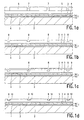
- the insulating substrate is formed by a gate dielectric layer 1 provided on the surface of a silicon body 2 (Fig. la).
- the conductivity type and the doping concentration in the semiconductor body are such that CCD operation is possible in the body 2.
- the dielectric layer 1 may comprise a single layer of, for example, silicon oxide, but in the present example comprises a dual layer with a layer 1a of silicon oxide and a layer 1b of silicon nitride. The presence of the nitride layer 1b renders it possible inter alia to carry out oxidation steps without appreciably changing the gate dielectric 1.
- a doped polycrystalline silicon layer 3 (poly) in which the gates or electrodes of the charge coupled device are to be defined is provided on the dielectric layer 1.
- the layer 3 is made very thin, i.e. thinner than approximately 0.1 ⁇ m.
- the thickness of the poly layer 3 is approximately 60 nm in the present example.
- a second silicon nitride layer, the layer 4 is provided on the poly layer 3 so as to form an oxidation mask for the poly layer 3.
- a comparatively thick ( ⁇ 0,5 ⁇ m) oxide layer 5 is deposited on the nitride layer 4.
- a photoresist layer is provided thereon, and an etching mask 6 is formed in this photoresist in a usual manner, with openings 7 at the areas of the gaps to be formed between the gates.
- the width of the openings 7 is, for example, 0.5 ⁇ m.
- Fig. la shows this stage in the process.
- the pattern of openings 7 in the photoresist layer 6 is transferred to the dielectric layer 4, 5 by means of anisotropic etching.
- the openings can be provided right across the thickness of the oxide layer 5 down to the nitride layer.
- the layer 5 is not etched throughout its entire thickness, but only through part of its thickness, for example through half or approximately half the layer 5 as shown in Fig. 1b .
- This Figure shows the device after the photoresist layer 6 has been removed subsequent to the etching of the oxide 5.
- the windows 8 in the oxide layer 5 have dimensions which correspond to those of the openings 7 in the mask 6 and are considerably greater, as will become apparent below, than those of the gaps to be formed in the conductive layer 3.
- an additional oxide layer 9 is formed with a thickness of, for example, 0.25 ⁇ m, the pattern of windows 8 being present also in this additional layer.
- the layer 9 is subsequently removed again by means of anisotropic etching-back, such that, at the moment when the horizontal portions of the layer 9 have been removed, only portions 10 of the additional layer, referred to as spacers for short, remain on the side walls of the auxiliary windows 8 ( Fig. 1d ), strongly reducing the dimensions of the auxiliary windows 8.
- the etching treatment is continued (without mask) until the windows 11 ( Fig. 1e ) are obtained, which windows extend straight across the thickness of the remaining oxide layer 5 down to the nitride layer 4.
- the windows 11 have a tapering shape in downward direction, so that the width at the bottom of the windows 11 is considerably smaller than that at the top and is no more than approximately 0.2 ⁇ m.
- the etching treatment may be simply stopped the moment the poly layer 3 is reached.
- Fig. 1f shows the device in this stage of the process.
- the silicon oxide layer 5 can then be removed (Fig. lg).
- the silicon nitride layer 4, provided with the very narrow windows 11, is used as a mask in the subsequent oxidation step in which the silicon of the poly layer 3 lying exposed in the windows 11 is converted into silicon oxide 12 by means of oxidation.
- the oxidized portions 12 extend through the entire thickness of the conductive layer 3 and define gates 13 in this layer which are mutually separated by the oxidized portions 12 ( Fig. 1h ).
- the oxidation step can be carried out such that short-circuits between adjoining gates 13 is prevented. To make the gaps between the gates 13 as small as possible, moreover, the oxidation is carried out in an oxidizing environment comprising water vapor.
- the poly layer 3 can be oxidized through its entire thickness in a comparatively short period at a temperature of 1000 °C.
- the width of the inter-electrode gaps was 0.2-0.25 ⁇ m, which is sufficiently small for achieving a satisfactory operation of the charge coupled device.
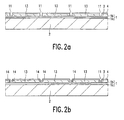
- Fig. 2 shows a modification of the manufacturing process described above, starting with the situation of Fig. 1g , where the nitride layer 4 is provided with the narrow windows 11. Instead of an oxidation step, the poly layer 3 is now first subjected to an etching treatment whereby the openings 11 are formed also in the poly layer 3 right through the thickness of the poly layer.
- the electrodes 13 have already been formed in the poly layer 3 through the openings 11 at this stage. Then, see Fig. 2b , a light oxidation step is carried out. Any residues of conductor material between the gates 13 are converted into electrically insulating oxide by this oxidation step, so that short-circuits between gates are prevented. In addition, the lateral sides of the gates are covered with a thin oxide layer 14 during this oxidation step.
- the width of the inter-electrode gaps is determined by the width of the windows 11 augmented by the widths of the oxidized edges of the electrodes. The total gap width may accordingly be slightly greater than in the preceding embodiment.
- this modification of the method is also suitable for use with greater thicknesses of the poly layer 3.
- the nitride-poly-nitride layer structure as used in the examples may also be used for manufacturing so-called MNOS memory elements, the letters M, N, O, and S denoting metal for the gate electrode (poly in the present case), nitride, oxide, and semiconductor material, respectively.
- MNOS memory elements the letters M, N, O, and S denoting metal for the gate electrode (poly in the present case), nitride, oxide, and semiconductor material, respectively.
- information is stored in the form of electric charge at the boundary surface between the nitride and the oxide.
- the nitride layer 1b is not used.
- the invention may also be applied outside the field of integrated circuits, for example, if conductors are to be provided close together on a glass substrate or on a PCB.
Landscapes
- Internal Circuitry In Semiconductor Integrated Circuit Devices (AREA)
- Solid State Image Pick-Up Elements (AREA)
- Wire Bonding (AREA)
Claims (10)
- Ein Verfahren zur Herstellung eines elektronischen Bauelementes, umfassend die folgenden Schritte:Bereitstellen einer leitenden Schicht (3) auf einem elektrisch isolierenden Substrat (1, 2),Bereitstellen einer Dielektrikumschicht (5) mit einer Dicke aufbesagter leitender Schicht (3),Bilden einer Photoresistschicht (6) auf besagter Dielektrikumschicht (5),Versehen besagter Photoresistschicht (6) mit einem Muster durch Lithographie, um in besagter Photoresistschicht ein Muster aus Fenstern (7) zu bilden, das einem Muster entspricht, das aus besagter leitender Schicht (3) zu bilden ist,Übertragen besagten Musters aus Fenstern (7) auf besagte Dielektrikumschicht (5) mittels anisotropischen Ätzens durch einen Teil besagter Dicke hindurch, um eine gemusterte Dielektrikumschicht (5) mit Vertiefungen (8) zu bilden,Entfernen der gemusterten Photoresistschicht (6),Bilden einer zusätzlichen Dielektrikumschicht (9) aufbesagtem gemusterten Dielektrikum (4, 5),anisotropisches Ätzen besagter zusätzlicher Dielektrikumschicht (9), so dass in dem Moment, wo horizontale Abschnitte besagter zusätzlicher Dielektrikumschicht (9) entfernt werden, Abstandshalter (10) besagter zusätzlicher Dielektrikumschicht (9) auf den Seitenwänden besagter Vertiefungen (8) verbleiben, und Fortsetzen besagten anisotropischen Ätzens, bis besagte leitende Schicht (3) erreicht ist, wodurch in besagter Dielektrikumschicht (5) konisch zulaufende Fenster (11) gebildet werden, die an der offen liegenden leitenden Schicht geringere Abmessungen haben als an den oberen Enden besagter konisch zulaufender Fenster, undVersehen besagter leitender Schicht mit einem Muster unter Verwendung besagter Dielektrikumschicht (5) mit besagten konisch zulaufenden Fenstern als Maske, um ein Leitermuster zu bilden.
- Ein Verfahren nach Anspruch 1, wobei besagtes elektrisch isolierendes Substrat aus einer elektrisch isolierenden Schicht (1) auf einer Oberfläche eines Siliziumkörpers (2) gebildet wird und besagte leitende Schicht (3) auf besagter elektrisch isolierender Schicht (1) gebildet wird.
- Ein Verfahren nach Anspruch 1 oder 2, wobei besagte leitende Schicht aus Silizium ist.
- Ein Verfahren nach Anspruch 3, wobei besagte Dielektrikumschicht (5) als Doppelschicht, umfassend eine Siliziumnitridschicht (4) und eine Siliziumoxidschicht (5), bereitgestellt wird, die durch besagte Siliziumnitridschicht von besagter leitender Schicht getrennt ist.
- Ein Verfahren nach Anspruch 4, wobei die Siliziumoxidschicht (5) in einer Dicke bereitgestellt wird, die größer als die Dicke der Siliziumnitridschicht ist, die besagte Maske bildet, und wobei das Übertragen besagten Musters aus Fenstern dergestalt ist, dass das anisotropische Ätzen durch einen Teil der Dicke besagter Siliziumoxidschicht hindurch erfolgt und besagte zusätzliche Dielektrikumschicht Siliziumoxid umfasst.
- Ein Verfahren nach Anspruch 5, wobei das Versehen der leitenden Schicht mit einem Muster durch Oxidation des offen liegenden Siliziums durch die gesamte Dicke besagter leitender Schicht hindurch realisiert wird.
- Ein Verfahren nach Anspruch 6, wobei besagte Oxidation in einer oxidierenden Umgebung, die Wasserdampf enthält, durchgeführt wird.
- Ein Verfahren nach einem der Ansprüche 3 bis 7, wobei besagte elektrisch isolierende Schicht (1) eine erste Siliziumoxidschicht (1a), die aufbesagtem Siliziumkörper bereitgestellt ist, und eine erste Siliziumnitridschicht (1b), die auf besagter erster Siliziumoxidschicht bereitgestellt ist, umfasst und besagte leitende Schicht (3) auf besagter erster Siliziumnitridschicht (1b) bereitgestellt ist.
- Ein Verfahren nach Anspruch 8, wobei ein Leitermuster in Form einer Anzahl von nebeneinander angeordneten Leiterbahnen bereitgestellt wird, die sich parallel zueinander über besagte elektrisch isolierende Schicht (1) erstrecken und die in Zusammenwirkung mit dem darunter liegenden Siliziumkörper Gate-Elektroden eines ladungsgekoppelten Bauelementes bilden.
- Ein Verfahren nach einem der Ansprüche 3 bis 9, wobei besagte leitende Schicht aus polykristallinem Silizium ist und eine Dicke von höchstens 0,1 µm hat.
Priority Applications (1)
| Application Number | Priority Date | Filing Date | Title |
|---|---|---|---|
| EP98910928A EP0925604B1 (de) | 1997-05-29 | 1998-04-09 | Methode zur herstellung einer elektronischen schaltung, wobei eine leitetende schicht auf einer isolierenden schicht hergestellt wird und daraus ein leitungsmuster gemacht wird |
Applications Claiming Priority (4)
| Application Number | Priority Date | Filing Date | Title |
|---|---|---|---|
| EP97201585 | 1997-05-29 | ||
| EP97201585 | 1997-05-29 | ||
| PCT/IB1998/000541 WO1998054755A2 (en) | 1997-05-29 | 1998-04-09 | A method of manufacturing an electronic device whereby a conductive layer is provided on an electrically insulating substrate, from which layer a conductor pattern is formed |
| EP98910928A EP0925604B1 (de) | 1997-05-29 | 1998-04-09 | Methode zur herstellung einer elektronischen schaltung, wobei eine leitetende schicht auf einer isolierenden schicht hergestellt wird und daraus ein leitungsmuster gemacht wird |
Publications (2)
| Publication Number | Publication Date |
|---|---|
| EP0925604A2 EP0925604A2 (de) | 1999-06-30 |
| EP0925604B1 true EP0925604B1 (de) | 2008-07-09 |
Family
ID=8228365
Family Applications (1)
| Application Number | Title | Priority Date | Filing Date |
|---|---|---|---|
| EP98910928A Expired - Lifetime EP0925604B1 (de) | 1997-05-29 | 1998-04-09 | Methode zur herstellung einer elektronischen schaltung, wobei eine leitetende schicht auf einer isolierenden schicht hergestellt wird und daraus ein leitungsmuster gemacht wird |
Country Status (6)
| Country | Link |
|---|---|
| US (1) | US6054336A (de) |
| EP (1) | EP0925604B1 (de) |
| JP (1) | JP2000515330A (de) |
| KR (1) | KR100519834B1 (de) |
| DE (1) | DE69839693D1 (de) |
| WO (1) | WO1998054755A2 (de) |
Families Citing this family (3)
| Publication number | Priority date | Publication date | Assignee | Title |
|---|---|---|---|---|
| US6525356B1 (en) * | 1998-12-15 | 2003-02-25 | Nec Corporation | Solid imaging device |
| EP1386353A2 (de) * | 2001-05-01 | 2004-02-04 | Koninklijke Philips Electronics N.V. | Verfahren zur herstellung von verbindungsleitungen in einer halbleitervorrichtung |
| JP4491375B2 (ja) * | 2005-04-26 | 2010-06-30 | 日本電気株式会社 | 液晶表示装置の製造方法 |
Family Cites Families (10)
| Publication number | Priority date | Publication date | Assignee | Title |
|---|---|---|---|---|
| NL9100094A (nl) * | 1991-01-21 | 1992-08-17 | Koninkl Philips Electronics Nv | Halfgeleiderinrichting en werkwijze ter vervaardiging van een dergelijke halfgeleiderinrichting. |
| DE59409300D1 (de) * | 1993-06-23 | 2000-05-31 | Siemens Ag | Verfahren zur Herstellung von einem Isolationsgraben in einem Substrat für Smart-Power-Technologien |
| JP3560990B2 (ja) * | 1993-06-30 | 2004-09-02 | 株式会社東芝 | 固体撮像装置 |
| US5572040A (en) * | 1993-07-12 | 1996-11-05 | Peregrine Semiconductor Corporation | High-frequency wireless communication system on a single ultrathin silicon on sapphire chip |
| JPH08204173A (ja) * | 1995-01-25 | 1996-08-09 | Sony Corp | 電荷転送装置の製造方法 |
| US5589407A (en) * | 1995-09-06 | 1996-12-31 | Implanted Material Technology, Inc. | Method of treating silicon to obtain thin, buried insulating layer |
| US5573961A (en) * | 1995-11-09 | 1996-11-12 | Taiwan Semiconductor Manufacturing Company Ltd. | Method of making a body contact for a MOSFET device fabricated in an SOI layer |
| JPH09172061A (ja) * | 1995-12-18 | 1997-06-30 | Fuji Electric Co Ltd | 半導体装置の製造方法 |
| US5914280A (en) * | 1996-12-23 | 1999-06-22 | Harris Corporation | Deep trench etch on bonded silicon wafer |
| US5811315A (en) * | 1997-03-13 | 1998-09-22 | National Semiconductor Corporation | Method of forming and planarizing deep isolation trenches in a silicon-on-insulator (SOI) structure |
-
1998
- 1998-04-09 KR KR10-1999-7000651A patent/KR100519834B1/ko not_active Expired - Lifetime
- 1998-04-09 JP JP10529397A patent/JP2000515330A/ja not_active Ceased
- 1998-04-09 EP EP98910928A patent/EP0925604B1/de not_active Expired - Lifetime
- 1998-04-09 WO PCT/IB1998/000541 patent/WO1998054755A2/en not_active Ceased
- 1998-04-09 DE DE69839693T patent/DE69839693D1/de not_active Expired - Lifetime
- 1998-05-26 US US09/085,085 patent/US6054336A/en not_active Expired - Lifetime
Also Published As
| Publication number | Publication date |
|---|---|
| EP0925604A2 (de) | 1999-06-30 |
| WO1998054755A2 (en) | 1998-12-03 |
| KR100519834B1 (ko) | 2005-10-06 |
| JP2000515330A (ja) | 2000-11-14 |
| WO1998054755A3 (en) | 1999-03-04 |
| KR20000029590A (ko) | 2000-05-25 |
| DE69839693D1 (de) | 2008-08-21 |
| US6054336A (en) | 2000-04-25 |
Similar Documents
| Publication | Publication Date | Title |
|---|---|---|
| US5444021A (en) | Method for making a contact hole of a semiconductor device | |
| JP3560990B2 (ja) | 固体撮像装置 | |
| US5872035A (en) | Method of forming a floating gate in a flash memory device | |
| US5989987A (en) | Method of forming a self-aligned contact in semiconductor fabrications | |
| US5600170A (en) | Interconnection structure of semiconductor device | |
| JPH06318562A (ja) | 半導体装置およびその製造方法 | |
| US6093627A (en) | Self-aligned contact process using silicon spacers | |
| KR100238865B1 (ko) | 불휘발성 반도체 메모리 장치의 메모리 셀의 제조방법 | |
| EP0925604B1 (de) | Methode zur herstellung einer elektronischen schaltung, wobei eine leitetende schicht auf einer isolierenden schicht hergestellt wird und daraus ein leitungsmuster gemacht wird | |
| US6077763A (en) | Process for fabricating a self-aligned contact | |
| US6995349B2 (en) | Solid-state image pickup device and method for manufacturing the same | |
| KR100258880B1 (ko) | 반도체 소자의 제조방법 | |
| JP2623019B2 (ja) | 半導体装置 | |
| US5925919A (en) | CMOS Semiconductor structure and process for producing the same | |
| KR100272558B1 (ko) | 고체 촬상 소자의 제조방법 | |
| JP2828089B2 (ja) | 半導体装置の製造方法 | |
| KR100213203B1 (ko) | 콘택홀을 가지는 반도체 장치 및 그의 형성방법 | |
| KR100518527B1 (ko) | 저저항의 게이트 전극을 갖는 반도체 소자의 제조방법 | |
| US20020061658A1 (en) | Method of forming a semiconductor structure | |
| KR100280521B1 (ko) | 반도체소자 및 그 제조방법 | |
| JP3239422B2 (ja) | 接続構造の形成方法及び該接続構造の形成方法を用いた電子材料の形成方法 | |
| KR101132722B1 (ko) | 반도체 소자의 게이트 전극 형성방법 | |
| KR100593156B1 (ko) | 시모스 이미지센서의 제조방법 | |
| KR20000046947A (ko) | 아날로그 반도체소자의 제조방법 | |
| JPH1117165A (ja) | 半導体装置の積層ゲート構造 |
Legal Events
| Date | Code | Title | Description |
|---|---|---|---|
| PUAI | Public reference made under article 153(3) epc to a published international application that has entered the european phase |
Free format text: ORIGINAL CODE: 0009012 |
|
| 17P | Request for examination filed |
Effective date: 19990301 |
|
| AK | Designated contracting states |
Kind code of ref document: A2 Designated state(s): DE FR GB IT NL |
|
| 17Q | First examination report despatched |
Effective date: 20050502 |
|
| 17Q | First examination report despatched |
Effective date: 20050502 |
|
| RAP1 | Party data changed (applicant data changed or rights of an application transferred) |
Owner name: NXP B.V. |
|
| GRAP | Despatch of communication of intention to grant a patent |
Free format text: ORIGINAL CODE: EPIDOSNIGR1 |
|
| GRAS | Grant fee paid |
Free format text: ORIGINAL CODE: EPIDOSNIGR3 |
|
| GRAA | (expected) grant |
Free format text: ORIGINAL CODE: 0009210 |
|
| AK | Designated contracting states |
Kind code of ref document: B1 Designated state(s): DE FR GB IT NL |
|
| REG | Reference to a national code |
Ref country code: GB Ref legal event code: FG4D |
|
| REF | Corresponds to: |
Ref document number: 69839693 Country of ref document: DE Date of ref document: 20080821 Kind code of ref document: P |
|
| NLV1 | Nl: lapsed or annulled due to failure to fulfill the requirements of art. 29p and 29m of the patents act | ||
| PG25 | Lapsed in a contracting state [announced via postgrant information from national office to epo] |
Ref country code: NL Free format text: LAPSE BECAUSE OF FAILURE TO SUBMIT A TRANSLATION OF THE DESCRIPTION OR TO PAY THE FEE WITHIN THE PRESCRIBED TIME-LIMIT Effective date: 20080709 |
|
| PLBE | No opposition filed within time limit |
Free format text: ORIGINAL CODE: 0009261 |
|
| STAA | Information on the status of an ep patent application or granted ep patent |
Free format text: STATUS: NO OPPOSITION FILED WITHIN TIME LIMIT |
|
| 26N | No opposition filed |
Effective date: 20090414 |
|
| PG25 | Lapsed in a contracting state [announced via postgrant information from national office to epo] |
Ref country code: IT Free format text: LAPSE BECAUSE OF FAILURE TO SUBMIT A TRANSLATION OF THE DESCRIPTION OR TO PAY THE FEE WITHIN THE PRESCRIBED TIME-LIMIT Effective date: 20080709 |
|
| PGFP | Annual fee paid to national office [announced via postgrant information from national office to epo] |
Ref country code: FR Payment date: 20100521 Year of fee payment: 13 |
|
| REG | Reference to a national code |
Ref country code: FR Ref legal event code: ST Effective date: 20111230 |
|
| PG25 | Lapsed in a contracting state [announced via postgrant information from national office to epo] |
Ref country code: FR Free format text: LAPSE BECAUSE OF NON-PAYMENT OF DUE FEES Effective date: 20110502 |
|
| REG | Reference to a national code |
Ref country code: GB Ref legal event code: 732E Free format text: REGISTERED BETWEEN 20120315 AND 20120321 |
|
| REG | Reference to a national code |
Ref country code: DE Ref legal event code: R082 Ref document number: 69839693 Country of ref document: DE Representative=s name: BOSCH JEHLE PATENTANWALTSGESELLSCHAFT MBH, DE |
|
| REG | Reference to a national code |
Ref country code: DE Ref legal event code: R082 Ref document number: 69839693 Country of ref document: DE Representative=s name: BOSCH JEHLE PATENTANWALTSGESELLSCHAFT MBH, DE Effective date: 20121121 Ref country code: DE Ref legal event code: R081 Ref document number: 69839693 Country of ref document: DE Owner name: INVENSAS CORP., SAN JOSE, US Free format text: FORMER OWNER: NXP B.V., EINDHOVEN, NL Effective date: 20121121 Ref country code: DE Ref legal event code: R081 Ref document number: 69839693 Country of ref document: DE Owner name: INVENSAS CORP., US Free format text: FORMER OWNER: NXP B.V., EINDHOVEN, NL Effective date: 20121121 |
|
| PGFP | Annual fee paid to national office [announced via postgrant information from national office to epo] |
Ref country code: DE Payment date: 20170427 Year of fee payment: 20 Ref country code: GB Payment date: 20170427 Year of fee payment: 20 |
|
| REG | Reference to a national code |
Ref country code: DE Ref legal event code: R071 Ref document number: 69839693 Country of ref document: DE |
|
| REG | Reference to a national code |
Ref country code: GB Ref legal event code: PE20 Expiry date: 20180408 |
|
| PG25 | Lapsed in a contracting state [announced via postgrant information from national office to epo] |
Ref country code: GB Free format text: LAPSE BECAUSE OF EXPIRATION OF PROTECTION Effective date: 20180408 |