EP0926558B1 - Elektrophotosensitives Material und Verfahren zur Bilderzeugung unter Verwendung dieses Materials - Google Patents
Elektrophotosensitives Material und Verfahren zur Bilderzeugung unter Verwendung dieses Materials Download PDFInfo
- Publication number
- EP0926558B1 EP0926558B1 EP98310746A EP98310746A EP0926558B1 EP 0926558 B1 EP0926558 B1 EP 0926558B1 EP 98310746 A EP98310746 A EP 98310746A EP 98310746 A EP98310746 A EP 98310746A EP 0926558 B1 EP0926558 B1 EP 0926558B1
- Authority
- EP
- European Patent Office
- Prior art keywords
- group
- alkyl group
- electrophotosensitive material
- groups
- photosensitive layer
- Prior art date
- Legal status (The legal status is an assumption and is not a legal conclusion. Google has not performed a legal analysis and makes no representation as to the accuracy of the status listed.)
- Expired - Lifetime
Links
Images

Classifications
-
- G—PHYSICS
- G03—PHOTOGRAPHY; CINEMATOGRAPHY; ANALOGOUS TECHNIQUES USING WAVES OTHER THAN OPTICAL WAVES; ELECTROGRAPHY; HOLOGRAPHY
- G03G—ELECTROGRAPHY; ELECTROPHOTOGRAPHY; MAGNETOGRAPHY
- G03G5/00—Recording-members for original recording by exposure, e.g. to light, to heat or to electrons; Manufacture thereof; Selection of materials therefor
- G03G5/02—Charge-receiving layers
- G03G5/04—Photoconductive layers; Charge-generation layers or charge-transporting layers; Additives therefor; Binders therefor
- G03G5/06—Photoconductive layers; Charge-generation layers or charge-transporting layers; Additives therefor; Binders therefor characterised by the photoconductive material being organic
- G03G5/0601—Acyclic or carbocyclic compounds
- G03G5/0612—Acyclic or carbocyclic compounds containing nitrogen
- G03G5/0614—Amines
- G03G5/06142—Amines arylamine
- G03G5/06144—Amines arylamine diamine
Definitions
- the present invention relates to electrophotosensitive materials which are used in image forming apparatus utilizing a so-called electrophotographic process, such as electrostatic copying machines, plain paper facsimiles, laser printers and the like, and to image forming methods using the same.
- organic photoconductors including photoconductors comprising a single-layer type photosensitive layer obtained by dispersing an electric charge generating material capable of generating electric charges (holes and electrons) by light irradiation and an electric charge transferring material capable of transferring the generated electric charge in a single layer made of a binding resin, and photoconductors comprising a multi-layer type photosensitive layer obtained by laminating an electric charge transferring layer containing an electric charge transferring material and an electric charge generating layer containing an electric charge generating material, as the above electrophotosensitive material.
- OPCs organic photoconductors
- Such organic photoconductors have advantages such as easier production than inorganic photoconductors using a deposited film made of an inorganic semiconductor material, selection of photosensitive materials (e.g. electric charge generating material, electric charge transferring material, binding resin, etc.) and high rate of freedom with functional design.
- photosensitive materials e.g. electric charge generating material, electric charge transferring material, binding resin, etc.
- Examples of the electric charge transferring material include hole transferring materials having excellent transferring capability of holes and electron transferring materials having excellent transferring capability of electrons.
- As the hole transferring materials various organic compounds such as carbazole compounds, oxadiazole compounds, pyrazoline compounds, phenylenediamine compounds, benzidine compounds and the like are known.
- the m-phenylenediamine compound (2) has the following advantages.
- the transferring capability of holes is excellent because of large drift mobility, which indicates the transferring capability of holes, and a residual potential is liable to be drawn at low electric fields because dependence of the drift mobility on field intensity is small.
- the m-phenylenediamine compound is superior in compatibility with binding resins constituting the electric charge transferring layer and also has resistance to some extent to ultraviolet light.
- a photoconductor using the m-phenylenediamine compound (2) had a problem that unrestorable damage is caused by exposing to a fluorescent lamp for interior illumination or strong light such as sunlight coming into a room through a window in the state where the body of an image forming device is opened for a long time in case of maintenance, or by exposing to strong light described above in the high-temperature state in case of operation even for a short time when the body is opened because a paper jam occurs during the operation of the device.
- a photo-deterioration reaction occurs by exposing to strong light described above, specifically a cylization between the central benzene ring and another phenyl group, thereby changing the m-phenylenediamine compound (2) into impurities as a trap to transfer of holes.
- the density of electrons of the m-phenylenediamine compound (2) is thus biased against the benzene ring in the molecular centre and the compound has such a molecular structure that the carbon at the 5-position of above benzene ring is likely to be attacked by an oxidizing substance such as oxygen in case of light excitation because of its configuration. Therefore, it is considered that the above cyclization reaction can occur by drawing electrons from the carbon atom at the 5-position of the benzene ring.
- a photosensitive layer obtained by using the compound has a low glass transition temperature and is insufficient in durability and heat resistance.
- an impression due to a cleaning blade appears as a striped concave portion on the surface of the photosensitive layer, which can cause image defects.
- R 3A , R 3B , R 3C and R 3D are the same or different and indicate an alkyl group, an alkoxy group, a halogen atom, an amino group or a N-substituted amino group;
- A, B, C and D are the same or different and indicate an integer of 0 to 5; and
- R 3E indicates an alkyl group, an alkoxy group, an amino group, an allyl group or an aryl group.
- a compound wherein an aryl group such as a phenyl group is substituted as the above group R 3E has a particularly high melting point and, therefore, it is expected that the durability and heat resistance can be improved by raising the glass transition temperature of the photosensitive layer.
- the present inventors have studied intensively to improve the molecular structure, particularly the kind and position of substituents, of the above m-phenylenediamine compound (3).
- the invention provides an electrophotosensitive material comprising a photosensitive layer containing an m-phenylenediamine compound represented by the following general formula (1), preferably as a hole transferring material: wherein R 1A and R 1B are the same or different and indicate an alkyl group; and R 1C , R 1D , and R 1F are the same or different and indicate a hydrogen atom or an alkyl group, which is substantially included in the scope of the general formula (3) but is not specifically disclosed in the above publication of the prior application (Japanese Examined Patent Publication No. 9579/1996).
- general formula (1) preferably as a hole transferring material: wherein R 1A and R 1B are the same or different and indicate an alkyl group; and R 1C , R 1D , and R 1F are the same or different and indicate a hydrogen atom or an alkyl group, which is substantially included in the scope of the general formula (3) but is not specifically disclosed in the above publication of the prior application (Japanese Examined Patent Publication No.
- the sensitivity of the electrophotosensitive material can be remarkably improved while maintaining the characteristics of the m-phenylenediamine compound (3) such as stability to strong light, durability and heat resistance and, therefore, an electrophotosensitive material having a sufficient sensitivity can be obtained even if it is used in an image forming-device capable of realizing high speed and energy saving, wherein light exposure to the photosensitive material is not more than 0.54 mW/cm 2 and the exposure time is not more than 25 ms, for example.
- the electrophotosensitive material of the present invention comprises a photosensitive layer containing a m-phenylenediamine compound represented by the above general formula (1).
- an image forming method of the present invention which comprises the steps of uniformly charging the surface of an electrophotosensitive material of the present invention and exposing the light under conditions of light exposure of not more than 0.54 mW/cm 2 and an exposure time of not more than 25 ms to form an electrostatic latent image on the surface.
- Electrophotosensitive materials according to the present invention can provide a photosensitive layer not only having particularly high sensitivity and being able to cope sufficiently with requirements such as realization of higher speed and larger energy saving in image-forming devices, but also having good stability to strong light, durability and heat resistance.
- the electrophotosensitive materials of the invention can also provide an image-forming method capable of realizing higher speed and larger energy saving.
- the electrophotosensitive material of the present invention is characterized by providing a photosensitive layer containing the above m-phenylenediamine compound (1), for example on a conductive substrate.
- the m-phenylenediamine compound (1) is different from the previous compound (3) in that the substituent to be substituted on the 5-position of the central benzene ring is limited to a phenyl group and, at the same time, the substitution position of both groups R 1A and R 1B is limited to the 4-position of two phenyl groups combined with the above central benzene ring through a nitrogen atom.
- the alkyl groups corresponding to the groups R 1A to R 1F in the general formula (1) include, for example, alkyl groups having 1 to 6 carbon atoms, such as methyl, ethyl, normal propyl, isopropyl, normal butyl, isobutyl, sec-butyl, tert-butyl, pentyl, hexyl or the like.
- An alkyl group having 1 to 4 carbon atoms, particularly three kinds of alkyl groups such as methyl, isopropyl and normal butyl, may be preferably used.
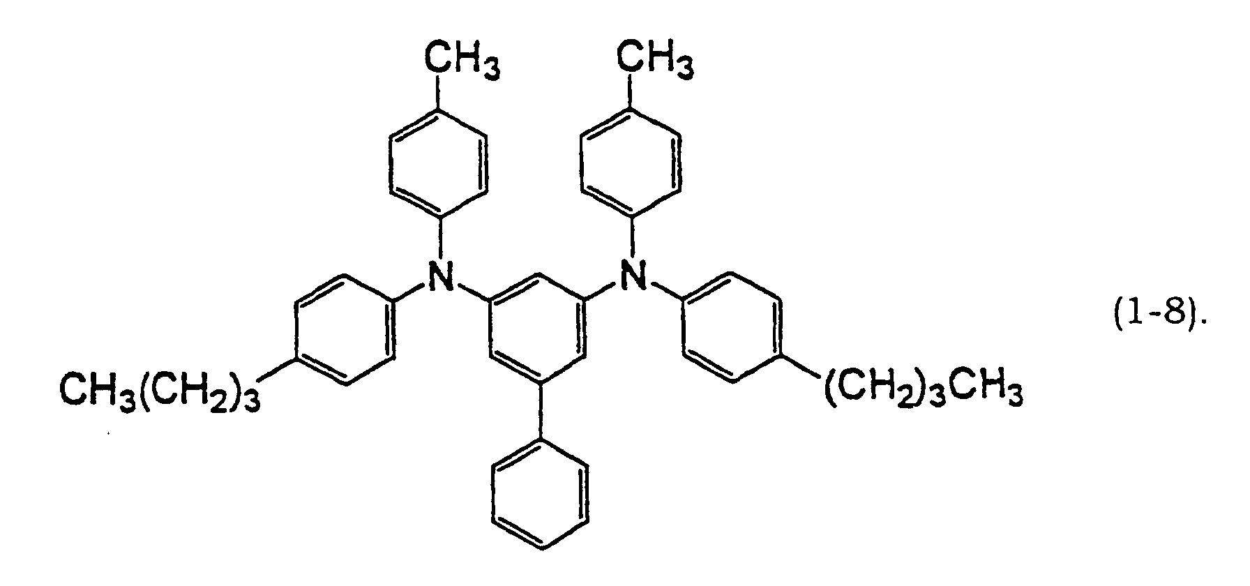
- a specific formula of m-phenylenediamine compounds (1) includes, for example, compounds (1-1) to (1-11) wherein each kind and each substitution position of the groups R 1A to R 1F in the formula (1) are as shown in Table 1, but is not limited thereto.
- Each position at which R 1C to R 2F are substituted on the phenyl group is a position represented by each small numeral in the following general formula (1).
- any construction of so-called single-layer type and multi-layer type photosensitive layers may be employed.
- the single-layer type photosensitive layer is characterized by the m-phenylenediamine compound (1) being contained as the hole transferring material in a binding resin, together with an electric charge generating material.
- Such a single-layer type photosensitive layer is capable of coping with any of positive and negative charging using a single construction, and has simple layer construction and is superior in productivity.
- the single-layer type photosensitive layer can contain an organic electron transferring material having an excellent electron transferring capabilityin addition to the above respective components. Such a photosensitive layer does not cause an interaction between the m-phenylenediamine compound (1) and electron transferring material and, therefore, the sensitivity is much higher.
- the multi-layer type photosensitive layer comprises an electric charge generating layer containing an electric charge generating material and an electric charge transferring layer containing an electric charge transferring material on a conductive substrate.
- the order of forming both layers may be optional.
- the film thickness of the electric charge generating layer is usually thinner than that of the electric charge transferring layer. Therefore, for protecting the electric charge generating layer, the electric charge generating layer is preferably formed on the conductive substrate and the electric charge transferring layer is formed thereon.
- the multi-layer type photosensitive layer becomes a positive or negative charging type.
- the m-phenylenediamine compound (1) which is the hole transferring material
- the resulting photosensitive layer becomes a negative charging type.
- the electron transferring material is contained in the electric charge generating layer, the sensitivity is further improved.
- the electron transferring material is used as the electric charge transferring material of the electric charge transferring layer in the multi-layer type photosensitive layer with the above layer construction, the resulting photosensitive layer becomes a positive charging type.
- the m-phenylenediamine compound (1) as the holetransferring material may be contained in the electric charge generating layer.
- the electric charge generating material, electron transferring material, hole transferring material and binding resin used in the electrophotosensitive material of the present invention are as follows.
- Examples of the electric charge generating material include compounds represented by the following general formulas (CG1) to (CG12) :
- examples of the alkyl group include the same groups as those described above.
- alkyl group examples include substituted or non-substituted alkyl groups having 18 or less carbon atoms, such as octyl, nonyl, decyl, dodecyl, tridecyl, pentadecyl, octadecyl, etc., in addition to the above alkyl groups having 1 to 6 carbon atoms.
- cycloalkyl group examples include groups having 3 to 8 carbon atoms, such as cyclopropyl, cyclobutyl, cyclopentyl, cyclohexyl, cycloheptyl, and cyclooctyl.
- alkoxy group examples include groups having 1 to 6 carbon atoms, such as methoxy, ethoxy, n-propoxy, isopropoxy, n-butoxy, isobutoxy, s-butoxy, t-butoxy, pentyloxy, and hexyloxy.
- aryl group examples include groups such as phenyl, tolyl, xylyl, naphthyl, anthryl, phenanthryl, fluorenyl, biphenylyl, and o-terphenyl.
- aralkyl group examples include groups such as benzyl, benzyhydryl, trityl, and phenethyl.
- alkanoyl group examples include groups such as formyl, acetyl, propionyl, butyryl, pentanoyl, and hexanoyl.
- heterocyclic group examples include thienyl, furyl, pyrrolyl, pyrrolidinyl, oxazolyl, isooxazolyl, thiazolyl, isothiazolyl, imidazolyl, 2H-imidazolyl, pyrazolyl, triazolyl, tetrazolyl, pyranyl, pyridyl, piperidyl, piperidino, 3-morpholinyl, morpholino, and thiazolyl.
- it may be a heterocyclic group condensed with an aromatic ring.
- substituents which may be substituted on the groups include halogen atoms, amino groups, hydroxyl groups, optionally esterified carboxyl groups, cyano groups, alkyl groups having 1 to 6 carbon atoms, alkoxy groups having 1 to 6 carbon atoms, alkenyl groups having 2 to 6 carbon atoms which may have an aryl group, etc.
- halogen atom examples include fluorine, chlorine, bromine and iodine.
- Examples of the coupler residue represented by Cp 1 , Cp 2 , Cp 3 , Cp 4 and Cp 5 include the groups shown in the following formulas (Cp-1) to (Cp-11).
- R g32 is a carbamoyl group, a sulfamoyl group, an allophanoyl group, oxamoyl group, anthranyloyl group, carbazoyl group, glycyl group, hydantoyl group, phthalamoyl group or a succinamoyl group.
- These groups may have one or more substituents such as halogen atoms, substituted or unsubstituted phenyl groups, substituted or unsubstituted naphthyl groups, nitro groups, cyano groups, alkyl groups, alkenyl groups, carbonyl groups, and carboxyl groups.
- R g33 is an atomic group which is required to form an aromatic ring, a polycyclic hydrocarbon or a heterocycle by condensing with a benzene ring. These rings may have one or more substituents as those described above.
- R g34 is an oxygen atom, a sulfur atom or an imino group.
- R g35 is a divalent chain hydrocarbon or aromatic hydrocarbon group. These groups may have one or more substituents as those described above.
- R g36 is an alkyl group, an aralkyl group, an aryl group or a heterocyclic group. These groups may have one or more substituents as those described above.
- R g37 is an atomic group which is required to form a heterocycle, together with a divalent chain hydrocarbon or aromatic hydrocarbon group, or two nitrogen atoms in the above formulas (Cp-7) to (Cp-10). These rings may have one or more substituents as those described above.
- R g38 is a hydrogen atom, an alkyl group, an amino group, a carbamoyl group, a sulfamoyl group, an allophanoyl group, a carboxyl group, an alkoxycarbonyl group, an aryl group or a cyano group.
- the groups other than the hydrogen atom may have one or more substituents as those described above.
- R g39 is an alkyl group or an aryl group. These groups may have one or more substituents as those described above.
- alkenyl group examples include alkenyl groups having 2 to 6 carbon atoms, such as vinyl, allyl, 2-butenyl, 3-butenyl, 1-methylallyl, 2-pentenyl, 2-hexenyl and the like.
- examples of the atomic group which is required to form an aromatic ring by condensing with a benzene ring include alkylene groups having 1 to 4 carbon atoms, such as methylene, ethylene, trimethylene, and tetramethylene.
- Examples of the aromatic ring to be formed by condensing the above R g33 with a benzene ring include naphthalene ring, anthracene ring, phenanthrene ring, pyrene ring, chrysene ring, and naphthacene ring.
- examples of the atomic group which is required to form a polycyclic hydrocarbon by condensing with a benzene ring include the above alkylene groups having 1 to 4 carbon atoms, or carbazole ring, benzocarbazole ring, and dibenzofuran ring.
- examples of the atomic group which is required to form a heterocycle by condensing with a benzene ring include benzofuranyl, benzothiophenyl, indolyl, 1H-indolyl, benzoxazolyl, benzothiazolyl, 1H-indadolyl, benzoimidazolyl, chromenyl, chromanyl, isochromanyl, quinolinyl, isoquinolinyl, cinnolinyl, phthalazinyl, quinazolinyl, quinoxalinyl, dibenzofuranyl, carbazolyl, xanthenyl, acridinyl, phenanthridinyl, phenazinyl, phenoxazinyl, and thianthrenyl.
- Examples of the aromatic heterocyclic group to be formed by condensing the above R g33 and the benzene ring include thienyl, furyl, pyrrolyl, oxazolyl, isoxazolyl, thiazolyl, isothiazolyl, imidazolyl, pyrazolyl, triazolyl, tetrazolyl, and pyridyl.
- it may also be a heterocyclic group condensed with other aromatic rings (e.g. benzofuranyl, benzoimidazolyl, benzoxazolyl, benzothiazolyl, quinolyl, etc.).
- examples of the divalent chain hydrocarbon include ethylene, trimethylene, and tetramethylene.
- examples of the divalent aromatic hydrocarbon include phenylene, naphthylene, and phenanthrylene.
- heterocyclic group examples include pyridyl, pyrazyl, thienyl, pyranyl, and indolyl.
- examples of the atomic group which is required to form a heterocycle, together with two nitrogen atoms include phenylene, naphthylene, phenanthrylene, ethylene, trimethylene, and tetramethylene.
- aromatic heterocyclic group to be formed by the above R g37 and two nitrogen atoms examples include benzoimidazole, benzo[f]benzoimidazole, dibenzo[e,g]benzoimidazole, and benzopyrimidine. These groups may respectively have the same group as that described above.
- examples of the alkoxycarbonyl group include methoxycarbonyl, ethoxycarbonyl, propoxycarbonyl, and butoxycarbonyl.
- inorganic photoconductive materials such as selenium, selenium-tellurium, selenium-arsenic, cadmium sulfide, amorphous silicon, etc.
- electric charge generating materials which have hitherto been known, such as pyrilium salts, anthanthrone pigments, triphenylmethane pigments, threne pigments, toluidine pigments, pyrazoline pigments, quinacridone pigments, etc., in addition to the above electric charge generating materials.
- the above electric charge generating materials can be used alone or in combination thereof to present an absorption wavelength within a desired range.
- a photosensitive material having sensitivity at the wavelength range of 700 nm or more is required in digital-optical image forming apparatus such as laser beam printers, facsimiles which used a semiconductor laser light source, etc. Therefore, phthalocyanine pigments such as metal-free phthalocyanine represented by the above formula (CG1), oxotitanyl phthalocyanine represented by the formula (CG2), etc. are preferably used.
- the crystal form of the above phthalocyanine pigments is not specifically limited, and various phthalocyanine pigments having different crystal form can be used.
- a photosensitive material having sensitivity at the visible range is required. Therefore, for example, the perylene pigment represented by the above general formula (CG3) and bisazo pigment represented by the general formula (CG4) are suitably used.
- Examples of the electron transferring material include compounds represented by the following general formulas (ET1) to (ET17) :
- examples of the halogenated alkyl group include those of which alkyl portions are various alkyl groups having 1 to 6 carbon atoms, such as chloromethyl, bromomethyl, fluoromethyl, iodomethyl, 2-chloroethyl, 1-fluoroethyl, 3-chloropropyl, 2-bromopropyl, 1-chloropropyl, 2-chloro-1-methylethyl, 1-bromo-1-methylethyl, 4-iodobutyl, 3-fluorobutyl, 3-chloro-2-methylpropyl, 2-iodo-2-methylpropyl, 1-fluoro-2-methylpropyl, 2-chloro-1,1-dimethylethyl, 2-bromo-1,1-dimethylethyl, 5-bromopentyl, and 4-chlorohexyl.
- alkyl portions are various alkyl groups having 1 to 6 carbon atoms, such as chloromethyl, bromo
- polycyclic aromatic group examples include naphthyl, penanthryl and anthryl.
- alkyl group examples include the same groups as those described above.
- aralkyloxycarbonyl group examples include those of which aralkyl portions are various aralkyl groups described above.
- N-alkylcarbamoyl group examples include those of which alkyl portions are various alkyl groups described above.
- dialkylamino group examples include those of which alkyl portions are various alkyl groups described above. Two alkyl groups substituted on the amino may be the same or different.
- substituents which may be substituted on the groups described above, include halogen atom, amino group, hydroxyl group, optionally esterified carboxyl group, cyano group, alkyl group having 1 to 6 carbon atoms, alkoxy group having 1 to 6 carbon atoms, and alkenyl having 2 to 6 carbon atoms which may have an aryl group.
- substitution position(s) of the substituents(s) are not specifically limited.
- electron transferring materials with the above-described electron transferring materials (ET1) to (ET17), or in place of them, which have hitherto been known, such as benzoquinone compounds, malononitrile, thiopyran compounds, tetracyanoethylene, 2,4,8-trinitrothioxanthone, dinitrobenzene, dinitroanthracene, dinitroacridine, nitroanthraquinone, dinitroanthraquinone, succinic anhydride, maleic anhydride, dibromomaleic anhydride, etc., in addition to those described above.
- benzoquinone compounds malononitrile
- thiopyran compounds tetracyanoethylene
- 2,4,8-trinitrothioxanthone dinitrobenzene, dinitroanthracene
- dinitroacridine nitroanthraquinone
- succinic anhydride maleic anhydride, dibromomaleic anhydride, etc.
- hole transferring materials which have hitherto been known, may be contained in the photosensitive layer, in addition to the above m-phenylenediamine compound (1) as a hole transferring material.
- Examples thereof include compounds represented by the following general formulas (HT1) to (HT13):
- examples of the alkyl group, alkoxy group and halogen atoms include the same groups as those described above.
- substituents which may be substituted on the groups include halogen atom, amino group, hydroxyl group, optionally esterified carboxyl group, cyano group, alkyl groups having 1 to 6 carbon atoms, alkoxy groups having 1 to 6 carbon atoms, alkenyl groups having 2 to 6 carbon atoms which may have an aryl group, etc.
- substitution positions (s) of the substituents(s) are not specifically limited.
- hole transferring materials with the above-described hole transferring materials (HT1) to (HT13), or in place of them, which have hitherto been known, that is, nitrogen-containing cyclic compounds and condensed polycyclic compounds, e.g.
- oxadiazole compounds such as 2,5-di(4-methylaminophenyl)-1,3,4- oxadiazole, etc.
- styryl compounds such as 9-(4- diethylaminostyryl)anthracene, etc.
- carbazole compounds such as polyvinyl carbazole, etc.; organopolysilane compounds; pyrazoline compounds such as 1-phenyl-3-(p- dimethylaminophenyl)pyrazoline, etc.; hydrazone compounds; triphenylamine compounds; indole compounds; oxazole compounds; isoxazole compounds; thiazole compounds; thiadiazole compounds; imidazole compounds; pyrazole compounds; and triazole compounds.
- these hole transferring materials may be used alone or in combination thereof.
- a binding resin is not required necessarily.
- thermoplastic resins such as styrene- butadiene copolymer, styrene-acrylonitrile copolymer, styrene- maleic acid copolymer, acrylic copolymer, styrene-acrylic acid copolymer, polyethylene, ethylene-vinyl acetate copolymer, chlorinated polyethylene, polyvinyl chloride, polypropylene, ionomer, vinyl chloride-vinyl acetate copolymer, polyester, alkyd resin, polyamide, polyurethane, polycarbonate, polyarylate, polysulfon, diaryl phthalate resin, ketone resin, polyvinylbutyral resin, polyether resin, polyester resin, etc.; crosslinking thermosetting resins such as silicone resin, epoxy resin, phenol resin, urea resin, melamine resin
- deterioration inhibitors e.g. antioxidants, radical scavengers, singlet quenchers, ultraviolet absorbers, etc.
- softeners plasticizers
- surface modifiers e.g., bulking agents, thickening agents, dispersion stabilizers, wax, acceptors, donors, etc.
- sensitizers such as terphenyl, halonaphthoquinones, acenaphthylene, etc. may be used in combination with the electric charge generating material.
- an electric charge generating material, a hole transferring material, a binding resin and an electron transferring material may be dissolved or dispersed in a suitable solvent, and the resulting coating solution is applied on a conductive substrate using means such as application, followed by drying.
- the electric charge generating material may be formulated in an amount of 0.1 to 50 parts by weight, preferably 0.5 to 30 parts by weight, based on 100 parts by weight of the binding resin.
- the electron transferring material may be formulated in an amount of 5 to 100 parts by weight, preferably 10 to 80 parts by weight, based on 100 parts by weight of the binding resin.
- the hole transferring material may be formulated in an amount of 5 to 500 parts by weight, preferably 25 to 200 parts by weight, based on 100 parts by weight of the binding resin.
- the electron transferring material is used with the hole transferring material
- the total amount of the hole transferring material and electron transferring material is 10 to 500 parts by weight, preferably 30 to 200 parts by weight, based on 100 parts by weight of the binding resin.
- the amount of the other electron transferring material is suitably 0.1 to 40 parts by weight, preferably 0.5 to 20 parts by weight, based on 100 parts by weight of the binding resin.
- the thickness of the single-layer type photosensitive material is preferably 5 to 100 ⁇ m, more preferably 10 to 50 ⁇ m.
- an electric charge generating layer containing an electric charge generating material may be formed on a conductive substrate using means such as deposition, application, etc., and then a coating solution containing an electron transferring material and a binding resin is applied on the electric charge generating layer using means such as application, followed by drying, to form an electric charge transferring layer.
- the electric charge generating material and binding resin which constitute the electric charge generating layer may be used in various proportions. It is suitable that the electric charge generating material is formulated in the amount of 5 to 1,000 parts by weight, preferably 30 to 500 parts by weight, based on 100 parts by weight of the binding resin. When a hole transferring material is contained in the electric charge generating layer, it is suitable that the hole trasferring material is formulated in the amount of 10 to 500 parts by weight, preferably 50 to 200 parts by weight, based on 100 parts by weight of the binding resin.
- the electron transferring material and binding resin, which constitute the electric charge transferring layer can be used in various proportions within such a range as not to prevent the transfer of electrons and to prevent the crystallization. It is suitable that the electron transferring material is used in the amount of 10 to 500 parts by weight, preferably 25 to 100 parts by weight, based on 100 parts by weight of the binding resin so as to easily transfer electrons generated by light irradiation in the electric charge generating layer.
- the amount of the other electron transferring material is suitably 0.1 to 40 parts by weight, preferably 0.5 to 20 parts by weight based on 100 parts by weight of the binding resin.
- the thickness of the electric charge generating layer is suitably about 0.01 to 5 ⁇ m, preferably about 0.1 to 3 ⁇ m, and that of the electric charge transferring layer is suitably 2 to 100 ⁇ m, preferably about 5 to 50 ⁇ m.
- a barrier layer may be formed, in such a range as not to injure the characteristics of the photosensitive material, between the conductive substrate and photosensitive layer in the single-layer type photosensitive material, or between the conductive substrate and electric charge generating layer or between the conductive substrate layer and electric charge transferring layer in the multi-layer type photosensitive material. Further, a protective layer may be formed on the surface of the photosensitive layer.
- the conductive substrate which may be used in the electrophotosensitive material of the present invention
- various materials having the conductivity include single metals such as iron aluminum, copper, tin, platinum, silver, vanadium, molybdenum, chromium, cadmium, titanium, nickel, palladium, indium, stainless steel, brass, etc.; plastic materials which are vapor-deposited or laminated with the above metal; glass materials coated with aluminum iodide, tin oxide, indium oxide, etc.
- the conductive substrate may be made in the form of a sheet or a drum to the construction of image-forming apparatus.
- the substrate itself may have a conductivity or only the surface of the substrate may have a conductivity. It is preferred that the conductive substrate has sufficient mechanical strength when used.
- the photosensitive layer may be produced by applying a dispersing (coating) solution, obtained by dissolving or dispersing a resin composition containing the above respective components in a suitable solvent, on a conductive substrate, followed by drying.
- a dispersing (coating) solution obtained by dissolving or dispersing a resin composition containing the above respective components in a suitable solvent
- the above electric charge generating material, electric charge transferring material and binding resin may be dispersed and mixed with a suitable solvent by a known method, for example, using a roll mill, a ball mill, an atriter, a paint shaker, a supersonic dispenser, etc. to prepare a dispersion, which is applied by a known means and then allowed to dry.
- the solvent for preparing the dispersing solution there can be used various organic solvents, and examples thereof include alcohols such as methanol, ethanol, isopropanol, butanol, etc.; aliphatic hydrocarbons such as n- hexane, octane, cyclohexane, etc.; aromatic hydrocarbons such as benzene, toluene, xylene, etc.; halogenated hydrocarbons such as dichloromethane, dichloroethane, chloroform, carbon tetrachloride, chlorobenzene, etc.; ethers such as dimethyl ether, diethyl ether, tetrahydrofuran, ethylene glycol dimethyl ether, diethylene glycol dimethyl ether, etc.; ketones such as acetone, methyl ethyl ketone, cyclohexanone, etc.; esters such as ethyl acetate, methyl acetate, etc.;
- surfactants In order to improve a dispersibility of the electric charge transferring material and electric charge generating material as well as a smoothness of the surface of the photosensitive layer, there may be used surfactants, leveling agents, etc.
- the image forming method of the present invention comprises the steps of uniformly charging the surface of the above electrophotosensitive material of the present invention, and exposing to light under the conditions of light exposure of not more than 0.54 mW/cm 2 and an exposure time of not more than 25 ms to form an electrostatic latent image on the surface, as described previously.
- the electrostatic latent image formed on the surface of the electrophotosensitive material is realised according to general method to form a toner image, transferred on the surface of a material for transfer such as paper and then fixed on the above transfer material, for example by means of heating or pressurizing.
- the electrophotosensitive material on which the toner image has been transferred is used for the subsequent image formation, usually after removing the residual toner on the surface using a cleaning blade.
- the electrophotosensitive material of the present invention can have high sensitivity, even such as has never been accomplished, as described above, it becomes possible to form a good image having a sufficient image concentration even under the exposure conditions capable of realizing higher speed and energy saving wherein the exposure dose is not more than 0.54 mW/cm 2 and the exposure time is not more than 25 ms.
- the light exposure may be determined as follows in the practical image forming device. For example, as shown in Fig. 1, exposure is performed in the state where a light receiving portion of a light detector 3 [e.g. Optical Block TQ82021, manufactured by Advantest Co., Ltd.] is located at the position of the center of an electrophotosensitive material 1 in a width direction out of the portion (indicated by a two-dot chain line in the drawing) to be exposed to light from a light source 2 on the surface of the electrophotosensitive material 1, that is, the position of a perpendicular (indicated by a one-dot chain line in the drawing) from the light source 2 on the electrophotosensitive material 1, and then the measured value is analyzed by using a analyzer 4 [e.g. Optical Power Meter TQ8215, manufactured by Advantest Co., Ltd.], thereby to obtain a light exposure.
- a light receiving portion of a light detector 3 e.g. Optical Block TQ82021, manufactured by Ad
- the exposure time is determined from an exposure width in the circumferential direction of the surface of the electrophotosensitive material 1 due to the light source 2, and a rotational rate of said electrophotosensitive material 1.
- the present invention can exert a specific working effect capable of providing an electrophotosensitive material which has a photosensitive layer not only having particularly high sensitivity and being able to sufficiently cope with the requirements such as realization of much higher speed and much larger energy saving of the image forming device, but also having excellent stability to strong light, durability and heat resistance, and an image forming method using the same, capable of realizing much higher speed and much larger energy saving.
- Electrophotosensitive material for analogue light source (single-layer type)
- a bisazo pigment represented by the formula (CG4-1) as the electric charge generating material
- 100 parts by weight of a m-phenylenediamine compound represented by the formula (1-1): as the hole transferring material and 100 parts by weight of poly(4,4'-cyclohexylidenediphenyl)carbonate as the binding resin were mixed and dispersed, together with a predetermined amount of tetrahydrofuran, by using an ultrasonic dispersion mixer to prepare a coating solution for single-layer type photosensitive layer.
- this coating solution was applied on an aluminum tube having an outer diameter of 78 mm and a length of 340 mm as the conductive substrate by using a dip coating method, followed by hot-air drying in a dark place at 100°C for 30 minutes to obtain a drum type electrophotosensitive material for analogue light source, which has a single-layer type photosensitive layer of 24 ⁇ m in film thickness.
- Example 2 According to the same manner as that described in Example 1 except for using 100 parts by weight of a m-phenylenediamine compound represented by the formula (1-2): as the hole transferring material, a drum type electrophotosensitive material for analogue light source, which has a single-layer type photosensitive layer, was produced.
- a drum type electrophotosensitive material for analogue light source which has a single-layer type photosensitive layer
- Example 1 According to the same manner as that described in Example 1 except for using 100 parts by weight of a m-phenylenediamine compound represented by the formula (1-3): as the hole transferring material, a drum type electrophotosensitive material for analogue light source, which has a single-layer type photosensitive layer, was produced.
- a drum type electrophotosensitive material for analogue light source which has a single-layer type photosensitive layer
- Example 1 According to the same manner as that described in Example 1 except for using 100 parts by weight of a m-phenylenediamine compound represented by the formula (1-4): as the hole transferring material, a drum type electrophotosensitive material for analogue light source, which has a single-layer type photosensitive layer, was produced.
- a drum type electrophotosensitive material for analogue light source which has a single-layer type photosensitive layer
- Example 2 According to the same manner as that described in Example 1 except for using 100 parts by weight of a m-phenylenediamine compound represented by the formula (1-5): as the hole transferring material, a drum type electrophotosensitive material for analogue light source, which has a single-layer type photosensitive layer, was produced.
- a drum type electrophotosensitive material for analogue light source which has a single-layer type photosensitive layer
- Example 1 According to the same manner as that described in Example 1 except for using 100 parts by weight of a m-phenylenediamine compound represented by the formula (1-6): as the hole transferring material, a drum type electrophotosensitive material for analogue light source, which has a single-layer type photosensitive layer, was produced.
- a drum type electrophotosensitive material for analogue light source which has a single-layer type photosensitive layer
- Example 7 According to the same manner as that described in Example 1 except for using 100 parts by weight of a m-phenylenediamine compound represented by the formula (1-7): as the hole transferring material, a drum type electrophotosensitive material for analogue light source, which has a single-layer type photosensitive layer, was produced.
- Example 1 According to the same manner as that described in Example 1 except for using 100 parts by weight of a m-phenylenediamine compound represented by the formula (1-9): as the hole transferring material, a drum type electrophotosensitive material for analogue light source, which has a single-layer type photosensitive layer, was produced.
- a drum type electrophotosensitive material for analogue light source which has a single-layer type photosensitive layer
- Example 1 According to the same manner as that described in Example 1 except for using 100 parts by weight of a m-phenylenediamine compound represented by the formula (1-10): as the hole transferring material, a drum type electrophotosensitive material for analogue light source, which has a single-layer type photosensitive layer, was produced.
- a drum type electrophotosensitive material for analogue light source which has a single-layer type photosensitive layer
- Example 1 According to the same manner as that described in Example 1 except for using 100 parts by weight of a m-phenylenediamine compound represented by the formula (1-11): as the hole transferring material, a drum type electrophotosensitive material for analogue light source, which has a single-layer type photosensitive layer, was produced.
- a drum type electrophotosensitive material for analogue light source which has a single-layer type photosensitive layer
- Example 1 According to the same manner as that described in Example 1 except for using 100 parts by weight of a m-phenylenediamine compound represented by the formula (3-1): which belongs to the compound of the fourth Synthesis Example of the publication of the prior application among the conventional m-phenylenediamine compound (3) as the hole transferring material, a drum type electrophotosensitive material for analogue light source, which has a single-layer type photosensitive layer, was produced.
- a drum type electrophotosensitive material for analogue light source which has a single-layer type photosensitive layer
- Example 2 According to the same manner as that described in Example 1 except for using 100 parts by weight of a m-phenylenediamine compound represented by the formula (4): wherein the outer phenyl group is substitute with a methoxy group which is a substituent other than a hydrogen atom and an alkyl group defined in the present invention, as the hole transferring material, a drum type electrophotosensitive material for analogue light source, which has a single-layer type photosensitive layer, was produced.
- a m-phenylenediamine compound represented by the formula (4): wherein the outer phenyl group is substitute with a methoxy group which is a substituent other than a hydrogen atom and an alkyl group defined in the present invention as the hole transferring material, a drum type electrophotosensitive material for analogue light source, which has a single-layer type photosensitive layer, was produced.
- Example 1 According to the same manner as that described in Example 1 except for using 100 parts by weight of a m-phenylenediamine compound represented by the formula (2-1): which belongs to the conventional m-phenylenediamine compound (2) as the hole transferring material, a drum type electrophotosensitive material for analogue light source, which has a single-layer type photosensitive layer, was produced.
- a m-phenylenediamine compound represented by the formula (2-1): which belongs to the conventional m-phenylenediamine compound (2) as the hole transferring material a drum type electrophotosensitive material for analogue light source, which has a single-layer type photosensitive layer, was produced.
- Example 2 According to the same manner as that described in Example 1 except for using 100 parts by weight of a m-phenylenediamine compound represented by the formula (2-2): which belongs to the conventional m-phenylenediamine compound (2) as the hole transferring material, a drum type electrophotosensitive material for analogue light source, which has a single-layer type photosensitive layer, was produced.
- a m-phenylenediamine compound represented by the formula (2-2): which belongs to the conventional m-phenylenediamine compound (2) as the hole transferring material a drum type electrophotosensitive material for analogue light source, which has a single-layer type photosensitive layer, was produced.
- Example 2 According to the same manner as that described in Example 1 except for using 100 parts by weight of a m-phenylenediamine compound represented by the formula (2-3): which belongs to the conventional m-phenylenediamine compound (2) as the hole transferring material, a drum type electrophotosensitive material for analogue light source, which has a single-layer type photosensitive layer, was produced.
- a m-phenylenediamine compound represented by the formula (2-3) which belongs to the conventional m-phenylenediamine compound (2) as the hole transferring material
- Example 2 According to the same manner as that described in Example 1 except for using 100 parts by weight of a m-phenylenediamine compound represented by the formula (5): wherein a chlorine atom which is a group other than that defined in the publication of the prior application is substituted on the 5-position of the central benzene ring, as the hole transferring material, a drum type electrophotosensitive material for analogue light source, which has a single-layer type photosensitive layer, was produced.
- a m-phenylenediamine compound represented by the formula (5): wherein a chlorine atom which is a group other than that defined in the publication of the prior application is substituted on the 5-position of the central benzene ring, as the hole transferring material a drum type electrophotosensitive material for analogue light source, which has a single-layer type photosensitive layer, was produced.
- the above electrophotosensitive material in the charged state was exposed (exposure time: 25 msec) by irradiating white light (light exposure: 0.54 mW/cm 2 ) from a halogen lamp which is a light source of the above mentioned test machine on the surface.
- the above exposure condition corresponds to an exposure condition in a high-speed image forming device wherein an image forming speed is 40 copies per minute as double as that of a current model.
- Each photosensitive layer of the electrophotosensitive materials of the respective Examples and Comparative Examples was peeled off in the form of a film (about 5 mg), put in an aluminum pan and then sealed to obtain a sample.
- the glass transition temperature [Tig (extrapolated glass transition initiation temperature °C), JIS K7121] of the photosensitive layer was measured under the conditions (atmospheric gas: air, heating rate: 20 °C/min.) using a differential scanning calorimeter (DSC) device [DSC8230D, manufactured by Rigaku Denki Co., Ltd.].
- the coating solution for single-layer type photosensitive layer prepared in the respective Examples and Comparative Examples was applied on an aluminum tube having an outer diameter of 30 mm and a length of 346 mm as the conductive substrate by using a dip coating method, followed by hot-air drying in a dark place at 100 °C for 30 minutes to obtain a drum type electrophotosensitive material for analogue light source, which has a single-layer type photosensitive layer of 24 ⁇ m in film thickness, used for high-temperature durability test.
- each electrophotosensitive material was mounted in a drum unit for an electrostatic copying machine [DC-2355, manufactured by Mita Industries Co., Ltd.] and was stored in an oven at 50 °C for a week in the state where a cleaning blade is always contacted with the surface.
- the linear pressure in case of pressing the cleaning blade was 30 N/cm 2 .
- this drum unit was mounted in the above electrostatic copying machine and copying of a gray scale image was performed.
- the formed image was visually observed and evaluated by the following criteria.
- An electrophotosensitive material using the compound of the formula (2-1) belonging to the conventional m-phenylenediamine compounds (2) as the hole transferring material of Comparative Example 3 and an electrophotosensitive material using the compound of the formula (5) corresponding to a compound obtained by substituting a chlorine atom on the 5-position of the central benzene ring of the compound of the formula (2-1) of Comparative Example 6 showed low initial sensitivity and, furthermore, the stability to strong light, durability and heat resistance were insufficient.
- electrophotosensitive materials using a m-phenylenediamine compound of the formula (1) of Examples 1 to 11 of the present invention have high initial sensitivity and are superior in stability to strong light, durability and heat resistance.
- the above electrophotosensitive material with the charged state was exposed (exposure time: 25 msec) by irradiating white light (light exposure: 0.92 mW/cm 2 ) from a halogen lamp as an exposure light source of the above tester on the surface.
- the above exposure condition corresponds to an exposure condition in an image forming speed wherein the image forming rate is 20 copies per minute of a current model.
- the electrophotosensitive material of the present invention has sufficient sensitivity even if it is used in an image forming device capable of realizing higher speed and energy saving wherein the exposure dose is not more than 0.54 mW/cm 2 and the exposure time is not more than 25 msec.
Landscapes
- Physics & Mathematics (AREA)
- General Physics & Mathematics (AREA)
- Photoreceptors In Electrophotography (AREA)
- Exposure Or Original Feeding In Electrophotography (AREA)
Claims (10)
- Elektrophotosensitives Material, das eine lichtempfindliche Schicht aufweist, die eine m-Phenylendiamin-Verbindung der allgemeinen Formel ( 1 ) enthält,in der bedeuten:
 R1A und R1B, die gleich oder verschieden sein können, eine Alkylgruppe
undR1C, R1D, R1E und R1F, die gleich oder verschieden sein können, ein Wasserstoffatom oder eine Alkylgruppe. - Elektrophotosensitives Material nach Anspruch 1, wobei die Gruppen R1A und R1B in der allgemeinen Formel (1) eine Alkylgruppe mit 1 bis 4 Kohlenstoffatomen, die Gruppen R1C und R1F eine Alkylgruppe mit 1 bis 4 Kohlenstoffatomen, die als Substituent in 3- oder 4-Stellung einer Phenylgruppe vorliegt, und die Gruppen R1D und R1E ein Wasserstoffatom bedeuten.
- Elektrophotosensitives Material nach Anspruch 2, wobei die jeder der Gruppen R1A, R1B, R1C und R1F entsprechende Alkylgruppe Methyl, Isopropyl oder n-Butyl ist.
- Elektrophotosensitives Material nach Anspruch 3, wobei die m-Phenylendiamin-Verbindung, die in der lichtempfindlichen Schicht enthalten ist, eine Verbindung der Formel (1-2) ist:

- Elektrophotosensitives Material nach Anspruch 3, wobei die m-Phenylendiamin-Verbindung, die in der lichtempfindlichen Schicht enthalten ist, eine Verbindung der Formel (1-5) ist:

- Elektrophotosensitives Material nach Anspruch 3, wobei die m-Phenylendiamin-Verbindung, die in der lichtempfindlichen Schicht enthalten ist, eine Verbindung der Formel (1-8) ist:
- Elektrophotosensitives Material nach Anspruch 3, wobei die m-Phenylendiamin-Verbindung, die in der lichtempfindlichen Schicht enthalten ist, eine Verbindung der Formel (1-10) ist:

- Verwendung eines elektrophotosensitiven Materials nach einem oder mehreren der vorhergehenden Ansprüche in einer Bilderzeugungsvorrichtung, in der die Belichtungsstärke des elektrophotosensitiven Material ausgesetzt wird, nicht mehr als 0,54 mW/cm2 und die Belichtungszeit nicht mehr als 25 ms betragen.
- Verfahren zur Bilderzeugung, das folgende Schritte umfasst:gleichmäßiges Aufladen der Oberfläche eines elektrophotosensitiven Materials, das eine lichtempfindliche Schicht aufweist, die eine m-Phenylendiamin-Verbindung der allgemeinen Formel (1)
 enthält, in der bedeuten: R1A und R1B, die gleich oder verschieden sein können, eine Alkylgruppe
undR1C, R1D, R1E und R1F, die gleich oder verschieden sein können, ein Wasserstoffatom oder eine Alkylgruppe,
undBelichten unter Bedingungen, die einer Belichtungsstärke von nicht mehr als 0,54 mW/cm2 und einer Belichtungszeit von nicht mehr als 25 ms betragen, unter Erzeugung eines elektrostatischen latenten Bildes auf der Oberfläche. - Verfahren zur Bilderzeugung nach Anspruch 9, das ferner folgende Schritte umfasst:Entwickeln des auf der Oberfläche des elektrophotosensitiven Materials gebildeten latenten Bildes mit einem Entwickler, der einen Toner enthält, unter Umwandlung des elektrostatischen latenten Bildes in ein Tonerbild,Übertragen des Tonerbildes auf die Oberfläche eines Übertragungsmaterials undFixieren des Tonerbildes.
Applications Claiming Priority (2)
| Application Number | Priority Date | Filing Date | Title |
|---|---|---|---|
| JP35863397A JP3174022B2 (ja) | 1997-12-25 | 1997-12-25 | 電子写真感光体とそれを用いた画像形成方法 |
| JP35863397 | 1997-12-25 |
Publications (2)
| Publication Number | Publication Date |
|---|---|
| EP0926558A1 EP0926558A1 (de) | 1999-06-30 |
| EP0926558B1 true EP0926558B1 (de) | 2004-02-25 |
Family
ID=18460326
Family Applications (1)
| Application Number | Title | Priority Date | Filing Date |
|---|---|---|---|
| EP98310746A Expired - Lifetime EP0926558B1 (de) | 1997-12-25 | 1998-12-24 | Elektrophotosensitives Material und Verfahren zur Bilderzeugung unter Verwendung dieses Materials |
Country Status (8)
| Country | Link |
|---|---|
| US (1) | US6015646A (de) |
| EP (1) | EP0926558B1 (de) |
| JP (1) | JP3174022B2 (de) |
| CN (1) | CN1180316C (de) |
| AU (1) | AU9713498A (de) |
| CA (1) | CA2256641A1 (de) |
| DE (1) | DE69821894T2 (de) |
| TW (1) | TW407226B (de) |
Families Citing this family (8)
| Publication number | Priority date | Publication date | Assignee | Title |
|---|---|---|---|---|
| JP3646012B2 (ja) * | 1998-10-29 | 2005-05-11 | 京セラミタ株式会社 | 電子写真感光体 |
| JP2000314969A (ja) * | 1999-04-30 | 2000-11-14 | Fuji Denki Gazo Device Kk | 電子写真用感光体および電子写真装置 |
| JP3583705B2 (ja) * | 2000-09-26 | 2004-11-04 | 京セラミタ株式会社 | 電子写真感光体 |
| JP2002131961A (ja) * | 2000-10-26 | 2002-05-09 | Kyocera Mita Corp | 電子写真感光体およびその製造方法 |
| JP2007093764A (ja) * | 2005-09-27 | 2007-04-12 | Kyocera Mita Corp | フェニレンジアミン化合物および電子写真感光体 |
| US7662526B2 (en) * | 2007-05-04 | 2010-02-16 | Xerox Corporation | Photoconductors |
| JP5270253B2 (ja) * | 2008-08-07 | 2013-08-21 | 京セラドキュメントソリューションズ株式会社 | 電子写真感光体及び画像形成装置 |
| JP5696124B2 (ja) * | 2012-10-31 | 2015-04-08 | 京セラドキュメントソリューションズ株式会社 | 電子写真感光体及び画像形成装置 |
Family Cites Families (12)
| Publication number | Priority date | Publication date | Assignee | Title |
|---|---|---|---|---|
| JP2504790B2 (ja) * | 1987-11-30 | 1996-06-05 | 三田工業株式会社 | 電子写真感光体用電荷輸送材料 |
| JPH03236269A (ja) * | 1990-02-14 | 1991-10-22 | Fujitsu Miyagi Electron:Kk | リードフレーム |
| JPH03261958A (ja) * | 1990-03-13 | 1991-11-21 | Mita Ind Co Ltd | 電子写真感光体 |
| DE69112898T2 (de) * | 1990-05-02 | 1996-06-13 | Mita Industrial Co Ltd | Meta-Phenylendiaminverbindung und elektrophotoempfindliches Material, das diese Verbindung verwendet. |
| JPH04300853A (ja) * | 1991-03-29 | 1992-10-23 | Mita Ind Co Ltd | フェニレンジアミン誘導体及びそれを用いた感光体 |
| JP2953126B2 (ja) * | 1991-07-31 | 1999-09-27 | ミノルタ株式会社 | 新規なフェニレンジアミン化合物およびそれを用いた感光体 |
| US5334470A (en) * | 1991-09-02 | 1994-08-02 | Ricoh Company, Ltd. | Electrophotographic element with M-phenylenediamine derivatives therein |
| JP3435476B2 (ja) * | 1991-09-25 | 2003-08-11 | 株式会社リコー | 電子写真用感光体 |
| US5494765A (en) * | 1993-01-14 | 1996-02-27 | Mita Industrial Co. Ltd | Electrophotosensitive material using a phenylenediamine derivative |
| JPH0772634A (ja) * | 1993-06-24 | 1995-03-17 | Ricoh Co Ltd | 電子写真感光体 |
| JPH07324058A (ja) * | 1994-05-30 | 1995-12-12 | Mita Ind Co Ltd | m−フェニレンジアミン誘導体およびそれを用いた電子写真感光体 |
| JPH089579A (ja) * | 1994-06-20 | 1996-01-12 | Fujitsu General Ltd | 電動機 |
-
1997
- 1997-12-25 JP JP35863397A patent/JP3174022B2/ja not_active Expired - Lifetime
-
1998
- 1998-12-14 US US09/210,612 patent/US6015646A/en not_active Expired - Lifetime
- 1998-12-16 AU AU97134/98A patent/AU9713498A/en not_active Abandoned
- 1998-12-17 TW TW087121089A patent/TW407226B/zh not_active IP Right Cessation
- 1998-12-17 CA CA002256641A patent/CA2256641A1/en not_active Abandoned
- 1998-12-24 DE DE69821894T patent/DE69821894T2/de not_active Expired - Lifetime
- 1998-12-24 EP EP98310746A patent/EP0926558B1/de not_active Expired - Lifetime
- 1998-12-25 CN CNB981117295A patent/CN1180316C/zh not_active Expired - Fee Related
Also Published As
| Publication number | Publication date |
|---|---|
| CN1221133A (zh) | 1999-06-30 |
| EP0926558A1 (de) | 1999-06-30 |
| TW407226B (en) | 2000-10-01 |
| DE69821894T2 (de) | 2005-01-05 |
| CN1180316C (zh) | 2004-12-15 |
| JP3174022B2 (ja) | 2001-06-11 |
| AU9713498A (en) | 1999-07-15 |
| DE69821894D1 (de) | 2004-04-01 |
| CA2256641A1 (en) | 1999-06-25 |
| US6015646A (en) | 2000-01-18 |
| JPH11190909A (ja) | 1999-07-13 |
Similar Documents
| Publication | Publication Date | Title |
|---|---|---|
| JP3272257B2 (ja) | 電子写真感光体 | |
| JP2000226354A (ja) | キノン誘導体およびこれを用いた電子写真感光体 | |
| JP3530702B2 (ja) | ジチオマレイン酸イミド誘導体を用いた電子写真感光体 | |
| EP0926558B1 (de) | Elektrophotosensitives Material und Verfahren zur Bilderzeugung unter Verwendung dieses Materials | |
| JP3571165B2 (ja) | ナフトキノン誘導体を用いた電子写真感光体 | |
| JP3720927B2 (ja) | スチルベン誘導体およびそれを用いた電子写真感光体 | |
| JP3668054B2 (ja) | キノン誘導体およびこれを用いた電子写真感光体 | |
| JP3375849B2 (ja) | ナフトキノン誘導体およびこれを用いた電子写真感光体 | |
| JP3246879B2 (ja) | 電子写真感光体 | |
| JP3269981B2 (ja) | 電子写真感光体 | |
| JP3264618B2 (ja) | 電子写真感光体 | |
| JP3260728B2 (ja) | ナフトキノン誘導体を用いた電子写真感光体 | |
| JP3315337B2 (ja) | ナフトキノン誘導体を用いた電子写真感光体 | |
| JPH10246973A (ja) | 電子写真感光体 | |
| JPH10324658A (ja) | ナフトキノン誘導体およびこれを用いた電子写真感光体 | |
| JPH10104858A (ja) | 電子写真感光体 | |
| JPH0627700A (ja) | 電子写真感光体 | |
| JPH0611872A (ja) | 電子写真感光体 | |
| JPH0611871A (ja) | 電子写真感光体 | |
| JPH07146573A (ja) | 電子写真感光体 | |
| JPH0627701A (ja) | 電子写真感光体 | |
| JPH07146567A (ja) | 電子写真感光体 | |
| JPH07146571A (ja) | 電子写真感光体 | |
| JPH07146568A (ja) | 電子写真感光体 | |
| JPH07146569A (ja) | 電子写真感光体 |
Legal Events
| Date | Code | Title | Description |
|---|---|---|---|
| PUAI | Public reference made under article 153(3) epc to a published international application that has entered the european phase |
Free format text: ORIGINAL CODE: 0009012 |
|
| AK | Designated contracting states |
Kind code of ref document: A1 Designated state(s): CH DE GB LI |
|
| AX | Request for extension of the european patent |
Free format text: AL;LT;LV;MK;RO;SI |
|
| 17P | Request for examination filed |
Effective date: 19990818 |
|
| AKX | Designation fees paid |
Free format text: CH DE GB LI |
|
| RAP1 | Party data changed (applicant data changed or rights of an application transferred) |
Owner name: KYOCERA MITA CORPORATION |
|
| GRAP | Despatch of communication of intention to grant a patent |
Free format text: ORIGINAL CODE: EPIDOSNIGR1 |
|
| GRAS | Grant fee paid |
Free format text: ORIGINAL CODE: EPIDOSNIGR3 |
|
| GRAA | (expected) grant |
Free format text: ORIGINAL CODE: 0009210 |
|
| AK | Designated contracting states |
Kind code of ref document: B1 Designated state(s): CH DE GB LI |
|
| REG | Reference to a national code |
Ref country code: GB Ref legal event code: FG4D |
|
| REG | Reference to a national code |
Ref country code: CH Ref legal event code: EP |
|
| REF | Corresponds to: |
Ref document number: 69821894 Country of ref document: DE Date of ref document: 20040401 Kind code of ref document: P |
|
| REG | Reference to a national code |
Ref country code: CH Ref legal event code: NV Representative=s name: ISLER & PEDRAZZINI AG |
|
| PLBE | No opposition filed within time limit |
Free format text: ORIGINAL CODE: 0009261 |
|
| STAA | Information on the status of an ep patent application or granted ep patent |
Free format text: STATUS: NO OPPOSITION FILED WITHIN TIME LIMIT |
|
| 26N | No opposition filed |
Effective date: 20041126 |
|
| REG | Reference to a national code |
Ref country code: CH Ref legal event code: PCAR Free format text: ISLER & PEDRAZZINI AG;POSTFACH 1772;8027 ZUERICH (CH) |
|
| PGFP | Annual fee paid to national office [announced via postgrant information from national office to epo] |
Ref country code: GB Payment date: 20101222 Year of fee payment: 13 |
|
| PGFP | Annual fee paid to national office [announced via postgrant information from national office to epo] |
Ref country code: CH Payment date: 20111213 Year of fee payment: 14 |
|
| PGFP | Annual fee paid to national office [announced via postgrant information from national office to epo] |
Ref country code: DE Payment date: 20111221 Year of fee payment: 14 |
|
| REG | Reference to a national code |
Ref country code: CH Ref legal event code: PL |
|
| GBPC | Gb: european patent ceased through non-payment of renewal fee |
Effective date: 20121224 |
|
| REG | Reference to a national code |
Ref country code: DE Ref legal event code: R119 Ref document number: 69821894 Country of ref document: DE Effective date: 20130702 |
|
| PG25 | Lapsed in a contracting state [announced via postgrant information from national office to epo] |
Ref country code: LI Free format text: LAPSE BECAUSE OF NON-PAYMENT OF DUE FEES Effective date: 20121231 Ref country code: CH Free format text: LAPSE BECAUSE OF NON-PAYMENT OF DUE FEES Effective date: 20121231 Ref country code: DE Free format text: LAPSE BECAUSE OF NON-PAYMENT OF DUE FEES Effective date: 20130702 |
|
| PG25 | Lapsed in a contracting state [announced via postgrant information from national office to epo] |
Ref country code: GB Free format text: LAPSE BECAUSE OF NON-PAYMENT OF DUE FEES Effective date: 20121224 |