EP0926698A2 - Flacher Bildschirm mit Elektronenemittern - Google Patents
Flacher Bildschirm mit Elektronenemittern Download PDFInfo
- Publication number
- EP0926698A2 EP0926698A2 EP98124545A EP98124545A EP0926698A2 EP 0926698 A2 EP0926698 A2 EP 0926698A2 EP 98124545 A EP98124545 A EP 98124545A EP 98124545 A EP98124545 A EP 98124545A EP 0926698 A2 EP0926698 A2 EP 0926698A2
- Authority
- EP
- European Patent Office
- Prior art keywords
- electrodes
- electron emission
- thin
- flat panel
- display apparatus
- Prior art date
- Legal status (The legal status is an assumption and is not a legal conclusion. Google has not performed a legal analysis and makes no representation as to the accuracy of the status listed.)
- Withdrawn
Links
- 239000000758 substrate Substances 0.000 claims abstract description 120
- 229910052751 metal Inorganic materials 0.000 claims abstract description 92
- 239000002184 metal Substances 0.000 claims abstract description 92
- 239000010409 thin film Substances 0.000 claims abstract description 74
- 239000000463 material Substances 0.000 claims abstract description 44
- 239000012212 insulator Substances 0.000 claims abstract description 29
- 239000004065 semiconductor Substances 0.000 claims abstract description 3
- 238000000034 method Methods 0.000 description 18
- -1 LiOx Chemical class 0.000 description 16
- 229910052710 silicon Inorganic materials 0.000 description 14
- XUIMIQQOPSSXEZ-UHFFFAOYSA-N Silicon Chemical compound [Si] XUIMIQQOPSSXEZ-UHFFFAOYSA-N 0.000 description 13
- 239000010703 silicon Substances 0.000 description 13
- 238000004519 manufacturing process Methods 0.000 description 12
- 239000011159 matrix material Substances 0.000 description 12
- 239000010408 film Substances 0.000 description 11
- VYPSYNLAJGMNEJ-UHFFFAOYSA-N Silicium dioxide Chemical compound O=[Si]=O VYPSYNLAJGMNEJ-UHFFFAOYSA-N 0.000 description 10
- 239000010931 gold Substances 0.000 description 10
- 230000015572 biosynthetic process Effects 0.000 description 9
- BASFCYQUMIYNBI-UHFFFAOYSA-N platinum Chemical compound [Pt] BASFCYQUMIYNBI-UHFFFAOYSA-N 0.000 description 9
- 229910052782 aluminium Inorganic materials 0.000 description 7
- 239000010949 copper Substances 0.000 description 7
- 230000000694 effects Effects 0.000 description 7
- 239000011521 glass Substances 0.000 description 7
- 229920001721 polyimide Polymers 0.000 description 7
- 229910052814 silicon oxide Inorganic materials 0.000 description 7
- 239000011651 chromium Substances 0.000 description 6
- 229910052697 platinum Inorganic materials 0.000 description 6
- 238000007650 screen-printing Methods 0.000 description 6
- 238000004544 sputter deposition Methods 0.000 description 6
- 239000004642 Polyimide Substances 0.000 description 5
- 229910021417 amorphous silicon Inorganic materials 0.000 description 5
- 229910052804 chromium Inorganic materials 0.000 description 5
- 229910052802 copper Inorganic materials 0.000 description 5
- 229910052737 gold Inorganic materials 0.000 description 5
- 238000007740 vapor deposition Methods 0.000 description 5
- 238000005229 chemical vapour deposition Methods 0.000 description 4
- 239000003086 colorant Substances 0.000 description 4
- 238000005530 etching Methods 0.000 description 4
- 239000011810 insulating material Substances 0.000 description 4
- 125000006850 spacer group Chemical group 0.000 description 4
- 239000000126 substance Substances 0.000 description 4
- VYZAMTAEIAYCRO-UHFFFAOYSA-N Chromium Chemical compound [Cr] VYZAMTAEIAYCRO-UHFFFAOYSA-N 0.000 description 3
- XAGFODPZIPBFFR-UHFFFAOYSA-N aluminium Chemical compound [Al] XAGFODPZIPBFFR-UHFFFAOYSA-N 0.000 description 3
- PNEYBMLMFCGWSK-UHFFFAOYSA-N aluminium oxide Inorganic materials [O-2].[O-2].[O-2].[Al+3].[Al+3] PNEYBMLMFCGWSK-UHFFFAOYSA-N 0.000 description 3
- 229910052593 corundum Inorganic materials 0.000 description 3
- PXHVJJICTQNCMI-UHFFFAOYSA-N nickel Substances [Ni] PXHVJJICTQNCMI-UHFFFAOYSA-N 0.000 description 3
- 229910052721 tungsten Inorganic materials 0.000 description 3
- 229910001845 yogo sapphire Inorganic materials 0.000 description 3
- 229910000838 Al alloy Inorganic materials 0.000 description 2
- XMWRBQBLMFGWIX-UHFFFAOYSA-N C60 fullerene Chemical compound C12=C3C(C4=C56)=C7C8=C5C5=C9C%10=C6C6=C4C1=C1C4=C6C6=C%10C%10=C9C9=C%11C5=C8C5=C8C7=C3C3=C7C2=C1C1=C2C4=C6C4=C%10C6=C9C9=C%11C5=C5C8=C3C3=C7C1=C1C2=C4C6=C2C9=C5C3=C12 XMWRBQBLMFGWIX-UHFFFAOYSA-N 0.000 description 2
- 229910005451 FeTiO3 Inorganic materials 0.000 description 2
- 229910005831 GeO3 Inorganic materials 0.000 description 2
- 229910026161 MgAl2O4 Inorganic materials 0.000 description 2
- 229910017676 MgTiO3 Inorganic materials 0.000 description 2
- 229910004205 SiNX Inorganic materials 0.000 description 2
- 229910004273 TeO3 Inorganic materials 0.000 description 2
- 229910010252 TiO3 Inorganic materials 0.000 description 2
- 229910045601 alloy Inorganic materials 0.000 description 2
- 239000000956 alloy Substances 0.000 description 2
- 125000004429 atom Chemical group 0.000 description 2
- 229910052799 carbon Inorganic materials 0.000 description 2
- 125000004432 carbon atom Chemical group C* 0.000 description 2
- 239000003989 dielectric material Substances 0.000 description 2
- 230000005684 electric field Effects 0.000 description 2
- 239000012777 electrically insulating material Substances 0.000 description 2
- 229910003472 fullerene Inorganic materials 0.000 description 2
- PCHJSUWPFVWCPO-UHFFFAOYSA-N gold Chemical compound [Au] PCHJSUWPFVWCPO-UHFFFAOYSA-N 0.000 description 2
- 238000010438 heat treatment Methods 0.000 description 2
- 239000012535 impurity Substances 0.000 description 2
- 229910052738 indium Inorganic materials 0.000 description 2
- 229910052741 iridium Inorganic materials 0.000 description 2
- 150000002739 metals Chemical class 0.000 description 2
- 238000001451 molecular beam epitaxy Methods 0.000 description 2
- 229910052759 nickel Inorganic materials 0.000 description 2
- 150000004767 nitrides Chemical class 0.000 description 2
- 229920002120 photoresistant polymer Polymers 0.000 description 2
- HBMJWWWQQXIZIP-UHFFFAOYSA-N silicon carbide Chemical compound [Si+]#[C-] HBMJWWWQQXIZIP-UHFFFAOYSA-N 0.000 description 2
- 229910010271 silicon carbide Inorganic materials 0.000 description 2
- 238000009751 slip forming Methods 0.000 description 2
- 229910052596 spinel Inorganic materials 0.000 description 2
- 239000010936 titanium Substances 0.000 description 2
- WFKWXMTUELFFGS-UHFFFAOYSA-N tungsten Chemical compound [W] WFKWXMTUELFFGS-UHFFFAOYSA-N 0.000 description 2
- 239000010937 tungsten Substances 0.000 description 2
- NNDLQUNWZOIESH-UHFFFAOYSA-N 8-hydroxy-7-[[7-[(8-hydroxy-5-sulfoquinoline-7-carbonyl)amino]-4-[3-[(8-hydroxy-5-sulfoquinoline-7-carbonyl)amino]propyl]heptyl]carbamoyl]quinoline-5-sulfonic acid Chemical compound C1=CC=NC2=C(O)C(C(=O)NCCCC(CCCNC(=O)C=3C(=C4N=CC=CC4=C(C=3)S(O)(=O)=O)O)CCCNC(=O)C3=C(C4=NC=CC=C4C(=C3)S(O)(=O)=O)O)=CC(S(O)(=O)=O)=C21 NNDLQUNWZOIESH-UHFFFAOYSA-N 0.000 description 1
- 229910017988 AgVO3 Inorganic materials 0.000 description 1
- 229910000505 Al2TiO5 Inorganic materials 0.000 description 1
- 229910016384 Al4C3 Inorganic materials 0.000 description 1
- 229910017083 AlN Inorganic materials 0.000 description 1
- 229910017107 AlOx Inorganic materials 0.000 description 1
- 229910017257 AsOx Inorganic materials 0.000 description 1
- 229910052580 B4C Inorganic materials 0.000 description 1
- 229910016010 BaAl2 Inorganic materials 0.000 description 1
- 229910002771 BaFe12O19 Inorganic materials 0.000 description 1
- 229910015805 BaWO4 Inorganic materials 0.000 description 1
- ZOXJGFHDIHLPTG-UHFFFAOYSA-N Boron Chemical compound [B] ZOXJGFHDIHLPTG-UHFFFAOYSA-N 0.000 description 1
- 229910014813 CaC2 Inorganic materials 0.000 description 1
- 229910002971 CaTiO3 Inorganic materials 0.000 description 1
- 229910004829 CaWO4 Inorganic materials 0.000 description 1
- 229910002976 CaZrO3 Inorganic materials 0.000 description 1
- OKTJSMMVPCPJKN-UHFFFAOYSA-N Carbon Chemical compound [C] OKTJSMMVPCPJKN-UHFFFAOYSA-N 0.000 description 1
- 229910004605 CdOx Inorganic materials 0.000 description 1
- 229910004607 CdSnO3 Inorganic materials 0.000 description 1
- 229910004613 CdTe Inorganic materials 0.000 description 1
- 229910002979 CdTiO3 Inorganic materials 0.000 description 1
- 229910003320 CeOx Inorganic materials 0.000 description 1
- 229910052684 Cerium Inorganic materials 0.000 description 1
- 229910021556 Chromium(III) chloride Inorganic materials 0.000 description 1
- 229910002518 CoFe2O4 Inorganic materials 0.000 description 1
- 229910018864 CoMoO4 Inorganic materials 0.000 description 1
- 229910002451 CoOx Inorganic materials 0.000 description 1
- 229910019096 CoTiO3 Inorganic materials 0.000 description 1
- 229910019408 CoWO4 Inorganic materials 0.000 description 1
- RYGMFSIKBFXOCR-UHFFFAOYSA-N Copper Chemical compound [Cu] RYGMFSIKBFXOCR-UHFFFAOYSA-N 0.000 description 1
- 229910021589 Copper(I) bromide Inorganic materials 0.000 description 1
- 229910019923 CrOx Inorganic materials 0.000 description 1
- VMQMZMRVKUZKQL-UHFFFAOYSA-N Cu+ Chemical compound [Cu+] VMQMZMRVKUZKQL-UHFFFAOYSA-N 0.000 description 1
- 229910002477 CuCr2O4 Inorganic materials 0.000 description 1
- 229910016516 CuFe2O4 Inorganic materials 0.000 description 1
- 229910016547 CuNx Inorganic materials 0.000 description 1
- 229910016553 CuOx Inorganic materials 0.000 description 1
- 229910052692 Dysprosium Inorganic materials 0.000 description 1
- 229910052691 Erbium Inorganic materials 0.000 description 1
- 229910002539 EuFeO3 Inorganic materials 0.000 description 1
- 229910052693 Europium Inorganic materials 0.000 description 1
- 229910015183 FeNx Inorganic materials 0.000 description 1
- 229910015189 FeOx Inorganic materials 0.000 description 1
- 229910005507 FeWO4 Inorganic materials 0.000 description 1
- 229910005535 GaOx Inorganic materials 0.000 description 1
- 229910052688 Gadolinium Inorganic materials 0.000 description 1
- GYHNNYVSQQEPJS-UHFFFAOYSA-N Gallium Chemical compound [Ga] GYHNNYVSQQEPJS-UHFFFAOYSA-N 0.000 description 1
- 229910002608 Gd3Fe5O12 Inorganic materials 0.000 description 1
- 229910002618 GdFeO3 Inorganic materials 0.000 description 1
- 229910002616 GeOx Inorganic materials 0.000 description 1
- 229910052689 Holmium Inorganic materials 0.000 description 1
- 229910021577 Iron(II) chloride Inorganic materials 0.000 description 1
- 229910021579 Iron(II) iodide Inorganic materials 0.000 description 1
- 229910020435 K2MoO4 Inorganic materials 0.000 description 1
- 229910020451 K2SiO3 Inorganic materials 0.000 description 1
- 229910020494 K2WO4 Inorganic materials 0.000 description 1
- 229910017582 La2Ti2O7 Inorganic materials 0.000 description 1
- 229910002321 LaFeO3 Inorganic materials 0.000 description 1
- 229910009740 Li2GeO3 Inorganic materials 0.000 description 1
- 229910007562 Li2SiO3 Inorganic materials 0.000 description 1
- 229910007848 Li2TiO3 Inorganic materials 0.000 description 1
- 229910010092 LiAlO2 Inorganic materials 0.000 description 1
- 229910012985 LiVO3 Inorganic materials 0.000 description 1
- 229910052765 Lutetium Inorganic materials 0.000 description 1
- 229910021568 Manganese(II) bromide Inorganic materials 0.000 description 1
- 229910017902 MgIn2O4 Inorganic materials 0.000 description 1
- 229910017947 MgOx Inorganic materials 0.000 description 1
- 229910017163 MnFe2O4 Inorganic materials 0.000 description 1
- 229910016978 MnOx Inorganic materials 0.000 description 1
- 229910001182 Mo alloy Inorganic materials 0.000 description 1
- 229910003178 Mo2C Inorganic materials 0.000 description 1
- 229910039444 MoC Inorganic materials 0.000 description 1
- 229910015617 MoNx Inorganic materials 0.000 description 1
- 229910015667 MoO4 Inorganic materials 0.000 description 1
- 229910015711 MoOx Inorganic materials 0.000 description 1
- 229910001199 N alloy Inorganic materials 0.000 description 1
- 229910003206 NH4VO3 Inorganic materials 0.000 description 1
- 229910004619 Na2MoO4 Inorganic materials 0.000 description 1
- 229910003424 Na2SeO3 Inorganic materials 0.000 description 1
- 229910020350 Na2WO4 Inorganic materials 0.000 description 1
- 229910021311 NaFeO2 Inorganic materials 0.000 description 1
- 229910003378 NaNbO3 Inorganic materials 0.000 description 1
- 229910003256 NaTaO3 Inorganic materials 0.000 description 1
- 229910019802 NbC Inorganic materials 0.000 description 1
- 229910000583 Nd alloy Inorganic materials 0.000 description 1
- 229910052779 Neodymium Inorganic materials 0.000 description 1
- 229910003264 NiFe2O4 Inorganic materials 0.000 description 1
- 229910005809 NiMoO4 Inorganic materials 0.000 description 1
- 229910005855 NiOx Inorganic materials 0.000 description 1
- 229910006167 NiWO4 Inorganic materials 0.000 description 1
- 229910019268 POx Inorganic materials 0.000 description 1
- 229910020669 PbOx Inorganic materials 0.000 description 1
- 229910020662 PbSiO3 Inorganic materials 0.000 description 1
- 229910003781 PbTiO3 Inorganic materials 0.000 description 1
- 229910002673 PdOx Inorganic materials 0.000 description 1
- OAICVXFJPJFONN-UHFFFAOYSA-N Phosphorus Chemical compound [P] OAICVXFJPJFONN-UHFFFAOYSA-N 0.000 description 1
- 229910002830 PrOx Inorganic materials 0.000 description 1
- 229910052777 Praseodymium Inorganic materials 0.000 description 1
- 229910002842 PtOx Inorganic materials 0.000 description 1
- 229910019897 RuOx Inorganic materials 0.000 description 1
- 229910052772 Samarium Inorganic materials 0.000 description 1
- 229910018316 SbOx Inorganic materials 0.000 description 1
- 229910052581 Si3N4 Inorganic materials 0.000 description 1
- 229910003564 SiAlON Inorganic materials 0.000 description 1
- 229910021175 SmF3 Inorganic materials 0.000 description 1
- 229910006694 SnO2—Sb2O3 Inorganic materials 0.000 description 1
- 229910006854 SnOx Inorganic materials 0.000 description 1
- 229910003669 SrAl2O4 Inorganic materials 0.000 description 1
- 229910002402 SrFe12O19 Inorganic materials 0.000 description 1
- 229910002347 SrOx Inorganic materials 0.000 description 1
- 229910004410 SrSnO3 Inorganic materials 0.000 description 1
- 229910002370 SrTiO3 Inorganic materials 0.000 description 1
- 229910004415 SrWO4 Inorganic materials 0.000 description 1
- 239000005084 Strontium aluminate Substances 0.000 description 1
- 229910004156 TaNx Inorganic materials 0.000 description 1
- 229910003070 TaOx Inorganic materials 0.000 description 1
- 229910052771 Terbium Inorganic materials 0.000 description 1
- 229910052775 Thulium Inorganic materials 0.000 description 1
- 229910001069 Ti alloy Inorganic materials 0.000 description 1
- 229910034327 TiC Inorganic materials 0.000 description 1
- 229910003087 TiOx Inorganic materials 0.000 description 1
- NRTOMJZYCJJWKI-UHFFFAOYSA-N Titanium nitride Chemical compound [Ti]#N NRTOMJZYCJJWKI-UHFFFAOYSA-N 0.000 description 1
- 229910009493 Y3Fe5O12 Inorganic materials 0.000 description 1
- 229910052769 Ytterbium Inorganic materials 0.000 description 1
- 229910001308 Zinc ferrite Inorganic materials 0.000 description 1
- XLOMVQKBTHCTTD-UHFFFAOYSA-N Zinc monoxide Chemical compound [Zn]=O XLOMVQKBTHCTTD-UHFFFAOYSA-N 0.000 description 1
- 229910007667 ZnOx Inorganic materials 0.000 description 1
- 229910008328 ZrNx Inorganic materials 0.000 description 1
- 229910003134 ZrOx Inorganic materials 0.000 description 1
- 229910017875 a-SiN Inorganic materials 0.000 description 1
- 239000002250 absorbent Substances 0.000 description 1
- 230000002745 absorbent Effects 0.000 description 1
- 230000001133 acceleration Effects 0.000 description 1
- 230000002411 adverse Effects 0.000 description 1
- 239000012670 alkaline solution Substances 0.000 description 1
- 239000004411 aluminium Substances 0.000 description 1
- 229910052787 antimony Inorganic materials 0.000 description 1
- WATWJIUSRGPENY-UHFFFAOYSA-N antimony atom Chemical compound [Sb] WATWJIUSRGPENY-UHFFFAOYSA-N 0.000 description 1
- 238000003491 array Methods 0.000 description 1
- 229910052785 arsenic Inorganic materials 0.000 description 1
- RQNWIZPPADIBDY-UHFFFAOYSA-N arsenic atom Chemical compound [As] RQNWIZPPADIBDY-UHFFFAOYSA-N 0.000 description 1
- 229910052788 barium Inorganic materials 0.000 description 1
- 229910002113 barium titanate Inorganic materials 0.000 description 1
- 229910021523 barium zirconate Inorganic materials 0.000 description 1
- 229910052790 beryllium Inorganic materials 0.000 description 1
- 229910052796 boron Inorganic materials 0.000 description 1
- 150000001649 bromium compounds Chemical class 0.000 description 1
- 229910052793 cadmium Inorganic materials 0.000 description 1
- 229910052792 caesium Inorganic materials 0.000 description 1
- 229910052791 calcium Inorganic materials 0.000 description 1
- 238000009125 cardiac resynchronization therapy Methods 0.000 description 1
- 239000000919 ceramic Substances 0.000 description 1
- 150000001805 chlorine compounds Chemical class 0.000 description 1
- RCTYPNKXASFOBE-UHFFFAOYSA-M chloromercury Chemical compound [Hg]Cl RCTYPNKXASFOBE-UHFFFAOYSA-M 0.000 description 1
- QSWDMMVNRMROPK-UHFFFAOYSA-K chromium(3+) trichloride Chemical compound [Cl-].[Cl-].[Cl-].[Cr+3] QSWDMMVNRMROPK-UHFFFAOYSA-K 0.000 description 1
- 239000011636 chromium(III) chloride Substances 0.000 description 1
- 229910052681 coesite Inorganic materials 0.000 description 1
- 150000004696 coordination complex Chemical class 0.000 description 1
- DXKGMXNZSJMWAF-UHFFFAOYSA-N copper;oxido(oxo)iron Chemical compound [Cu+2].[O-][Fe]=O.[O-][Fe]=O DXKGMXNZSJMWAF-UHFFFAOYSA-N 0.000 description 1
- 229910052906 cristobalite Inorganic materials 0.000 description 1
- 230000002950 deficient Effects 0.000 description 1
- 229910003460 diamond Inorganic materials 0.000 description 1
- 239000010432 diamond Substances 0.000 description 1
- RJYMRRJVDRJMJW-UHFFFAOYSA-L dibromomanganese Chemical compound Br[Mn]Br RJYMRRJVDRJMJW-UHFFFAOYSA-L 0.000 description 1
- 239000007772 electrode material Substances 0.000 description 1
- 238000010828 elution Methods 0.000 description 1
- 238000005538 encapsulation Methods 0.000 description 1
- 150000002222 fluorine compounds Chemical class 0.000 description 1
- 229910001676 gahnite Inorganic materials 0.000 description 1
- 229910052733 gallium Inorganic materials 0.000 description 1
- 239000007789 gas Substances 0.000 description 1
- 125000004435 hydrogen atom Chemical group [H]* 0.000 description 1
- XMBWDFGMSWQBCA-UHFFFAOYSA-N hydrogen iodide Chemical compound I XMBWDFGMSWQBCA-UHFFFAOYSA-N 0.000 description 1
- NNGHIEIYUJKFQS-UHFFFAOYSA-L hydroxy(oxo)iron;zinc Chemical compound [Zn].O[Fe]=O.O[Fe]=O NNGHIEIYUJKFQS-UHFFFAOYSA-L 0.000 description 1
- APFVFJFRJDLVQX-UHFFFAOYSA-N indium atom Chemical compound [In] APFVFJFRJDLVQX-UHFFFAOYSA-N 0.000 description 1
- AMGQUBHHOARCQH-UHFFFAOYSA-N indium;oxotin Chemical compound [In].[Sn]=O AMGQUBHHOARCQH-UHFFFAOYSA-N 0.000 description 1
- 230000001939 inductive effect Effects 0.000 description 1
- 229910052909 inorganic silicate Inorganic materials 0.000 description 1
- 238000001659 ion-beam spectroscopy Methods 0.000 description 1
- 229910052742 iron Inorganic materials 0.000 description 1
- NMCUIPGRVMDVDB-UHFFFAOYSA-L iron dichloride Chemical compound Cl[Fe]Cl NMCUIPGRVMDVDB-UHFFFAOYSA-L 0.000 description 1
- VRIVJOXICYMTAG-IYEMJOQQSA-L iron(ii) gluconate Chemical compound [Fe+2].OC[C@@H](O)[C@@H](O)[C@H](O)[C@@H](O)C([O-])=O.OC[C@@H](O)[C@@H](O)[C@H](O)[C@@H](O)C([O-])=O VRIVJOXICYMTAG-IYEMJOQQSA-L 0.000 description 1
- BQZGVMWPHXIKEQ-UHFFFAOYSA-L iron(ii) iodide Chemical compound [Fe+2].[I-].[I-] BQZGVMWPHXIKEQ-UHFFFAOYSA-L 0.000 description 1
- 229910052746 lanthanum Inorganic materials 0.000 description 1
- 238000000608 laser ablation Methods 0.000 description 1
- 229910052745 lead Inorganic materials 0.000 description 1
- RQQRAHKHDFPBMC-UHFFFAOYSA-L lead(ii) iodide Chemical compound I[Pb]I RQQRAHKHDFPBMC-UHFFFAOYSA-L 0.000 description 1
- PQXKHYXIUOZZFA-UHFFFAOYSA-M lithium fluoride Inorganic materials [Li+].[F-] PQXKHYXIUOZZFA-UHFFFAOYSA-M 0.000 description 1
- 229910052749 magnesium Inorganic materials 0.000 description 1
- 229910001635 magnesium fluoride Inorganic materials 0.000 description 1
- 229910052748 manganese Inorganic materials 0.000 description 1
- 229910044991 metal oxide Inorganic materials 0.000 description 1
- 150000004706 metal oxides Chemical class 0.000 description 1
- 230000000116 mitigating effect Effects 0.000 description 1
- 229910003465 moissanite Inorganic materials 0.000 description 1
- 229910052750 molybdenum Inorganic materials 0.000 description 1
- NQNBVCBUOCNRFZ-UHFFFAOYSA-N nickel ferrite Chemical compound [Ni]=O.O=[Fe]O[Fe]=O NQNBVCBUOCNRFZ-UHFFFAOYSA-N 0.000 description 1
- 229910052758 niobium Inorganic materials 0.000 description 1
- 125000004433 nitrogen atom Chemical group N* 0.000 description 1
- FULFYAFFAGNFJM-UHFFFAOYSA-N oxocopper;oxo(oxochromiooxy)chromium Chemical compound [Cu]=O.O=[Cr]O[Cr]=O FULFYAFFAGNFJM-UHFFFAOYSA-N 0.000 description 1
- 229910052763 palladium Inorganic materials 0.000 description 1
- 239000002245 particle Substances 0.000 description 1
- 238000000059 patterning Methods 0.000 description 1
- 230000000737 periodic effect Effects 0.000 description 1
- 230000002093 peripheral effect Effects 0.000 description 1
- 229910052698 phosphorus Inorganic materials 0.000 description 1
- 239000011574 phosphorus Substances 0.000 description 1
- 238000001020 plasma etching Methods 0.000 description 1
- 239000002243 precursor Substances 0.000 description 1
- 230000002028 premature Effects 0.000 description 1
- 229910052702 rhenium Inorganic materials 0.000 description 1
- 229910052703 rhodium Inorganic materials 0.000 description 1
- 229910052701 rubidium Inorganic materials 0.000 description 1
- 229910052707 ruthenium Inorganic materials 0.000 description 1
- 239000004576 sand Substances 0.000 description 1
- 229910052706 scandium Inorganic materials 0.000 description 1
- 239000000377 silicon dioxide Substances 0.000 description 1
- HQVNEWCFYHHQES-UHFFFAOYSA-N silicon nitride Chemical compound N12[Si]34N5[Si]62N3[Si]51N64 HQVNEWCFYHHQES-UHFFFAOYSA-N 0.000 description 1
- 229910052709 silver Inorganic materials 0.000 description 1
- ADZWSOLPGZMUMY-UHFFFAOYSA-M silver bromide Chemical compound [Ag]Br ADZWSOLPGZMUMY-UHFFFAOYSA-M 0.000 description 1
- 229910001388 sodium aluminate Inorganic materials 0.000 description 1
- 239000011684 sodium molybdate Substances 0.000 description 1
- TVXXNOYZHKPKGW-UHFFFAOYSA-N sodium molybdate (anhydrous) Chemical compound [Na+].[Na+].[O-][Mo]([O-])(=O)=O TVXXNOYZHKPKGW-UHFFFAOYSA-N 0.000 description 1
- 239000011781 sodium selenite Substances 0.000 description 1
- XMVONEAAOPAGAO-UHFFFAOYSA-N sodium tungstate Chemical compound [Na+].[Na+].[O-][W]([O-])(=O)=O XMVONEAAOPAGAO-UHFFFAOYSA-N 0.000 description 1
- MUPJWXCPTRQOKY-UHFFFAOYSA-N sodium;niobium(5+);oxygen(2-) Chemical compound [O-2].[O-2].[O-2].[Na+].[Nb+5] MUPJWXCPTRQOKY-UHFFFAOYSA-N 0.000 description 1
- 239000007787 solid Substances 0.000 description 1
- 238000004528 spin coating Methods 0.000 description 1
- 229910052682 stishovite Inorganic materials 0.000 description 1
- 229910014031 strontium zirconium oxide Inorganic materials 0.000 description 1
- 230000007847 structural defect Effects 0.000 description 1
- 229910003468 tantalcarbide Inorganic materials 0.000 description 1
- 229910052715 tantalum Inorganic materials 0.000 description 1
- 229910052713 technetium Inorganic materials 0.000 description 1
- 238000007669 thermal treatment Methods 0.000 description 1
- 150000003568 thioethers Chemical class 0.000 description 1
- 229910052718 tin Inorganic materials 0.000 description 1
- XOLBLPGZBRYERU-UHFFFAOYSA-N tin dioxide Chemical compound O=[Sn]=O XOLBLPGZBRYERU-UHFFFAOYSA-N 0.000 description 1
- 229910001887 tin oxide Inorganic materials 0.000 description 1
- HLLICFJUWSZHRJ-UHFFFAOYSA-N tioxidazole Chemical compound CCCOC1=CC=C2N=C(NC(=O)OC)SC2=C1 HLLICFJUWSZHRJ-UHFFFAOYSA-N 0.000 description 1
- 229910052719 titanium Inorganic materials 0.000 description 1
- 229910003470 tongbaite Inorganic materials 0.000 description 1
- 229910052905 tridymite Inorganic materials 0.000 description 1
- 238000001771 vacuum deposition Methods 0.000 description 1
- 229910052720 vanadium Inorganic materials 0.000 description 1
- 229910052882 wollastonite Inorganic materials 0.000 description 1
- 229910019901 yttrium aluminum garnet Inorganic materials 0.000 description 1
- 229910052725 zinc Inorganic materials 0.000 description 1
- 239000011701 zinc Substances 0.000 description 1
- 229910052845 zircon Inorganic materials 0.000 description 1
- 229910052726 zirconium Inorganic materials 0.000 description 1
Images







Classifications
-
- B—PERFORMING OPERATIONS; TRANSPORTING
- B82—NANOTECHNOLOGY
- B82Y—SPECIFIC USES OR APPLICATIONS OF NANOSTRUCTURES; MEASUREMENT OR ANALYSIS OF NANOSTRUCTURES; MANUFACTURE OR TREATMENT OF NANOSTRUCTURES
- B82Y10/00—Nanotechnology for information processing, storage or transmission, e.g. quantum computing or single electron logic
-
- H—ELECTRICITY
- H01—ELECTRIC ELEMENTS
- H01J—ELECTRIC DISCHARGE TUBES OR DISCHARGE LAMPS
- H01J31/00—Cathode ray tubes; Electron beam tubes
- H01J31/08—Cathode ray tubes; Electron beam tubes having a screen on or from which an image or pattern is formed, picked up, converted, or stored
- H01J31/10—Image or pattern display tubes, i.e. having electrical input and optical output; Flying-spot tubes for scanning purposes
- H01J31/12—Image or pattern display tubes, i.e. having electrical input and optical output; Flying-spot tubes for scanning purposes with luminescent screen
- H01J31/123—Flat display tubes
- H01J31/125—Flat display tubes provided with control means permitting the electron beam to reach selected parts of the screen, e.g. digital selection
- H01J31/127—Flat display tubes provided with control means permitting the electron beam to reach selected parts of the screen, e.g. digital selection using large area or array sources, i.e. essentially a source for each pixel group
-
- H—ELECTRICITY
- H01—ELECTRIC ELEMENTS
- H01J—ELECTRIC DISCHARGE TUBES OR DISCHARGE LAMPS
- H01J1/00—Details of electrodes, of magnetic control means, of screens, or of the mounting or spacing thereof, common to two or more basic types of discharge tubes or lamps
- H01J1/02—Main electrodes
- H01J1/30—Cold cathodes, e.g. field-emissive cathode
- H01J1/312—Cold cathodes, e.g. field-emissive cathode having an electric field perpendicular to the surface, e.g. tunnel-effect cathodes of metal-insulator-metal [MIM] type
Definitions
- the present invention relates generally to an electron emission device, and more particularly to an electron emission device based flat panel display apparatus which has a plurality of electron emission devices arranged in an image display array, for example, in a matrix form.
- a Field Emission Display is known as a planar emission display device equipped with an array of cold-cathode electron emission source which does not require cathode heating.
- the emission principle of, for example, an FED using Spindt-type cold cathodes of minute protrusions is as follows: Its emission principle is like a Cathode Ray Tube (CRT), although this FED has a cathode array of Spindt-type protrusions which is different from that of CRT.
- CTR Cathode Ray Tube
- This FED has a problem of low production yield because the manufacture of the minute Spindt-type emitter arrays as a cold cathode is complex and involves many processes.
- the electron emission device with the MIM structure comprises an Al underlayer as a base electrode, an Al 2 O 3 insulator layer with about 10 nm thickness, and an Au overlayer, as a top electrode with about 10 nm thickness which are formed in-order on the substrate.
- MIM metal-insulator-metal
- the electron emission device with the MIM structure merely achieves an emitting current of approximately 1x10 -5 A/cm 2 , and an emitting current ratio of approximately 1x10 -3 , and is still incapable of providing a sufficient amount of emitting electrons for displaying an image. Therefore, a flat panel display apparatus employing a plurality of such devices is also still premature for practical use.
- the present invention has been made in view of the above circumstances, and thus an object thereof is to provide a flat panel display apparatus which employs electron emission devices having an electron emitting efficiency high enough to stably emit electrons at a low voltage applied thereto.
- the present invention provides an electron emission device based flat panel display apparatus which comprises:
- the bus electrodes can be prevented from breaking due to a difference in level in the electron emission devices on the back substrate.
- the distance from said back substrate to the surfaces of said insulative support members proximate to said vacuum space is substantially equal to the distance from said back substrate to the surface of said thin-film metal electrodes proximate to said vacuum space.
- the above electron emission device based flat panel display apparatus further comprises a plurality of bus electrodes, each of said bus electrodes arranged to electrically connect adjacent ones of said thin-film metal electrodes, said bus electrodes having a width between said thin-film metal electrodes larger than a width on said thin-film metal electrodes.
- said back substrate includes a plurality of first insulative ribs, each of said first insulative ribs disposed between said electron emission devices, and having a height larger than the distance from said back substrate to the surface of said thin-film metal electrode proximate to said vacuum space, each of said first insulative ribs protruding into said vacuum space.
- said rear ramparts are formed on said insulative support members.
- said front substrate includes a plurality of front ramparts, each of said front ramparts having a height larger than the distance from said front substrate to the surface of said fluorescent material layers proximate to said vacuum space, each of said front ramparts protruding into said vacuum space to abut to said rear ramparts.
- said front ramparts extend in a direction in which said ohmic electrodes extend, and abut to said plurality of rear ramparts.
- each of said rear ramparts includes an overhung portion on the top thereof protruding in a direction substantially parallel with said back substrate.
- said ohmic electrodes and said electrodes are stripe-like electrodes, and arranged to intersect orthogonal to each other.
- an ohmic electrode 11 made of aluminum (Al), tungsten (W), titanium nitride (TiN), copper (Cu), chromium (Cr) or the like
- an electron-supply layer 12 made,
- the material for the back substrate 10 is not limited to glass, and ceramics such as Al 2 O 3 , Si 3 N 4 and BN etc. may be used instead of glass.
- a metal ohmic electrode is formed in a thickness of approximately 300 nm
- an electron-supply layer is formed on the metal ohmic electrode in a thickness of approximately 5 ⁇ m
- an insulator layer is formed on the electron-supply layer in a thickness of approximately 400 nm.
- a thin-film metal electrode is formed in a thickness of approximately 10 nm on the insulator layer to complete a unit of electron emission device.
- a plurality of electron emission devices S are arranged on the back substrate 10 in a matrix form.
- the collector electrodes 2 may be formed integrally.
- the transparent collector electrodes which trap emitted electrons are arranged in groups of three in association with red (R), green (G) and blue (B) color signals in order to provide a color display panel, and voltages are applied to those three collector electrodes respectively.
- the electron emission device based flat panel display apparatus comprises a pair of the front substrate 1 and the back substrate 10 with electron emission devices S facing each other with a vacuum space 4 interposed therebetween are supported apart from one another in parallel by a spacer and sealed.
- This electron emission device can be regarded as a diode of which the thin-film metal electrode 15 at its surface is connected to a positive applied voltage Vd and the back i.e., ohmic electrode 11 is connected to a ground potential as shown in Fig. 1.
- Vd positive applied voltage
- Id ground potential
- the electrons e (emission current Ie) discharged from the thin-film metal electrode 15 are soon accelerated by a high voltage Vc, which is applied to an opposing collector electrode (transparent electrode) 2, and is collected at the collector electrode 2.
- Vc high voltage
- collector electrode transparent electrode
- a fluorescent substance 3 is coated on the collector electrode 2, corresponding visible light is observed.
- An effective material for the electron-supply layer 12 of the electron emission device is particularly the hydrogenated amorphous silicon (a-Si:H) in which almost of the dangling bonds of a-Si are terminated by hydrogen atoms.
- hydrogenated amorphous silicon carbide (a-SiC:H) in which parts of Si atoms are replaced by carbon atoms (C) is also effectively used for the electron-supply layer 12.
- hydrogenated amorphous silicon nitride (a-SiN:H) in which parts of Si atoms are replaced by nitrogen atoms (N) may be also effectively used for the electron-supply layer 12.
- silicon doped with boron, aluminium, gallium, phosphorus, indium, arsenic and/or antimony may be used for the electron-supply layer 12.
- the insulator layer 13 is a very thick film of dielectric having a thickness 50 nm or more.
- Silicon oxide SiO x (wherein subscribed x represents an atomic ratio) is effective as the dielectric material of the insulator layer 13 and, metal oxides or metal nitrides such as LiO x , LiN x , NaO x , KO x , RbO x , CsO x , BeO x , MgO x , MgN x , CaO x , CaN x , SrO x , BaO x , ScO x , YO x , YN x , LaO x , LaN x , CeO x , PrO x , NdO x , SmO x , EuO x , GdO x , TbO x , DyO x , HoO x , ErO x ,
- metal complex oxides such LiAlO 2 , Li 2 SiO 3 , Li 2 TiO 3 , Na 2 Al 22 O 34 , NaFeO 2 , Na 4 SiO 4 , K 2 SiO 3 , K 2 TiO 3 , K 2 WO 4 , Rb 2 CrO 4 , Cs 2 CrO 4 , MgAl 2 O 4 , MgFe 2 O 4 , MgTiO 3 , CaTiO 3 , CaWO 4 , CaZrO 3 , SrFe 12 O 19 , SrTiO 3 , SrZrO 3 , BaAl 2 O 4 , BaFe 12 O 19 , BaTiO 3 , Y 3 Al 5 O 12 , Y 3 Fe 5 O 12 , LaFeO 3 , La 3 Fe 5 O 12 , La 2 Ti 2 O 7 , CeSnO 4 , CeTiO 4 , Sm 3 Fe 5 O 12 , EuFeO 3 , Eu 3 Fe 5
- C 2n Fullerene
- metal carbide such as Al 4 C 3 , B 4 C, CaC 2 , Cr 3 C 2 , Mo 2 C, MoC, NbC, SiC, TaC, TiC, VC, W 2 C, WC, ZrC and the like are also effective as the dielectric material of the insulator layer 13.
- Fullerene (C 2n ) consists of carbon atoms.
- the representative C 60 is a spherical surface basket molecule as known a soccer ball molecule. There is also known C 32 to C 960 and the like.
- the subscribed x in O x , N x and the like in the above chemical formulas represent atomic ratios and also herein after.
- the film thickness of the insulator layer 13 may be 50 nm or greater preferably in ranging from 100 to 1000 nm.
- Metals Pt, Au, W, Ru and Ir are effective as the material for the thin-film metal electrode 15 on the electron emission side.
- sputtering is particularly effective in the fabrication of those layers and the substrate, vacuum deposition, CVD (Chemical Vapor Deposition), laser ablation, MBE (Molecular Beam Epitaxy) and ion beam sputtering are also effective.
- the flat panel display will experience limitations 1 - 3 described below, so that problems associated with such limitations must be solved.
- FIG. 2 illustrates an embodiment of such an electron emission device based flat panel display apparatus.
- the electron emission device based flat panel display apparatus of the illustrated embodiment comprises a pair of a front substrate 1 of optically transparent and a back substrate 10 made of glass or the like. Rear ramparts or ribs RRs formed on the back substrate 10 abut to front ramparts or ribs FRs formed on the front substrate 1 at the top surfaces thereof so that both the substrates are placed apart from and parallel to each other with a vacuum space 4 interposed therebetween.
- the back substrate 10 is formed on the inner surface thereof proximate to the vacuum space 4 with a plurality of ohmic electrodes 11 extending in parallel with each other.
- the ohmic electrodes 11 are grouped into sets of three corresponding to R (red), G (green), B (blue) color signals to provide a color display panel, and are applied with predetermined signals, respectively.
- a plurality of electron emission devices S are formed and arranged in a matrix form.
- a plurality of bus electrodes 16 extending perpendicular to the ohmic electrodes and in parallel with each other are routed to electrically connect the thin-film metal electrodes.
- An intersection of an ohmic electrode 11 and a bus electrode 16 corresponds to an electron emission device S. Therefore, a passive matrix scheme or an active matrix scheme may be applied as a driving scheme for the display apparatus of the present invention.
- an electron emission device S comprises an electron-supply layer 12, an insulator layer 13 and a thin-film metal electrode 15 formed in this order on the ohmic electrode 11.
- the thin-film metal electrode 15 faces the vacuum space 4.
- an insulative support member 17 is formed to surround each of the electron emission devices S and to define a plurality of electron emitting regions.
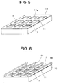
- the insulative support member 17 supports the bus electrodes 16, and prevents line failures. More specifically, as illustrated in Fig. 3, the insulative support member 17 or a material having a large electric resistance is previously formed in peripheral portions except for the electron emission devices in a thickness similar to a final thickness of the electron emission devices when formed in subsequent steps.
- the rear ribs RRs associated with the back substrate 10 is formed on the insulative support member 17 so as to protrude into the vacuum space 4 from the back substrate 10.
- the ribs RRs are positioned at predetermined intervals. While in Fig. 2, the ribs RRs are formed between respective electron emission devices S, the ribs RRs may be formed at larger intervals, for example, every two or three electron emission devices S. Also, while in Fig. 2, the ribs RRs are continuously formed in a direction substantially perpendicular to the ohmic electrodes 11, the ribs RRs may be intermittently formed so as to leave upper areas including portions abutting to the front ramparts FRs associated with the front substrate 1, as illustrated in Fig. 19. In this way, the direction in which the bus electrodes 16 extend can be matched with fluorescent layers 3R, 3G, 3B. In any case, the ribs RR are formed between the electron emission devices S.
- each of the ribs RRs has its top surface area larger than the bottom surface area which is in contact with the back substrate 10.
- each of the ribs RR is preferably formed to have an overhung portion on its top which protrudes in a direction substantially parallel with the back substrate 10.
- the bus electrodes 16 disposed on the thin-film metal electrodes 15 of the back substrate 10 are formed in a simple linear shape
- the bus electrodes 16 are preferably formed, instead of the linear shape, so as to have a width of 300 ⁇ m, by way of example, between the thin-film metal electrodes 15 of the electron emission devices larger than the width of 20 ⁇ m, by way of example, on the thin-film metal electrodes, as illustrated in Fig. 17.
- the bus electrodes 16 are preferably formed to be wider between the electron emission devices than on the devices. In this way, the resistance of the bus electrodes can be reduced. Further, as illustrated in Figs.
- the bus electrodes 16 may be formed such that they are conformal to the edges of the thin-film metal electrodes 15 by increasing the width between the thin-film metal electrodes 15 of the electron emission devices S and reducing the width on the thin-film metal electrodes (Fig. 18A), or such that they meander along the edges of the thin-film metal electrodes (Fig. 18B).
- the material for the ohmic electrodes 11 is Au, Pt, Al, W or the like which is generally used for the wires of an IC, and also a three-layered structure of chromium, nickel and chromium films, an Al and Nd alloy, an Al and Mo alloy, and, an Ti and N alloy may be used for the ohmic electrode.
- the uniform thickness of for the ohmic electrode is set for supplying substantially the same current to the individual emission devices.
- an auxiliary insulator layer comprised of an insulator such as SiO 2 , SiN x , Al 2 O 3 or AlN may be provided between the back substrate 10 and the ohmic electrode 11, but not shown in Fig. 2.
- the auxiliary insulator layer serves to prevent an adverse influence of the back substrate 10 on the device (such as elution of an impurity such as an alkaline component or a roughened substrate surface).
- the material for the thin-film metal electrode 15 has a lower work function ⁇ and is thinner.
- the material for the thin-film metal electrode 15 should be a metal of the group I or group II in the periodic table; for example, Cs, Rb, Li, Sr, Mg, Ba, Ca and the like are effective and alloys of those elements may be used as well.
- the material for the thin-film metal electrode 15 should be chemically stable with a high conductivity; for example, single substances of Au, Pt, Lu, Ag, Cu and Ir or an alloy thereof or a multi-layer thereof are desirable. It is effective to coat or dope a metal with a low work function as described above on or in those metals.
- the material for the bus electrodes 16 can be Au, Pt, Al or the like which is generally used for the wiring of an integrated circuit IC, and should have a thickness enough to supply substantially the same potential to the individual devices, adequately of 0.1 to 50 ⁇ m. If the electrical resistance of material of the thin-film metal electrode is allowable for the bus electrodes, such electrode material may be used for the bus electrodes.
- transparent collector electrodes 2 made of ITO to which a high voltage is applied are integrally formed on the inner surface (surface opposing to the back substrate 10) of the optically transparent front substrate 1 made of transparent glass and serving as a display surface.
- a black stripe mask or back metal layer is provided on the front substrate 1, such a conductive layer may be serve as a collector electrode instead of the ITO transparent collector electrode.
- a plurality of front ribs (second insulative rib) FRs are formed in parallel with the ohmic electrodes 11.
- fluorescent material layers 3R, 3G, 3B made of fluorescent materials corresponding to R, G, B are formed, respectively, in opposition to the vacuum space 4.
- the front ribs (second insulative rib) FRs are provided at boundaries of the respective fluorescent materials to maintain a constant distance (for example, 1 mm) between the back substrate and the front substrate.
- front ribs (second insulative rib) FRs are disposed on the front substrate 1 in a direction orthogonal to the rear ribs (first insulative rib) RRs disposed on the back substrate 10, it is ensured that the front substrate are definitely colored by the fluorescent materials in R, G, B corresponding to the three primary colors of light.
- the electron emission device based flat panel display apparatus has an image display array composed of a plurality of light emitting pixels which are arranged in a matrix form and each of which includes red (R), green (G) and blue (B) light emitting elements.
- a monochrome display panel may be formed by replacing all the RGB light emitting elements with monochrome light emitting elements.
- a plurality of ohmic electrodes 11 are formed on an insulating substrate such as glass or the like in stripes parallel with each other by a patterning step.
- Any material may be used for the ohmic electrodes as long as it has a small electric resistance and can be formed as a film.
- aluminum, tungsten, Cr, Cu and a multi-layer of Cu are particularly preferred.
- each of the stripes has a width of 160 ⁇ m, a thickness of 0.3 ⁇ m and a line interval of 300 ⁇ m.
- the stripe-like ohmic electrodes 11 may be formed, for example, by a method of forming films only on areas of the ohmic electrodes using an appropriate mask, or by a method of forming an electrode film over the entire surface of the substrate and then maintaining the areas of the ohmic electrodes by a variety of etching techniques. Alternatively, a screen printing method or a photo-sensitive paste method may also be employed.
- an insulative support member 17 made of an electrically insulating material is formed on the fabricated ohmic electrode surface. Portions of the insulative support member 17 are removed to have openings 17a in which electron emission devices are fabricated in subsequent steps.
- a material suitable for the insulative support member 17 is, for example, polyimide.
- the openings 17a expose the ohmic electrodes 11.
- the insulative support member 17 is formed to finally have a thickness substantially equal to the thickness of the electron emission devices, for example, 5 ⁇ m in this embodiment.
- Each of the openings 17a in which an electron emission device is subsequently fabricated, has a width of 200 ⁇ m which is larger than that of the electron emission device and a longitudinal length of 440 ⁇ m.
- Steps subsequent to the insulative support member fabricating step involve formation of a silicon film in a thickness of 5 ⁇ m as a material for an electron-supply layer for each electron emission device, and finally formation of a thin-film metal electrodes electrically continuous in a direction orthogonal to the extending direction of the metal ohmic electrodes, or formation of bus electrodes to electrically connect insular thin-film metal electrodes.
- the insulative support member 17 were not provided except for the areas left for the electron emission devices in the insulative support member fabricating step, a difference in thickness of 5- ⁇ m silicon layer serving as the electron-supply layer would cause breakage of the topmost continuous thin-film metal electrodes or the bus electrodes with a much higher probability. Even with a line failure at one location, an entire line associated with the failure would become defective in a display panel.
- the insulative support member 17 does eliminate this structural defect.
- the insulative support member 17 may be formed, for example, by using a screen printing method.
- the formation of the insulative support member 17 is included in this step because subsequent steps are free from the influence of heat required to form the insulative support member 17. Unwanted influence of heat on the devices is eliminated by performing a step requiring a thermal treatment prior to the fabrication of the devices.
- each of the rear ribs RRs formed on the insulative support member 17 between electron emission devices has a width of 100 ⁇ m and a height (thickness) of 10 ⁇ m, by way of example.
- the rear ribs RRs may also be formed, for example, by using a screen printing method.
- the back substrate It is impossible to fabricate the back substrate with ribs continuously extending in the same direction as the ohmic electrodes 11 due to possible breakage of the thin-film metal electrodes. If the back substrate was aligned to the front substrate only with the front ribs FRs interposed therebetween, the front ribs RFs of 1mm high would come in direct contact with the thin-film metal electrodes to cause breakage of the thin-film metal electrodes on the back substrate with very high probability, although no problem would arise in view of the arrangement.
- the bus electrodes could not be broken since the front ribs FRs on the front substrate abut to the rear ribs RRs on the back substrate.
- the ribs are fabricated on both the back substrate and the front substrate, the respective ribs require lower heights, thereby producing effects of facilitating the fabrication as well as increasing the structural strength after the substrates are aligned.
- the entire space is continuous by virtue of the orthogonally arranged front ribs FRs and rear ribs RRs, so that the evacuation can be effectively facilitated.
- the rear ribs RRs may be rectangular in cross section
- the rear ribs RRs preferably have a trapezoidal cross-section in the electrode direction such that the length of an area (bottom surface) contacting with the insulative support member 17 in the electrode direction is shorter than that of the top surface.
- overhung portions 18 protruding in a direction parallel with the substrate are formed on the top of the rear ribs RRs in the direction in which the rear ribs RRs extend.
- the overhung portions 18 may be formed as undercuts of the rear ribs RRs using other appropriate techniques such as a photolithographic method or the like.
- Photo-insensitive polyimide an example of a material for the ribs
- Photo-insensitive polyimide is formed on the ohmic electrodes 11 on the back substrate in a predetermined thickness, for example, by a spin coating method, and a photo resist mask made of a photo resist material is formed on the polyimide film which is then etched into the pattern of the rear ribs RRs using an appropriate technique such as reactive ion etching or the like.
- an alkaline solution serving as an etchant
- polyimide so far referred to in this specification includes precursor materials before they are imidized, and true polyimide is fabricated by curing such material in a post bake at temperatures of approximately 300°C.
- any suitable materials may be used in place of polyimide as long as they are insulating materials which do not etch the underlying support material. It is therefore possible to employ an electrically insulating material which can maintain the strength before the formation of a material film which subsequently serves as the electron-supply layers.
- silicon is deposited as a material for the electron-supply layers on each of exposed portion of the ohmic electrodes 11 through a mask 31 to form at least one electron-supply layer 12.
- the insulative support member 17 is formed with openings in which electron emission devices are fabricated.
- the mask 31 also has similar openings.
- a silicon film is formed in each of the openings of the insulative support member 17 to have a width of 240 ⁇ m, a longitudinal length of 480 ⁇ m, and a thickness of 5 ⁇ m.
- the height of the silicon layer 12 substantially matches the height of the insulative support member 17, so that no difference in level is created.
- the silicon layer 12 may be formed by any one of the vapor deposition, the sputtering method or the CVD method.
- thin-film metal electrodes 15 are formed on the insulator layer 13 separately for individual electron emission devices.
- the thin-film metal electrodes 15 may be continuously formed instead of separately formed for individual electron emission devices, provided that they are oriented in a direction orthogonal to the ohmic electrodes.
- the continuous electrodes would require a mask machined in continuous stripes as mentioned above. Such a mask having a large number of slits in stripes is difficult to handle in view of its strength reduced by the slits.
- the thin-film metal electrodes 15 are formed separately for individual electron emission devices using a mask 32 in a manner similar to the formation of the silicon electron-supply layer 12. Consequently, as illustrated in Fig. 10, the thin-film metal electrodes 15 are formed as individual insular electrodes which should be linked by bus electrodes.
- the mask 32 having openings corresponding to respective electron emission devices more reliably ensure its strength than a mask having a large number of slits in stripes.
- thin-film metal electrodes can be formed in continuous stripes, or if thin-film metal electrodes can be formed in stripes by other suitable forming methods such as etching and so on, it is not necessary to particularly insist on the formation of separate thin-film metal electrodes for individual electron emission devices using a mask.
- a suitable material for the thin-film metal electrodes may be any one having a low work function, and platinum or gold is particularly preferred.
- the thin-film metal electrodes are formed in a thickness of approximately 10 nm, and preferably formed by vapor deposition or sputtering. Alternatively, an etching method may also be employed as mentioned above.
- bus electrodes 16 are formed on portions of the thin-film metal electrodes 15 using a mask 33 by a vapor deposition method, a sputtering method or the like.
- the bus electrodes 16 are provided for ensuring conduction between the thin-film metal electrodes. While a suitable material for the bus electrodes 16 may be any one having a low electric resistance, a metal having a low resistivity such as Al, Cu, Au or the like is of course desirable.
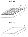
- the bus electrodes 16 provide conducting paths in a direction orthogonal to the ohmic electrodes 11, they may be linearly routed in that direction, as illustrated in Fig. 12. However, in order to ensure the conduction and reduce the resistance, the bus electrodes 16 are made narrower on the thin-film metal electrodes 15 and wider between the thin-film metal electrodes 15 to ensure a higher aperture ratio on the thin-film metal electrodes 15. For example, as illustrated in Fig. 17, the bus electrodes 16 may have a width of 300 ⁇ m between the thin-film metal electrodes 15 of the electron emission devices and a width of 20 ⁇ m on the thin-film metal electrodes 15.
- a transparent collector electrode 2 is formed over an optically transparent substrate 1 made of glass or the like.
- the transparent collector electrode 2 preferably has a high transparency for visible light and a low electric resistance, and ITO is particularly suitable for the transparent collector electrode 2.
- the transparent collector electrode 2 is formed over the entire surface of the front substrate in a thickness of 0.4 ⁇ m.
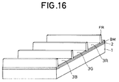
- a black matrix BM are formed on the transparent collector electrode 2.
- the black matrix BM includes openings 19 in areas corresponding to electron emission devices on the back substrate when the front substrate is aligned with the back substrate, and a light absorbent material is formed in lattice on portions other than the openings 19.
- the black matrix BM may have vertical and horizontal widths of 100 ⁇ m, respectively, and a thickness of 1 ⁇ m, and may be formed of CdTe by screen printing.
- front ribs (second insulative rib) FRs are formed on the front substrate 1 so as to be parallel with the ohmic electrodes when the front substrate is aligned with the back substrate.
- the front ribs RFs may have a width of approximately 100 ⁇ m and a height of 1 mm.
- An insulating material is used for the front ribs FRs.
- the front ribs FRs may be formed by a sand blast method which uniformly forms an insulating material over the black matrix BM in a thickness of 1 mm and blasts fine solid particles onto the insulating material, or by any suitable method such as screen printing which can provide thick films.
- This front ramparts ensure a spacing between the substrates to prevent short-circuiting between the collector electrodes and the bus electrodes, and allows vacuum spaces of a plurality of electron emission devices to communicate with each other.
- the front ribs (second insulative rib) FRs have an effect of creating a distance between the back substrate and the front substrate and an effect of serving as separator ribs when fluorescent materials are applied in a subsequent step.
- fluorescent materials 3R, 3G, 3B are alternately applied between the respective front ribs FRs.
- those used for CRT may be applied in a thickness of approximately 20 ⁇ m.
- the back substrate and the front substrate are aligned such that the ribs RR on the back substrate 10 abut to the front ramparts RFs on the front substrate 1 and both the substrates oppose to each other with the vacuum space 4 interposed therebetween, and encapsulated around the periphery of the substrates. After evacuating the space between the two substrates, getter provided inside is scattered by inductive heating, and finally, an exhaust port is sealed. This is because impurity gas produced after the encapsulation is adsorbed.
- the ohmic electrodes and the bus electrodes on the back substrate are connected to the ground and a positive voltage, respectively, while the transparent electrodes on the front substrate are connected to a positive voltage of several kV, thereby completing a flat panel display apparatus comprising a pair of optically transparent front substrate 1 and back substrate 10, as illustrated in Fig. 2.
Landscapes
- Engineering & Computer Science (AREA)
- Chemical & Material Sciences (AREA)
- Nanotechnology (AREA)
- Physics & Mathematics (AREA)
- Mathematical Physics (AREA)
- Theoretical Computer Science (AREA)
- Crystallography & Structural Chemistry (AREA)
- Cathode-Ray Tubes And Fluorescent Screens For Display (AREA)
Applications Claiming Priority (8)
| Application Number | Priority Date | Filing Date | Title |
|---|---|---|---|
| JP35846797A JPH11185678A (ja) | 1997-12-25 | 1997-12-25 | 電子放出素子フラットパネルディスプレイ装置 |
| JP35846597 | 1997-12-25 | ||
| JP35846497A JPH11185675A (ja) | 1997-12-25 | 1997-12-25 | 電子放出素子フラットパネルディスプレイ装置 |
| JP35846697 | 1997-12-25 | ||
| JP35846797 | 1997-12-25 | ||
| JP35846597A JPH11185676A (ja) | 1997-12-25 | 1997-12-25 | 電子放出素子フラットパネルディスプレイ装置 |
| JP35846497 | 1997-12-25 | ||
| JP35846697A JP3488967B2 (ja) | 1997-12-25 | 1997-12-25 | 電子放出素子フラットパネルディスプレイ装置 |
Publications (2)
| Publication Number | Publication Date |
|---|---|
| EP0926698A2 true EP0926698A2 (de) | 1999-06-30 |
| EP0926698A3 EP0926698A3 (de) | 2001-10-17 |
Family
ID=27480778
Family Applications (1)
| Application Number | Title | Priority Date | Filing Date |
|---|---|---|---|
| EP98124545A Withdrawn EP0926698A3 (de) | 1997-12-25 | 1998-12-22 | Flacher Bildschirm mit Elektronenemittern |
Country Status (2)
| Country | Link |
|---|---|
| US (1) | US6259198B1 (de) |
| EP (1) | EP0926698A3 (de) |
Cited By (1)
| Publication number | Priority date | Publication date | Assignee | Title |
|---|---|---|---|---|
| CN109041288A (zh) * | 2018-09-25 | 2018-12-18 | 佛山市昂达电器有限公司 | 一种远红外发射器件、阵列及制备方法 |
Families Citing this family (19)
| Publication number | Priority date | Publication date | Assignee | Title |
|---|---|---|---|---|
| JP2000057935A (ja) * | 1998-08-10 | 2000-02-25 | Pioneer Electron Corp | 電子放出発光素子及びこれを用いた表示装置 |
| KR100334017B1 (ko) * | 1999-03-18 | 2002-04-26 | 김순택 | 평판 디스플레이 |
| US6394870B1 (en) * | 1999-08-24 | 2002-05-28 | Eastman Kodak Company | Forming a display having conductive image areas over a light modulating layer |
| JP3688970B2 (ja) * | 2000-02-29 | 2005-08-31 | 株式会社日立製作所 | 薄膜型電子源を用いた表示装置及びその製造方法 |
| JP4323679B2 (ja) * | 2000-05-08 | 2009-09-02 | キヤノン株式会社 | 電子源形成用基板及び画像表示装置 |
| KR100741898B1 (ko) * | 2000-12-22 | 2007-07-24 | 엘지.필립스 엘시디 주식회사 | 평판형 형광램프 및 그 제조방법 |
| US7476925B2 (en) | 2001-08-30 | 2009-01-13 | Micron Technology, Inc. | Atomic layer deposition of metal oxide and/or low asymmetrical tunnel barrier interploy insulators |
| US7589029B2 (en) | 2002-05-02 | 2009-09-15 | Micron Technology, Inc. | Atomic layer deposition and conversion |
| US7160577B2 (en) | 2002-05-02 | 2007-01-09 | Micron Technology, Inc. | Methods for atomic-layer deposition of aluminum oxides in integrated circuits |
| US7192892B2 (en) | 2003-03-04 | 2007-03-20 | Micron Technology, Inc. | Atomic layer deposited dielectric layers |
| JP2004287118A (ja) * | 2003-03-24 | 2004-10-14 | Hitachi Ltd | 表示装置 |
| KR20060059616A (ko) * | 2004-11-29 | 2006-06-02 | 삼성에스디아이 주식회사 | 스페이서를 구비하는 전자방출 표시장치 |
| JP2006202523A (ja) * | 2005-01-18 | 2006-08-03 | Hitachi Displays Ltd | 画像表示装置 |
| JP2006201423A (ja) * | 2005-01-20 | 2006-08-03 | Seiko Epson Corp | 色要素付き基板、成膜方法、電気光学装置および電子機器 |
| US7687409B2 (en) | 2005-03-29 | 2010-03-30 | Micron Technology, Inc. | Atomic layer deposited titanium silicon oxide films |
| US7662729B2 (en) | 2005-04-28 | 2010-02-16 | Micron Technology, Inc. | Atomic layer deposition of a ruthenium layer to a lanthanide oxide dielectric layer |
| US7572695B2 (en) | 2005-05-27 | 2009-08-11 | Micron Technology, Inc. | Hafnium titanium oxide films |
| US7927948B2 (en) | 2005-07-20 | 2011-04-19 | Micron Technology, Inc. | Devices with nanocrystals and methods of formation |
| KR20070046670A (ko) * | 2005-10-31 | 2007-05-03 | 삼성에스디아이 주식회사 | 전자 방출 디바이스 및 이를 구비한 전자 방출 표시디바이스 |
Family Cites Families (5)
| Publication number | Priority date | Publication date | Assignee | Title |
|---|---|---|---|---|
| US5675212A (en) * | 1992-04-10 | 1997-10-07 | Candescent Technologies Corporation | Spacer structures for use in flat panel displays and methods for forming same |
| GB9216647D0 (en) * | 1992-08-05 | 1992-09-16 | Isis Innovation | Cold cathodes |
| JP3633154B2 (ja) * | 1996-03-22 | 2005-03-30 | 株式会社日立製作所 | 薄膜型電子源および薄膜型電子源応用機器 |
| JP3281533B2 (ja) * | 1996-03-26 | 2002-05-13 | パイオニア株式会社 | 冷電子放出表示装置及び半導体冷電子放出素子 |
| JPH10308165A (ja) * | 1997-03-04 | 1998-11-17 | Pioneer Electron Corp | 電子放出素子及びこれを用いた表示装置 |
-
1998
- 1998-12-22 EP EP98124545A patent/EP0926698A3/de not_active Withdrawn
- 1998-12-23 US US09/219,779 patent/US6259198B1/en not_active Expired - Fee Related
Cited By (2)
| Publication number | Priority date | Publication date | Assignee | Title |
|---|---|---|---|---|
| CN109041288A (zh) * | 2018-09-25 | 2018-12-18 | 佛山市昂达电器有限公司 | 一种远红外发射器件、阵列及制备方法 |
| CN109041288B (zh) * | 2018-09-25 | 2023-12-15 | 佛山市昂达电器有限公司 | 一种远红外发射器件、阵列及制备方法 |
Also Published As
| Publication number | Publication date |
|---|---|
| EP0926698A3 (de) | 2001-10-17 |
| US6259198B1 (en) | 2001-07-10 |
Similar Documents
| Publication | Publication Date | Title |
|---|---|---|
| JP3874396B2 (ja) | 電子放出素子及びその製造方法並びに電子放出素子を用いた表示装置 | |
| US6285123B1 (en) | Electron emission device with specific island-like regions | |
| US6259198B1 (en) | Flat panel display apparatus with an array of electron emitting devices | |
| US6787992B2 (en) | Display device of flat panel structure with emission devices of matrix array | |
| JP3698390B2 (ja) | 電子放出表示装置及び電子放出装置 | |
| EP0911854A1 (de) | Elektronenemissionsvorrichtung und Anzeigevorrichtung unter Verwendung derselben | |
| EP0863532A1 (de) | Elektronenemissionsvorrichtung und Anzeigevorrichtung unter Verwendung derselben | |
| JP3765671B2 (ja) | 電子放出素子及びこれを用いた電子放出表示装置 | |
| US6400070B1 (en) | Electron emission device and display device using the same | |
| EP0865062B1 (de) | Herstellungsverfahren einer Elektronenemissionsvorrichtung und Anzeigevorrichtung | |
| JP4253416B2 (ja) | 電子放出素子を用いた撮像素子 | |
| US6472803B1 (en) | Electron emission light-emitting device and display apparatus using the same | |
| US6700132B2 (en) | Flat panel display device utilizing electron emission devices | |
| US6278230B1 (en) | Electron emission device and display device using the same | |
| JP4676428B2 (ja) | 電子放出装置及びその製造方法並びに電子放出装置を用いた撮像装置又は表示装置 | |
| JP3461145B2 (ja) | 電子放出素子及びこれを用いた表示装置 | |
| JP3488967B2 (ja) | 電子放出素子フラットパネルディスプレイ装置 | |
| JPH11185676A (ja) | 電子放出素子フラットパネルディスプレイ装置 | |
| JP3821482B2 (ja) | 電子放出素子の製造方法 | |
| JPH11185675A (ja) | 電子放出素子フラットパネルディスプレイ装置 | |
| JPH11185678A (ja) | 電子放出素子フラットパネルディスプレイ装置 | |
| JP5026459B2 (ja) | 電子放出素子アレイおよびその製造方法 |
Legal Events
| Date | Code | Title | Description |
|---|---|---|---|
| PUAI | Public reference made under article 153(3) epc to a published international application that has entered the european phase |
Free format text: ORIGINAL CODE: 0009012 |
|
| AK | Designated contracting states |
Kind code of ref document: A2 Designated state(s): AT BE CH CY DE DK ES FI FR GB GR IE IT LI LU MC NL PT SE Kind code of ref document: A2 Designated state(s): DE FR GB |
|
| AX | Request for extension of the european patent |
Free format text: AL;LT;LV;MK;RO;SI |
|
| PUAL | Search report despatched |
Free format text: ORIGINAL CODE: 0009013 |
|
| AK | Designated contracting states |
Kind code of ref document: A3 Designated state(s): AT BE CH CY DE DK ES FI FR GB GR IE IT LI LU MC NL PT SE |
|
| AX | Request for extension of the european patent |
Free format text: AL;LT;LV;MK;RO;SI |
|
| RIC1 | Information provided on ipc code assigned before grant |
Free format text: 7H 01J 31/12 A, 7H 01J 1/312 B |
|
| 17P | Request for examination filed |
Effective date: 20020130 |
|
| AKX | Designation fees paid |
Free format text: DE FR GB |
|
| 17Q | First examination report despatched |
Effective date: 20070820 |
|
| STAA | Information on the status of an ep patent application or granted ep patent |
Free format text: STATUS: THE APPLICATION IS DEEMED TO BE WITHDRAWN |
|
| 18D | Application deemed to be withdrawn |
Effective date: 20080301 |