EP0926738A2 - Festkörper-Bildaufnahmevorrichtung - Google Patents
Festkörper-Bildaufnahmevorrichtung Download PDFInfo
- Publication number
- EP0926738A2 EP0926738A2 EP98310660A EP98310660A EP0926738A2 EP 0926738 A2 EP0926738 A2 EP 0926738A2 EP 98310660 A EP98310660 A EP 98310660A EP 98310660 A EP98310660 A EP 98310660A EP 0926738 A2 EP0926738 A2 EP 0926738A2
- Authority
- EP
- European Patent Office
- Prior art keywords
- photoelectric conversion
- charge transfer
- transfer means
- conversion portion
- signal
- Prior art date
- Legal status (The legal status is an assumption and is not a legal conclusion. Google has not performed a legal analysis and makes no representation as to the accuracy of the status listed.)
- Ceased
Links
- 238000006243 chemical reaction Methods 0.000 claims abstract description 57
- 238000003491 array Methods 0.000 claims 1
- 238000009792 diffusion process Methods 0.000 description 27
- 101100422768 Saccharomyces cerevisiae (strain ATCC 204508 / S288c) SUL2 gene Proteins 0.000 description 9
- 101100194363 Schizosaccharomyces pombe (strain 972 / ATCC 24843) res2 gene Proteins 0.000 description 9
- XAGFODPZIPBFFR-UHFFFAOYSA-N aluminium Chemical compound [Al] XAGFODPZIPBFFR-UHFFFAOYSA-N 0.000 description 6
- 229910052782 aluminium Inorganic materials 0.000 description 6
- 238000012986 modification Methods 0.000 description 5
- 230000004048 modification Effects 0.000 description 5
- 230000035945 sensitivity Effects 0.000 description 4
- 238000004891 communication Methods 0.000 description 2
- 230000003287 optical effect Effects 0.000 description 2
- 229910021420 polycrystalline silicon Inorganic materials 0.000 description 2
- 229920005591 polysilicon Polymers 0.000 description 2
- 230000003247 decreasing effect Effects 0.000 description 1
- 238000003384 imaging method Methods 0.000 description 1
- 230000010354 integration Effects 0.000 description 1
Images







Classifications
-
- H—ELECTRICITY
- H10—SEMICONDUCTOR DEVICES; ELECTRIC SOLID-STATE DEVICES NOT OTHERWISE PROVIDED FOR
- H10F—INORGANIC SEMICONDUCTOR DEVICES SENSITIVE TO INFRARED RADIATION, LIGHT, ELECTROMAGNETIC RADIATION OF SHORTER WAVELENGTH OR CORPUSCULAR RADIATION
- H10F39/00—Integrated devices, or assemblies of multiple devices, comprising at least one element covered by group H10F30/00, e.g. radiation detectors comprising photodiode arrays
- H10F39/80—Constructional details of image sensors
- H10F39/802—Geometry or disposition of elements in pixels, e.g. address-lines or gate electrodes
-
- H—ELECTRICITY
- H10—SEMICONDUCTOR DEVICES; ELECTRIC SOLID-STATE DEVICES NOT OTHERWISE PROVIDED FOR
- H10F—INORGANIC SEMICONDUCTOR DEVICES SENSITIVE TO INFRARED RADIATION, LIGHT, ELECTROMAGNETIC RADIATION OF SHORTER WAVELENGTH OR CORPUSCULAR RADIATION
- H10F39/00—Integrated devices, or assemblies of multiple devices, comprising at least one element covered by group H10F30/00, e.g. radiation detectors comprising photodiode arrays
- H10F39/10—Integrated devices
- H10F39/12—Image sensors
- H10F39/18—Complementary metal-oxide-semiconductor [CMOS] image sensors; Photodiode array image sensors
-
- H—ELECTRICITY
- H10—SEMICONDUCTOR DEVICES; ELECTRIC SOLID-STATE DEVICES NOT OTHERWISE PROVIDED FOR
- H10F—INORGANIC SEMICONDUCTOR DEVICES SENSITIVE TO INFRARED RADIATION, LIGHT, ELECTROMAGNETIC RADIATION OF SHORTER WAVELENGTH OR CORPUSCULAR RADIATION
- H10F39/00—Integrated devices, or assemblies of multiple devices, comprising at least one element covered by group H10F30/00, e.g. radiation detectors comprising photodiode arrays
- H10F39/80—Constructional details of image sensors
- H10F39/803—Pixels having integrated switching, control, storage or amplification elements
Definitions
- the present invention relates to a solid-state image pickup device and an image pickup system using the same and, more particularly, to a solid-state image pickup device having a plurality of photoelectric conversion portions arrayed in the row and column directions, a charge transfer means for transferring signal charges generated in the photoelectric conversion portions, and an amplifier means for amplifying a signal corresponding to the signal charges transferred by the charge transfer means and outputting the signal.
- a device of FET moving scheme is known as a MOS solid-state image pickup device.
- a solid-state image pickup device called a CMOS sensor is disclosed in Japanese Laid-Open Patent Application No. 09-46596. The arrangement will be briefly described below.
- Fig. 1 is an explanatory view showing a pixel arrangement corresponding to one pixel of a CMOS sensor disclosed in Fig. 8 of Japanese Laid-Open Patent Application No. 09-46596.
- one pixel has a photodiode portion PD, a transfer switch MS11 for transferring signal charges from the photodiode portion PD, an amplifier means MS14 for amplifying the transferred signal and outputting it, a selection switch MS13 for selecting the pixel, and a reset switch MS12 for clearing the remaining signal charges and resetting them to a potential VR.
- Signals ⁇ TX, ⁇ RES, and ⁇ SEL are used to control the transfer switch MS11, reset switch MS12, and selection switch MS13, respectively.
- a solid-state image pickup device comprising a photoelectric conversion portion, charge transfer means for transferring signal charges generated in the photoelectric conversion portion, and amplifier means for amplifying a signal corresponding to the signal charges transferred from the charge transfer means and outputting the signal, wherein a plurality of photoelectric conversion portions, a plurality of charge transfer means, and a plurality of amplifier means are arranged in row or/and column directions, and the charge transfer means and the amplifier means which are closest to each other are connected.
- a solid-state image pickup device wherein a plurality of photoelectric conversion portions are arranged in row and column directions, and charge transfer means for transferring signal charges generated in the photoelectric conversion portions are arranged in the row and column directions in correspondence with the photoelectric conversion portions, and reset means for resetting the charge transfer means or the charge transfer means and the photoelectric conversion portions corresponding to the charge transfer means are arranged on one side of an array direction of the charge transfer means, and amplifier means for amplifying a signal corresponding to the signal charges transferred from the charge transfer means are arranged on the other side of the array direction of the charge transfer means.
- a solid-state image pickup device wherein a plurality of photoelectric conversion portions are arranged in row and column directions, and charge transfer means for transferring signal charges generated in the photoelectric conversion portions and reset means for resetting the charge transfer means or the charge transfer means and the photoelectric conversion portions are arranged in one of the row and column directions around the photoelectric conversion portions, and amplifier means for amplifying a signal corresponding to the signal charges transferred from one photoelectric conversion portion and outputting the signal is arranged in the other direction different from the one direction of the one photoelectric conversion portion around which the charge transfer means and the reset means are arranged or in the other direction around another photoelectric conversion portion in a diagonal direction, the amplifier means being arranged on a side closest to the one photoelectric conversion portion.
- an image pickup system comprising a solid-state image pickup device including a photoelectric conversion portion, charge transfer means for transferring signal charges generated in the photoelectric conversion portion, and amplifier means for amplifying a signal corresponding to the signal charges transferred from the charge transfer means and outputting the signal, wherein a plurality of photoelectric conversion portions, a plurality of charge transfer means, and a plurality of amplifier means are arranged in row or/and column directions, and the charge transfer means and the amplifier means which are closest to each other are connected, and a signal processing circuit for processing the signal output from the solid-state image pickup device.
- PD photodiode portion
- TX transfer switch
- FD floating diffusion
- RE reset switch
- VR reset power source
- SEL selection switch
- SF amplifier means
- OUT output portion
- VDD VDD power source
- a VDD power source when used as a reset power source, an arrangement shown in Fig. 2 is preferably used. If the reset power source (VR) is arranged independently of the VDD power source, an arrangement shown in Fig. 3 is preferably used.
- the present invention has been made as a result of extensive studies and examinations by the present inventors to solve the above problem while maintaining the arrangement shown in Fig. 2 or 3.
- CMOS sensor using a photogate CMOS sensor using a photogate
- Fig. 10 CMOS sensor using a photodiode
- One pixel of a sensor of this type normally has an almost rectangular shape or a shape similar to a rectangle, and pixel building members including a transfer switch TX and a reset switch RES are located around the photoelectric conversion portion such as a photodiode portion PD.
- an arrangement having a photodiode portion PD2, a transfer switch TX2, a floating diffusion FD2, a reset switch RES2, a selection switch SEL2, an amplifier means SF2, and an output portion OUT2, as shown in Fig. 4, 5, 7, or 12 etc. may be regarded as one pixel, so a signal may be output from the pixel having the photodiode portion PD2 using an amplifier means SF1 or SF3 of another pixel.
- Fig. 4 is a view showing a schematic layout of the first embodiment of the present invention. This embodiment corresponds to the arrangement shown in Fig. 2 which uses a VDD power source as a reset power source.
- the floating diffusion FD2 around the photodiode portion PD2 is connected to the amplifier means SF1 on the photodiode portion PD1 side.
- the interconnection is shorter than that when the floating diffusion FD2 and the gate of the amplifier means SF2 are connected, and the interconnection does not run above the gate of the reset switch RES2 or the gate of the selection switch SEL2. Consequently, problems (1) to (3) above can be solved.
- Figs. 5 and 6 are views showing the schematic layout shown in Fig. 4 more specifically.
- Fig. 5 shows a layout without a second aluminum layer as an upper interconnection.
- Fig. 6 shows a layout including a second aluminum layer as an upper interconnection.
- Figs. 5 and 6 show only four pixels. Only a signal read from the photodiode portion PD2 will be described below, and this also applies to the remaining photodiode portions.
- the transfer switch TX2, floating diffusion FD2, reset switch RES2, selection switch SEL2, amplifier means SF2, and output portion OUT2 surround around the photodiode portion PD2.
- a VDD power source which also serves as a reset power source is interposed between the reset switch RES2 and the selection switch SEL2.
- a region indicated by a bold line in Fig. 5 is an active region.
- the signal from the photodiode portion PD2 is output not through the amplifier means SF2 and output portion OUT2 but through the amplifier means SF1 and output portion OUT1 arranged on the side of the photodiode portion PD1 arrayed on the same row.
- the floating diffusion FD2 on the photodiode portion PD2 side and the amplifier means SF1 on the photodiode portion PD1 side are connected using a polysilicon layer and a first aluminum layer.
- the amplifier means SF1 and output portion OUT1 are formed in the same active region as that of the photodiode portion PD1.
- the interconnection between the floating diffusion FD and the amplifier means SF shortens, and the interconnection is not formed above the gate of the reset switch RES or the gate of the selection switch SEL.
- the interconnection between the floating diffusion FD2 and the amplifier means SF1 runs between the control line of a signal ⁇ nSEL and the control line of a signal ⁇ nRES to prevent the output signal from being influenced by the signal ⁇ nSEL or ⁇ nRES, as shown in Fig. 6.
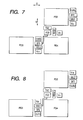
- Fig. 7 is a view showing a schematic layout of the second embodiment of the present invention. This embodiment corresponds to the arrangement shown in Fig. 3 having a reset power source independently of a VDD power source.
- a floating diffusion FD2 around the photodiode portion PD2 is connected to the amplifier means SF3 around the photodiode portion PD3.
- the photodiode portion PD has a rectangular shape.
- the photodiode portion PD need not always have this shape and can have any shape as far as the shape allows to maximize the amount of charges to be stored.
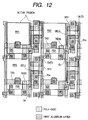
- Figs. 12 and 13 are views showing the layout in Fig. 7 more specifically.
- Fig. 12 shows a layout without a second aluminum layer as an upper interconnection.
- Fig. 13 shows a layout including a second aluminum layer as an upper interconnection.
- Figs. 12 and 13 show only four pixels. Only a signal read from the photodiode portion PD2 will be described below, and this also applies to the remaining photodiode portions.
- the transfer switch TX2, floating diffusion FD2, reset switch RES2, selection switch SEL2, amplifier means SF2, and output portion OUT2 are arranged around the photodiode portion PD2.
- a reset power source Vr and VDD power source are mounted adjacent to the reset switch RES2 and selection switch SEL2.
- Two regions indicated by bold lines in Fig. 12 are active regions.
- the signal from the photodiode portion PD2 is output not through the amplifier means SF2 and output portion OUT2 but through the amplifier means SF3 and output portion OUT3 surrounding the photodiode portion PD3 in the diagonal direction.
- the floating diffusion FD2 around the photodiode portion PD2 and the amplifier means SF3 around the photodiode portion PD3 are connected using a polysilicon layer and a first aluminum layer.
- the interconnection between the floating diffusion FD and the amplifier means SF shortens, and the interconnection does not run above the gate of the reset switch RES or the gate of the selection switch SEL.
- the gate of the selection switch SEL3 is connected to the control line of the signal ⁇ nSEL. For this reason, even when the control line of a signal ⁇ n+1SEL extends above the floating diffusion FD2, the problem of crosstalk is not posed.
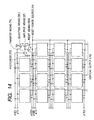
- Fig. 14 is a view showing the circuit arrangement of a pixel portion of the solid-state image pickup devices of the first and second embodiments.
- Fig. 14 shows a 4 ⁇ 4 pixel arrangement, and one pixel has the same arrangement as that shown in Fig. 1.
- a selection means may be connected between an amplifier means and an output portion, as shown in Fig. 15.
- Fig. 16 is a view showing a schematic layout of a solid-state image pickup device having the pixel arrangement shown in Fig. 15.
- a VDD power source VDD and output portion OUT are reversed to those of the layout shown in Fig. 2.
- the interconnection becomes shorter than that in connecting a floating diffusion FD2 and the gate of an amplifier means SF2, so the interconnection does not run above the gate of a reset switch RES2 and the gate of a selection switch SEL2.
- Fig. 17 is a view schematically showing, as the fourth embodiment, a solid-image pickup system using one of the solid-state image pickup devices described in the first to third embodiments.
- the image of light incident through an optical system 71 and an iris 80 is formed on a solid-state image pickup device 72.
- the light information is converted into an electrical signal by a pixel array on the solid-state image pickup device 72 and output.
- the output signal is converted by a signal processing circuit 73 on the basis of a predetermined scheme and output.
- the processed signal is recorded or transferred by an information recording device in a recording system/communication system 74.
- the recorded or transferred signal is reproduced by a reproducing system 77.
- the iris 80, solid-state image pickup device 72, and signal processing circuit 73 are controlled by a timing control circuit 75.
- the optical system 71, timing control circuit 75, recording system/communication system 74, and reproducing system 77 are controlled by a system control circuit 76.
- the interconnection between the floating diffusion (FD) and the amplifier means (SF) shortens, and the interconnection does not run above the gate of the reset means (RES) and the gate of the selection means (SEL). Since no crosstalk is generated from the signal ⁇ RES or ⁇ SEL, a solid-state image pickup device having a high fill factor and sensitivity and an image pickup system using the device can be obtained.
Landscapes
- Solid State Image Pick-Up Elements (AREA)
- Transforming Light Signals Into Electric Signals (AREA)
Priority Applications (1)
| Application Number | Priority Date | Filing Date | Title |
|---|---|---|---|
| EP07075878A EP1870937A1 (de) | 1997-12-26 | 1998-12-23 | Anordnung für Steuerleitungen in einem Bildsensor mit aktiven Pixeln |
Applications Claiming Priority (2)
| Application Number | Priority Date | Filing Date | Title |
|---|---|---|---|
| JP36108497 | 1997-12-26 | ||
| JP36108497A JP3496918B2 (ja) | 1997-12-26 | 1997-12-26 | 固体撮像装置 |
Related Child Applications (1)
| Application Number | Title | Priority Date | Filing Date |
|---|---|---|---|
| EP07075878A Division EP1870937A1 (de) | 1997-12-26 | 1998-12-23 | Anordnung für Steuerleitungen in einem Bildsensor mit aktiven Pixeln |
Publications (2)
| Publication Number | Publication Date |
|---|---|
| EP0926738A2 true EP0926738A2 (de) | 1999-06-30 |
| EP0926738A3 EP0926738A3 (de) | 2000-05-10 |
Family
ID=18472133
Family Applications (2)
| Application Number | Title | Priority Date | Filing Date |
|---|---|---|---|
| EP07075878A Withdrawn EP1870937A1 (de) | 1997-12-26 | 1998-12-23 | Anordnung für Steuerleitungen in einem Bildsensor mit aktiven Pixeln |
| EP98310660A Ceased EP0926738A3 (de) | 1997-12-26 | 1998-12-23 | Festkörper-Bildaufnahmevorrichtung |
Family Applications Before (1)
| Application Number | Title | Priority Date | Filing Date |
|---|---|---|---|
| EP07075878A Withdrawn EP1870937A1 (de) | 1997-12-26 | 1998-12-23 | Anordnung für Steuerleitungen in einem Bildsensor mit aktiven Pixeln |
Country Status (5)
| Country | Link |
|---|---|
| US (1) | US6633334B1 (de) |
| EP (2) | EP1870937A1 (de) |
| JP (1) | JP3496918B2 (de) |
| KR (1) | KR100285391B1 (de) |
| CN (1) | CN1169351C (de) |
Cited By (6)
| Publication number | Priority date | Publication date | Assignee | Title |
|---|---|---|---|---|
| EP0954032A3 (de) * | 1998-04-30 | 2000-12-27 | Canon Kabushiki Kaisha | Festkörperbildaufnahmevorrichtung und System unter Verwendung einer solchen Vorrichtung |
| DE10063094B4 (de) * | 2000-03-02 | 2008-04-24 | Magnachip Semiconductor, Ltd. | Aktive Pixelschaltung in einem CMOS-Bildsensor |
| US7436010B2 (en) | 2003-02-13 | 2008-10-14 | Matsushita Electric Industrial Co., Ltd. | Solid state imaging apparatus, method for driving the same and camera using the same |
| US7688373B2 (en) | 2003-03-07 | 2010-03-30 | Panasonic Corporation | Solid-state imaging device with specific contact arrangement |
| US7700950B2 (en) | 2005-06-15 | 2010-04-20 | Jaroslav Hynecek | Image sensor with compact pixel layout |
| CN109979952A (zh) * | 2015-02-16 | 2019-07-05 | 佳能株式会社 | 成像设备 |
Families Citing this family (32)
| Publication number | Priority date | Publication date | Assignee | Title |
|---|---|---|---|---|
| JP4006075B2 (ja) * | 1998-01-30 | 2007-11-14 | キヤノン株式会社 | Cmosセンサ及び撮像システム |
| JP4200545B2 (ja) * | 1998-06-08 | 2008-12-24 | ソニー株式会社 | 固体撮像素子およびその駆動方法、並びにカメラシステム |
| EP0999698B1 (de) * | 1998-11-02 | 2013-06-19 | Canon Kabushiki Kaisha | Festkörper-Bildaufnahmevorrichtung und entsprechendes Resetverfahren |
| US6850278B1 (en) * | 1998-11-27 | 2005-02-01 | Canon Kabushiki Kaisha | Solid-state image pickup apparatus |
| US7324144B1 (en) * | 1999-10-05 | 2008-01-29 | Canon Kabushiki Kaisha | Solid image pickup device, image pickup system and method of driving solid image pickup device |
| US6995800B2 (en) * | 2000-01-27 | 2006-02-07 | Canon Kabushiki Kaisha | Image pickup apparatus utilizing a plurality of converging lenses |
| US7057656B2 (en) * | 2000-02-11 | 2006-06-06 | Hyundai Electronics Industries Co., Ltd. | Pixel for CMOS image sensor having a select shape for low pixel crosstalk |
| US6965408B2 (en) * | 2000-02-28 | 2005-11-15 | Canon Kabushiki Kaisha | Solid-state image pickup device having a photoelectric conversion unit and a punch-through current suppression circuit |
| JP3667214B2 (ja) | 2000-08-25 | 2005-07-06 | キヤノン株式会社 | 固体撮像装置およびその駆動方法 |
| JP3880345B2 (ja) * | 2001-08-27 | 2007-02-14 | キヤノン株式会社 | 差動増幅回路及びそれを用いた固体撮像装置並びに撮像システム |
| JP4726176B2 (ja) * | 2002-09-20 | 2011-07-20 | キヤノン株式会社 | 固体撮像装置 |
| JP3641260B2 (ja) * | 2002-09-26 | 2005-04-20 | 株式会社東芝 | 固体撮像装置 |
| JP4154268B2 (ja) * | 2003-03-27 | 2008-09-24 | キヤノン株式会社 | 撮像装置 |
| KR100523672B1 (ko) * | 2003-04-30 | 2005-10-24 | 매그나칩 반도체 유한회사 | 다중 플로팅디퓨젼영역을 구비하는 씨모스 이미지센서 |
| CN1574370A (zh) * | 2003-05-30 | 2005-02-02 | 松下电器产业株式会社 | 固体摄像器件 |
| JP4018644B2 (ja) * | 2004-01-29 | 2007-12-05 | キヤノン株式会社 | 光電変換装置及び同光電変換装置を用いた撮像システム |
| RU2352080C2 (ru) * | 2004-06-09 | 2009-04-10 | Вайа Текнолоджиз, Инк. | Способ работы модуля формирования сигнала изображения и устройство для его осуществления |
| WO2006025079A1 (ja) * | 2004-07-20 | 2006-03-09 | Fujitsu Limited | Cmos撮像素子 |
| JP4971586B2 (ja) * | 2004-09-01 | 2012-07-11 | キヤノン株式会社 | 固体撮像装置 |
| US20060113460A1 (en) * | 2004-11-05 | 2006-06-01 | Tay Hiok N | Image sensor with optimized wire routing |
| KR100690880B1 (ko) * | 2004-12-16 | 2007-03-09 | 삼성전자주식회사 | 픽셀별 광감도가 균일한 이미지 센서 및 그 제조 방법 |
| KR100680469B1 (ko) | 2005-01-31 | 2007-02-08 | 매그나칩 반도체 유한회사 | 인접한 화소들 사이의 센싱노드들이 공유된 씨모스 이미지센서 |
| KR100598015B1 (ko) | 2005-02-07 | 2006-07-06 | 삼성전자주식회사 | 공유 구조 상보성 금속 산화막 반도체 액티브 픽셀 센서어레이의 레이 아웃 |
| ZA200605213B (en) * | 2005-06-24 | 2007-09-26 | J Lok Co | Device for forming partitioned film packages |
| JP4752447B2 (ja) * | 2005-10-21 | 2011-08-17 | ソニー株式会社 | 固体撮像装置およびカメラ |
| JP4144892B2 (ja) * | 2006-08-28 | 2008-09-03 | キヤノン株式会社 | 光電変換装置及び撮像装置 |
| KR100849825B1 (ko) * | 2007-03-14 | 2008-07-31 | 동부일렉트로닉스 주식회사 | 이미지센서 및 그 제조방법 |
| JP5130946B2 (ja) * | 2008-02-15 | 2013-01-30 | ソニー株式会社 | 固体撮像装置、カメラ及び電子機器 |
| JP2009296016A (ja) * | 2009-09-18 | 2009-12-17 | Renesas Technology Corp | 固体撮像素子 |
| US9526468B2 (en) * | 2014-09-09 | 2016-12-27 | General Electric Company | Multiple frame acquisition for exposure control in X-ray medical imagers |
| JP2016111425A (ja) * | 2014-12-03 | 2016-06-20 | ルネサスエレクトロニクス株式会社 | 撮像装置 |
| JP2023063943A (ja) * | 2021-10-25 | 2023-05-10 | ソニーセミコンダクタソリューションズ株式会社 | 撮像装置 |
Family Cites Families (15)
| Publication number | Priority date | Publication date | Assignee | Title |
|---|---|---|---|---|
| USRE34309E (en) | 1984-12-26 | 1993-07-13 | Canon Kabushiki Kaisha | Image sensor device having plural photoelectric converting elements |
| US4835404A (en) | 1986-09-19 | 1989-05-30 | Canon Kabushiki Kaisha | Photoelectric converting apparatus with a switching circuit and a resetting circuit for reading and resetting a plurality of lines sensors |
| JPH07120767B2 (ja) | 1986-09-19 | 1995-12-20 | キヤノン株式会社 | 光電変換装置 |
| EP0272152B1 (de) | 1986-12-18 | 1994-08-03 | Canon Kabushiki Kaisha | Signalausleseschaltung |
| US4879470A (en) | 1987-01-16 | 1989-11-07 | Canon Kabushiki Kaisha | Photoelectric converting apparatus having carrier eliminating means |
| US5262870A (en) | 1989-02-10 | 1993-11-16 | Canon Kabushiki Kaisha | Image sensor in which reading and resetting are simultaneously performed |
| US5162912A (en) | 1989-04-10 | 1992-11-10 | Canon Kabushiki Kaisha | Photoelectric conversion apparatus eliminating noise in an output signal |
| US5184006A (en) | 1990-04-23 | 1993-02-02 | Canon Kabushiki Kaisha | Photoelectric conversion apparatus having clock signals of different frequencies |
| JPH06339082A (ja) | 1993-05-28 | 1994-12-06 | Canon Inc | 光電変換装置 |
| JP3431995B2 (ja) | 1993-06-03 | 2003-07-28 | キヤノン株式会社 | 撮像装置 |
| JP3571770B2 (ja) | 1994-09-16 | 2004-09-29 | キヤノン株式会社 | 光電変換装置 |
| JP3031606B2 (ja) * | 1995-08-02 | 2000-04-10 | キヤノン株式会社 | 固体撮像装置と画像撮像装置 |
| JPH09215001A (ja) * | 1996-02-08 | 1997-08-15 | Hitachi Ltd | 撮像装置 |
| US6160281A (en) * | 1997-02-28 | 2000-12-12 | Eastman Kodak Company | Active pixel sensor with inter-pixel function sharing |
| US6107655A (en) * | 1997-08-15 | 2000-08-22 | Eastman Kodak Company | Active pixel image sensor with shared amplifier read-out |
-
1997
- 1997-12-26 JP JP36108497A patent/JP3496918B2/ja not_active Expired - Fee Related
-
1998
- 1998-12-18 US US09/215,195 patent/US6633334B1/en not_active Expired - Fee Related
- 1998-12-23 EP EP07075878A patent/EP1870937A1/de not_active Withdrawn
- 1998-12-23 EP EP98310660A patent/EP0926738A3/de not_active Ceased
- 1998-12-24 KR KR1019980058682A patent/KR100285391B1/ko not_active Expired - Fee Related
- 1998-12-25 CN CNB981254446A patent/CN1169351C/zh not_active Expired - Fee Related
Non-Patent Citations (2)
| Title |
|---|
| MABUCHI K ET AL: "A 5.5MUM CMOS IMAGE SENSOR CELL UTILIZING A BURIED RESET CHANNEL", 1997 SYMPOSIUM ON VLSI TECHNOLOGY. DIGEST OF TECHNICAL PAPERS. KYOTO, JUNE 10 - 12, 1997, SYMPOSIUM ON VLSI TECHNOLOGY. DIGEST OF TECHNICAL PAPERS, 10 June 1997 (1997-06-10), NEW-YORK, US : IEEE, US, pages 75 - 76, XP002385578 * |
| WONG, H.-S.: "Technology and Device Scaling Considerations for CMOS Imagers", IEEE TRANSACTIONS ON ELECTRON DEVICES, IEEE SERVICE CENTER, PISACATAWAY, NJ, US, vol. 43, no. 12, December 1996 (1996-12-01), pages 2131 - 2142, XP011016027 * |
Cited By (24)
| Publication number | Priority date | Publication date | Assignee | Title |
|---|---|---|---|---|
| US6977684B1 (en) | 1998-04-30 | 2005-12-20 | Canon Kabushiki Kaisha | Arrangement of circuits in pixels, each circuit shared by a plurality of pixels, in image sensing apparatus |
| US7663680B2 (en) | 1998-04-30 | 2010-02-16 | Canon Kabushiki Kaisha | Arrangement of circuits in pixels, each circuit shared by a plurality of pixels, in image sensing apparatus |
| US9123610B2 (en) | 1998-04-30 | 2015-09-01 | Canon Kabushiki Kaisha | Arrangement of circuits in pixels, each circuit shared by a plurality of pixels, in image sensing apparatus |
| EP0954032A3 (de) * | 1998-04-30 | 2000-12-27 | Canon Kabushiki Kaisha | Festkörperbildaufnahmevorrichtung und System unter Verwendung einer solchen Vorrichtung |
| US8836834B2 (en) | 1998-04-30 | 2014-09-16 | Canon Kabushiki Kaisha | Arangement of circuits in pixels, each circuit shared by a plurality of pixels, in image sensing appratus |
| US8614757B2 (en) | 1998-04-30 | 2013-12-24 | Canon Kabushiki Kaisha | Arrangement of circuits in pixels, each circuit shared by a plurality of pixels, in image sensing apparatus |
| US8115844B2 (en) | 1998-04-30 | 2012-02-14 | Canon Kabushiki Kaisha | Arrangement of circuits in pixels, each circuit shared by a plurality of pixels, in image sensing apparatus |
| DE10063094B4 (de) * | 2000-03-02 | 2008-04-24 | Magnachip Semiconductor, Ltd. | Aktive Pixelschaltung in einem CMOS-Bildsensor |
| US8084796B2 (en) | 2003-02-13 | 2011-12-27 | Panasonic Corporation | Solid state imaging apparatus, method for driving the same and camera using the same |
| US7436010B2 (en) | 2003-02-13 | 2008-10-14 | Matsushita Electric Industrial Co., Ltd. | Solid state imaging apparatus, method for driving the same and camera using the same |
| US8378401B2 (en) | 2003-02-13 | 2013-02-19 | Panasonic Corporation | Solid state imaging apparatus, method for driving the same and camera using the same |
| US8106431B2 (en) | 2003-02-13 | 2012-01-31 | Panasonic Corporation | Solid state imaging apparatus, method for driving the same and camera using the same |
| US7696543B2 (en) | 2003-03-07 | 2010-04-13 | Panasonic Corporation | Solid-state imaging device |
| US8017983B2 (en) | 2003-03-07 | 2011-09-13 | Panasonic Corporation | Solid-state imaging device |
| US8299512B2 (en) | 2003-03-07 | 2012-10-30 | Panasonic Corporation | Solid-state imaging device |
| US8004026B2 (en) | 2003-03-07 | 2011-08-23 | Panasonic Corporation | Solid-state imaging device |
| US8592880B2 (en) | 2003-03-07 | 2013-11-26 | Panasonic Corporation | Solid-state imaging device |
| US7944493B2 (en) | 2003-03-07 | 2011-05-17 | Panasonic Corporation | Solid-state imaging device with specific contact arrangement |
| US7688373B2 (en) | 2003-03-07 | 2010-03-30 | Panasonic Corporation | Solid-state imaging device with specific contact arrangement |
| US8044446B2 (en) | 2005-06-15 | 2011-10-25 | Intellectual Ventures Ii Llc | Image sensor with compact pixel layout |
| US8217437B2 (en) | 2005-06-15 | 2012-07-10 | Intellectual Ventures Ii Llc | Image sensor with compact pixel layout |
| US7700950B2 (en) | 2005-06-15 | 2010-04-20 | Jaroslav Hynecek | Image sensor with compact pixel layout |
| CN109979952A (zh) * | 2015-02-16 | 2019-07-05 | 佳能株式会社 | 成像设备 |
| CN109979952B (zh) * | 2015-02-16 | 2023-06-30 | 佳能株式会社 | 成像设备 |
Also Published As
| Publication number | Publication date |
|---|---|
| US6633334B1 (en) | 2003-10-14 |
| EP0926738A3 (de) | 2000-05-10 |
| EP1870937A1 (de) | 2007-12-26 |
| CN1224971A (zh) | 1999-08-04 |
| JP3496918B2 (ja) | 2004-02-16 |
| KR19990063473A (ko) | 1999-07-26 |
| JPH11195776A (ja) | 1999-07-21 |
| KR100285391B1 (ko) | 2001-04-02 |
| CN1169351C (zh) | 2004-09-29 |
Similar Documents
| Publication | Publication Date | Title |
|---|---|---|
| EP0926738A2 (de) | Festkörper-Bildaufnahmevorrichtung | |
| EP0862219B1 (de) | Aktiver Bildsensor, bei dem zwei benachbarte Bildelemente ein gemeinsames elektrisches integriertes Element teilen | |
| KR100331995B1 (ko) | 촬상장치에서 복수의 화소에 의해 공유되는 각 회로의 화소내의배치 | |
| JP4267095B2 (ja) | 共有された増幅器読出しを有する能動画素画像センサ | |
| EP2253017B1 (de) | Schaltungs- und fotosensorüberlappung für einen rückseitenbeleuchtungs-bildsensor | |
| US8416329B2 (en) | Image pickup device and image pickup system | |
| JP5290923B2 (ja) | 固体撮像装置および撮像装置 | |
| KR102060843B1 (ko) | 고체 촬상 소자 및 전자 기기 | |
| US7057150B2 (en) | Solid state imager with reduced number of transistors per pixel | |
| US10070079B2 (en) | High dynamic range global shutter image sensors having high shutter efficiency | |
| US20060044434A1 (en) | Image pickup apparatus and image pickup system | |
| KR20090056846A (ko) | 고체 촬상 소자 및 카메라 | |
| TW202205652A (zh) | 固體攝像裝置、固體攝像裝置的製造方法、以及電子機器 | |
| KR20160132342A (ko) | 고체 촬상 장치 및 그 구동 방법, 및 전자 기기 | |
| KR20130018545A (ko) | 주변회로를 배치해 칩 면적증대를 억제한 촬상소자, 및 촬상장치 | |
| CN110098206A (zh) | 包括具有8共享像素结构的像素块的图像传感器 | |
| KR100820520B1 (ko) | 고체촬상장치 | |
| US7910966B2 (en) | Solid state imaging device including a semiconductor substrate on which a plurality of pixel cells have been formed | |
| US20250169219A1 (en) | Image sensor | |
| JP2002050752A (ja) | 光電変換装置およびこれを用いた撮像システム | |
| JP4851164B2 (ja) | 増幅型固体撮像装置 | |
| US20070187726A1 (en) | Solid-state imaging device, method for driving the same, method for manufacturing the same, camera, and method for driving the same | |
| JPH11331491A (ja) | 固体撮像装置 | |
| US20080117322A1 (en) | Image pickup device and imaging apparatus using the same | |
| KR20000011819A (ko) | 고체촬상장치 |
Legal Events
| Date | Code | Title | Description |
|---|---|---|---|
| PUAI | Public reference made under article 153(3) epc to a published international application that has entered the european phase |
Free format text: ORIGINAL CODE: 0009012 |
|
| AK | Designated contracting states |
Kind code of ref document: A2 Designated state(s): DE FR GB IT NL |
|
| AX | Request for extension of the european patent |
Free format text: AL;LT;LV;MK;RO;SI |
|
| PUAL | Search report despatched |
Free format text: ORIGINAL CODE: 0009013 |
|
| AK | Designated contracting states |
Kind code of ref document: A3 Designated state(s): AT BE CH CY DE DK ES FI FR GB GR IE IT LI LU MC NL PT SE |
|
| AX | Request for extension of the european patent |
Free format text: AL;LT;LV;MK;RO;SI |
|
| 17P | Request for examination filed |
Effective date: 20000925 |
|
| AKX | Designation fees paid |
Free format text: DE FR GB IT NL |
|
| 17Q | First examination report despatched |
Effective date: 20040419 |
|
| 17Q | First examination report despatched |
Effective date: 20040419 |
|
| APBN | Date of receipt of notice of appeal recorded |
Free format text: ORIGINAL CODE: EPIDOSNNOA2E |
|
| APBR | Date of receipt of statement of grounds of appeal recorded |
Free format text: ORIGINAL CODE: EPIDOSNNOA3E |
|
| APAF | Appeal reference modified |
Free format text: ORIGINAL CODE: EPIDOSCREFNE |
|
| APBT | Appeal procedure closed |
Free format text: ORIGINAL CODE: EPIDOSNNOA9E |
|
| STAA | Information on the status of an ep patent application or granted ep patent |
Free format text: STATUS: THE APPLICATION HAS BEEN REFUSED |
|
| 18R | Application refused |
Effective date: 20071128 |