EP0926834A1 - Circuit diviseur programmable - Google Patents
Circuit diviseur programmable Download PDFInfo
- Publication number
- EP0926834A1 EP0926834A1 EP98310160A EP98310160A EP0926834A1 EP 0926834 A1 EP0926834 A1 EP 0926834A1 EP 98310160 A EP98310160 A EP 98310160A EP 98310160 A EP98310160 A EP 98310160A EP 0926834 A1 EP0926834 A1 EP 0926834A1
- Authority
- EP
- European Patent Office
- Prior art keywords
- output
- divide
- circuit
- input
- stage
- Prior art date
- Legal status (The legal status is an assumption and is not a legal conclusion. Google has not performed a legal analysis and makes no representation as to the accuracy of the status listed.)
- Granted
Links
- 230000000694 effects Effects 0.000 claims description 5
- 238000010586 diagram Methods 0.000 description 8
- 101100365384 Mus musculus Eefsec gene Proteins 0.000 description 4
- 230000000630 rising effect Effects 0.000 description 4
- XUIMIQQOPSSXEZ-UHFFFAOYSA-N Silicon Chemical compound [Si] XUIMIQQOPSSXEZ-UHFFFAOYSA-N 0.000 description 2
- 229910052710 silicon Inorganic materials 0.000 description 2
- 239000010703 silicon Substances 0.000 description 2
- 101100191136 Arabidopsis thaliana PCMP-A2 gene Proteins 0.000 description 1
- 101100422768 Saccharomyces cerevisiae (strain ATCC 204508 / S288c) SUL2 gene Proteins 0.000 description 1
- 101100048260 Saccharomyces cerevisiae (strain ATCC 204508 / S288c) UBX2 gene Proteins 0.000 description 1
- 238000010276 construction Methods 0.000 description 1
- 230000001419 dependent effect Effects 0.000 description 1
- 238000005516 engineering process Methods 0.000 description 1
Images




Classifications
-
- H—ELECTRICITY
- H03—ELECTRONIC CIRCUITRY
- H03L—AUTOMATIC CONTROL, STARTING, SYNCHRONISATION OR STABILISATION OF GENERATORS OF ELECTRONIC OSCILLATIONS OR PULSES
- H03L7/00—Automatic control of frequency or phase; Synchronisation
- H03L7/06—Automatic control of frequency or phase; Synchronisation using a reference signal applied to a frequency- or phase-locked loop
- H03L7/16—Indirect frequency synthesis, i.e. generating a desired one of a number of predetermined frequencies using a frequency- or phase-locked loop
- H03L7/18—Indirect frequency synthesis, i.e. generating a desired one of a number of predetermined frequencies using a frequency- or phase-locked loop using a frequency divider or counter in the loop
- H03L7/183—Indirect frequency synthesis, i.e. generating a desired one of a number of predetermined frequencies using a frequency- or phase-locked loop using a frequency divider or counter in the loop a time difference being used for locking the loop, the counter counting between fixed numbers or the frequency divider dividing by a fixed number
-
- H—ELECTRICITY
- H03—ELECTRONIC CIRCUITRY
- H03K—PULSE TECHNIQUE
- H03K23/00—Pulse counters comprising counting chains; Frequency dividers comprising counting chains
- H03K23/40—Gating or clocking signals applied to all stages, i.e. synchronous counters
- H03K23/50—Gating or clocking signals applied to all stages, i.e. synchronous counters using bi-stable regenerative trigger circuits
- H03K23/54—Ring counters, i.e. feedback shift register counters
- H03K23/544—Ring counters, i.e. feedback shift register counters with a base which is an odd number
-
- H—ELECTRICITY
- H03—ELECTRONIC CIRCUITRY
- H03K—PULSE TECHNIQUE
- H03K23/00—Pulse counters comprising counting chains; Frequency dividers comprising counting chains
- H03K23/64—Pulse counters comprising counting chains; Frequency dividers comprising counting chains with a base or radix other than a power of two
- H03K23/66—Pulse counters comprising counting chains; Frequency dividers comprising counting chains with a base or radix other than a power of two with a variable counting base, e.g. by presetting or by adding or suppressing pulses
-
- H—ELECTRICITY
- H03—ELECTRONIC CIRCUITRY
- H03K—PULSE TECHNIQUE
- H03K23/00—Pulse counters comprising counting chains; Frequency dividers comprising counting chains
- H03K23/64—Pulse counters comprising counting chains; Frequency dividers comprising counting chains with a base or radix other than a power of two
- H03K23/66—Pulse counters comprising counting chains; Frequency dividers comprising counting chains with a base or radix other than a power of two with a variable counting base, e.g. by presetting or by adding or suppressing pulses
- H03K23/667—Pulse counters comprising counting chains; Frequency dividers comprising counting chains with a base or radix other than a power of two with a variable counting base, e.g. by presetting or by adding or suppressing pulses by switching the base during a counting cycle
Definitions
- This invention relates to a programmable divider circuit which can selectively divide by predetermined odd or even integers.
- Clock divider circuits are useful in a number of applications, particularly in counters, where a complete cycle of the output signal represents a predetermined number of incoming clock cycles.
- the cycles of the output signal can be used to "count" the incoming clock cycles.
- clock divider circuits it is desirable for such clock divider circuits to work at low power and at high frequencies.
- desired operating parameters might be a current consumption of 10 ⁇ A at a supply voltage of 3.3V, with an operating frequency of around 100MHz. It is also desirable that such divider circuits consume a minimum amount of silicon when implemented on an integrated circuit.
- Existing counters are generally based on binary counters.
- the basic unit for a binary counter is a divide-by-two unit, extra logic is required to implement counts by odd numbers or even numbers which are not 2 n , where n is an integer. This extra logic reduces the highest operating frequency obtainable by the counting circuit and also consumes chip area.
- existing binary counters rarely produce an output signal which has a 50% duty cycle when dividing by odd integers.
- Signals having a 50% duty cycle are particularly desirable because in such signals there is the maximum possible time for the rising and falling edges to complete. This avoids pulse shrinkage, both in terms of amplitude and timing of the signal, which can result in duty cycles which are significantly different from 50%, and which may affect the overall timing as a result. Moreover, many circuits use both the rising and falling edges of a clock signal, so that it can be advantageous to provide the falling edge midway through the cycle of rising edges.
- a programmable dividing circuit comprising:
- the tri-state inverter stage is the last stage in the sequence and generates an output signal having a duty cycle of 50%.
- first and second circuit branches there is a common sequence of an even number x transistor stages which has an output node connected to first and second circuit branches.
- the first branch comprises q transistor stages where q is an odd integer greater than or equal to one and the second branch comprises r transistor stages and said tri-state inverter, where r is an even integer greater than or equal to zero.
- the switching circuit is a multiplexer and can be provided with a select input for receiving a programming signal to effect the selective connection.
- a single two-input multiplexer allows two different programmable options to be achieved. However, it is possible to provide a number of different dividing factors by providing one or more additional multiplexers and/or one or more additional inputs for the or each multiplexer. In this manner, a wide variety of different programming options for the dividing factor are available.
- the invention further provides a phase locked loop using a programmable dividing circuit as described herein.
- the divider circuit described herein can operate at low powers, for example drawing a current of less than 10 ⁇ A at a supply voltage of 3.3V and can operate up to high frequencies. It is envisaged that operation up to a frequency of 1GHz is possible, limited only by the characteristics of a single CMOS transistor.
- the divide-by-three circuit comprises three stages S1,S2,S3 connected in a ring which an input node of each stage connected to an output node of a preceding stage.
- Each stage comprises a first pair of p-channel MOS transistors T1,T2 and a second pair of n-channel MOS transistors T3,T4. Only the first stage S1 is described in detail herein, the remaining stages being the same.
- the transistors T1,T2 of the first pair are connected in series between a supply voltage Vdd and an output node O1.
- the transistors T3,T4 of the second pair are connected in series between the output node O1 and ground.
- the gate of the outermost transistor of each pair T1,T4 is connected to an input node I1 for the stage S1.
- the gates of the inner two transistors T2,T3 are connected to receive an input clock signal CLK IN and form a clock node for the stage.
- S2 and S3 represent similar stages, each of which has an outer set of transistors connected to an input node for the stage and an inner set of transistors connected to the input clock signal CLK IN.
- An output signal may be taken from the circuit at the output node of any of the stages, but in Figure 1 a single output CLK OUT is shown for convenience at the output of the third stage S3.
- the circuit represents a divide-by-three counter, that is, one cycle of the output signal CLK OUT represents three cycles of the input signal CLK IN.
- the circuit causes a change in state in the output signal which is dependent not only on a clock edge but also on the logical state of the data preceding the clock edge.
- the data is the signal applied to the input node of a stage from the preceding stage.
- Figure 3 represents the truth table for each stage of the divider circuit.
- stage S1 when the voltage at the input node I1 has logic stage zero, transistor T4 is off and transistor T1 is turned on.
- transistor T2 when the input signal CLK IN has a logic state of zero, transistor T2 is likewise turned on, creating a current path which allows the output node O1 to be pulled up to Vdd, as shown in the first line of the truth table of Figure 3.
- the transistor T2 is turned off with the consequence that the output node O1 "floats" at the logic state it held previously. That is, the output node represents a high impedance state to the subsequent stage and is not driving any output current.
- the transistor T1 When the voltage at the input node I1 is in logic state one, the transistor T1 is turned off and the transistor T4 is turned on. Now, with the input clock signal CLK IN at logic state zero, the transistor T3 remains off and so the output node O1 floats. When the logic state of the input signal CLK IN changes to a one, the transistor T3 is turned on to create a current path allowing the transistors T3 and T4 to pull the output node O1 down to ground.
- Initialisation is not required to start the divider circuit. It will self-start within a few cycles of the input signal as a result of small asymmetries in the layout. However, initialisation circuitry may be added if desired to force a particular initial state. It will readily be appreciated that logic circuitry such as that marked L in Figure 1 may be inserted between any two sequential stages of the ring, provided that the logic circuitry is not inverting.
- Power consumption of the circuit is very low compared with existing divider circuits.
- One reason for this is that only one internal node changes state on each clock edge, so that the power consumption is dominated by the charge/discharge currents of the capacitance of a single node.
- the maximum operating frequency of the circuit can be very high, because the delay introduced by each stage is only that introduced by a single transistor. In other words, each stage only comprises one "layer" of transistor logic requiring a change in state between input and output.
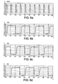
- the circuit of Figure 1 has the useful property of maintaining a duty cycle of 50% in the output signal if the input signal has a duty cycle of 50%.
- Figure 5a represents the input waveform at a duty cycle of 50%.
- Figures 5b to 5d represent the output waveforms at the nodes marked V1,V2 and V3 in Figure 1 respectively.
- the output signal of each stage when the input signal CLK IN has a duty cycle of 50%, the output signal of each stage also has a duty cycle of 50%.
- the output of each stage has a specific and predictable phase relationship with the output of other stages, providing the designer with great flexibility concerning applications of the divider circuit.
- the circuit also has the property of "improving" the duty cycle of the input signal CLK IN, where it is not 50%.
- the manner of operation of the circuit ensures that an output signal always has a duty cycle closer to 50% than the input signal. If the percentage difference from 50% of the duty cycle of the incoming signal is designated ⁇ IN , the difference ⁇ OUT from 50% of the duty cycle in the output signal is ⁇ IN divided by N where N is the number of stages in the dividing circuit. Thus, the "error" in the duty cycle is reduced by the number of stages in the dividing circuit ring.
- An example of this is shown for the divide-by-three circuit in Figure 1 in the waveforms of Figures 6a to 6d.
- Figure 6a represents the input signal having a duty cycle of 20%.
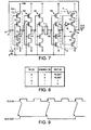
- Figure 8 illustrates a divide-by-four circuit.
- the divide-by-four circuit comprises four stages S1,S2,S3 and S4, and a tri-state inverter stage T connected in a ring with an input node of each stage connected to an output node of a preceding stage.
- Each of the four stages S1 to S4 has the transistor configuration described above with reference to Figure 1 in the divide-by-three circuit.
- the tri-state inverter stage T has an input node 2 connected to the output node of the preceding stage S4, an output node 4 which is connected to the input node of the transistor stage S1 and an enable input 6 which is connected to the clock nodes of the transistor stages S1 to S4.
- Tri-state inverters are known in the art and have the truth table shown in Figure 8, where the state marked "float" has the same meaning as that applied to the transistor stages S1 to S4.
- One exemplary circuit configuration of a tri-state inverter is illustrated in stage T of Figure 1, but it will be appreciated that other tri-state inverters can be used with the present invention.
- the tri-state inverter has a pair of p-channel transistors 10,12 connected between the supply voltage Vdd and the output node 4, and a pair of n-channel transistors 14,16 connected in series between the output node 4 and ground.
- the gates of the outermost transistors 10,16 are connected together to provide the input node 2 for the tri-state inverter.
- the gate of the innermost p-channel transistor 12 is connected to the enable input 6 via an inverter 18.
- the gate of the innermost n-channel transistor 14 is connected directly to the enable input 6.
- the enable input 6 receives the clock signal CLK IN supplied to the divide-by-four circuit, and thus acts as the clock node for the stage.
- the circuit of Figure 7 represents a divide-by-four counter, that is, one cycle of the output signal CLK OUT represents four cycles of the input signal CLK IN.
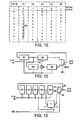
- the circuit causes a change in state in the output signal only on every other rising edge of the input signal. That this is the case can be seen by following through the effect of the truth tables of Figures 2 and 8, as in the following description of Figure 10.
- the logic state of the input signal CLK IN is high or logic one.
- the output signal CLK OUT has the same logic state as the input stage I1 for the first stage S1, and is marked V1 in Figure 10.
- V2 to V5 represent the output signals of the stages S1 to S4 respectively.
- V2 has logic value one
- V3 and V4 have logic value zero
- V5 has logic value one.
- the stage S1 has its clock node at zero and its input at zero, so that its output V2 remains at logic level one.
- the stage S2 still has an input signal V2 at logic state one, but because the state of the incoming signal CLK IN is now zero, the output node V3 now floats at logic state zero.
- the stage S3 now has an input state of zero, where the input signal CLK IN is zero, thus the state of its output changes to logic state one.
- the stage S4 now has a logic state of one at its input while the clock signal is low so that its output V5 floats at the preceding logic state one.
- the tri-state inverter stage T has an input signal at logic state one, while the state of the clock signal CLK IN is low, so that the output V1 floats at the preceding logic state, that is at logic state zero.
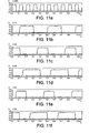
- Figure 11a represents an input waveform CLK IN having a duty cycle of 50%.
- Figure 11b shows the output signal at the output node 4 of the tri-state inverter stage (marked V1 in Figure 11b).
- the output signal is a divide-by-four version of the input clock signal and has a duty cycle of 50%.
- the outputs of the other transistor stages labelled V2 to V5 are shown in Figures 11c to 11f. These still represent a divide-by-four version of the input signals, but do not have a 50% duty cycle.
- FIG. 12 is a block diagram illustrating the concept underlying a programmable divider circuit.
- each block B1,B2,B3 and B4 represents a number of similar transistor stages of the type denoted S1 to S4 in the preceding description.
- Reference T denotes the tri-state inverter stage as described herein.
- the clock signal CLK IN is supplied to the clock nodes of the transistor stages in each sequence B1 to B4 and to the tri-state inverter stage T.
- a first sequence of transistor stages represented by blocks B1 and B2 are supplied to a first input of a multiplexer MUX.
- a second sequence of transistor stages comprising blocks B1,B3,T and B4 are supplied to a second input of the multiplexer MUX.
- the block B1 represents an input sequence of transistor stages, the first stage in the sequence of block B1 receiving the output signal from the multiplexer MUX.
- the output of the divider circuit CLK OUT is taken from the output of the multiplexer MUX.
- the multiplexer MUX has a select input which receives the select signal SEL which selects whether the block sequence B1,B2 or the block sequence B1,B3,T,B4 is connected in a ring.
- the number of stages in the blocks is selected so that the combination of blocks B1 and B2 provides an odd number N of transistor stages and the combination of blocks numbered B1,B3 and B4 provides an even number M of transistor stages.
- the divider ring can either contain N stages or M stages and the tri-state inverter stage T.
- the circuit acts as a divide-by-N counter and in the second case it acts as a divide-by-M counter.
- block B2 it is quite possible for block B2 to contain no transistor stages, so that the output of block B1 is connected directly to the first input of the multiplexer MUX.
- the output of the tri-state inverter T can be connected directly to the second input of the multiplexer MUX, in which case the block B4 has no transistor stages in it. This is required where the divider circuit is to generate an output signal CLK OUT having a 50% duty cycle.
- a single two-input multiplexer is illustrated in Figure 12, it will be appreciated from the following descriptions that a multiplexer having more than two inputs is possible, as is the provision of more than one multiplexer in the sequence of transistor stages. Thus, a variety of different possibilities are made available. A selection of particular examples is now described, but it will readily be appreciated that the principles underlying the present invention can be extended to provide a large number of different options for generating a programmable divider circuit.
- Figure 13 is a programmable divide-by-four/divide-by-five counter.
- the circuit has five transistor stages S1 to S5 connected in sequence.
- the circuit of Figure 13 also comprises a tri-state inverter stage T which has its input node 2 connected to the output of the fourth transistor stage S4.
- the enable node 6 of the tri-state inverter stage T receives the input signal CLK IN in the same manner as described above with reference to the divide-by-four circuit of Figure 7.
- a multiplexer 20 has a first input 22 connected to the output of the transistor stage S5 and a second output 24 connected to the output 4 of the tristate inverter stage T.
- the output of the multiplexer is connected to the input of the first transistor stage in the sequence S1.
- a select input 26 receives the select signal SEL which determines whether the first or second input of the multiplexer is connected to the output of the multiplexer.
- the circuit operates as a divide-by-five circuit.
- the output of the tri-state inverter stage T is connected to the input of the transistor stage S1
- the circuit operates as a divide-by-four circuit based on the principles discussed above with reference to Figure 7.
- the select signal SEL the circuit can selectively divide by four or five.
- Figure 14 illustrates operation of the circuit of Figure 13 with an input signal CLK IN having a 50% duty cycle as illustrated in Figure 14a.
- Figure 14b illustrates the state of the select signal SEL supplied to the select input of the multiplexer 20.
- the select signal SEL is low, causing the second input of the multiplexer to be supplied to its output, and thus connecting in a ring four of the transistor stages S1 to S4 and the tri-state inverter stage T.
- the circuit thus operates as a divide-by-four circuit, as can be seen from the output waveforms between time t0 and t1 in Figures 14c to 14i.
- the select signal SEL goes high, thus causing the first input 22 of the multiplexer 20 to be connected to its output. In this case therefore the five transistor stages S1 to S5 are connected in a ring so that the circuit operates as a divide-by-five circuit, as can be seen from the waveforms in Figures 14 c to 14i after time t1.
- the number of stages in the block B1 is not zero and thus the tri-state inverter stage T represents a branch which is selectively connectable in the divider ring.
- the circuit of Figure 15 which is a divide-by-three/divide-by-four programmable circuit.
- that circuit has the same configuration as the circuit of Figure 7, apart from the fact that a multiplexer MUX is now included to selectively connect the output of the third stage S3 or the output of the tri-state inverter stage T to the first stage S1 of the ring.
- the circuit either operates as a divide-by-three circuit or divide-by-four circuit.
- Figure 16 shows an example of a circuit which can selectively act as a divide-by-three, divide-by-four or divide-by-five counter.
- the circuit of Figure 16 has a structure very similar to that of Figure 13. That is, there are five similar transistor stages S1 to S5 connected in sequence and a tri-state inverter stage T connected as a branch in parallel with the fifth transistor stage S5. However, in place of the two input multiplexer 20, a three input multiplexer 30 is provided controllable by two select signals SELa and SELb. The first input 32 of the multiplexer is connected to the output of the fifth transistor stage S5. The second input 34 of the multiplexer 30 is connected to the output of the third transistor stage S3.
- the third input 36 of the multiplexer 30 is connected to the output of the tri-state inverter stage T.
- the truth table for the circuit of Figure 16 is shown in Figure 16a. That is, when the select signals SELa and SELb cause the first input 32 of the multiplexer 30 to be supplied to its output, the circuit acts as a divide-by-five counter. When the state of the select signals SELa and SELb cause the second input to be connected to the output of the multiplexer, the circuit acts as a divide-by-three counter. When the select signals SELa and SELb have states causing the third input of the multiplexer 30 to be connected to its output, the circuit acts as a divide-by-four circuit.
- the circuit of Figure 17 can be programmable to divide by one of four integers 2,3,4 or 5. Like Figure 13, the circuit comprises five similar transistor stages S1 to S5 connected in sequence, and a tri-state inverter stage T connected as a branch in parallel with the fifth transistor stage S5. However, in addition to the multiplexer 20, a second multiplexer 40 is connected in the circuit. The multiplexer 40 has one input 42 connected to the output of the third transistor stage and another input 43 connected to the output of the first transistor stage. The output of the multiplexer 40 feeds the fourth transistor stage S4. The second multiplexer 20 has one input 22 connected to the output of the fifth transistor stage S5 and another input 24 connected to the output of the tri-state inverter T.
- the output of the second multiplexer is supplied to the first transistor stage S1.
- the first multiplexer 40 is controlled by a select signal SEL1 and the second multiplexer 50 is controlled by a select signal SEL2.
- the truth table is shown in Figure 17a. That is, when the second input of the first multiplexer, and the second input of the second multiplexer are connected, then the circuit operates as a divide-by-two counter. When the first input of the first multiplexer and the second input of the second multiplexer are connected, the circuit operates as a divide-by-four counter. When the first input of the first multiplexer and the first input of the second multiplexer are connected, the counter operates as a divide-by-five counter.
- the counter When the second input of the first multiplexer and the first input of the second multiplexer are connected, the counter operates as a divide-by-three counter.
- FIG 18 is a diagram of a basic phase locked loop circuit in which the dividing circuits described herein are particularly useful.
- the phase locked loop receives a reference clock input REF CLK IN and generates a PLL clock output PLL CLK OUT.
- An input divider 50 creates from the reference clock input REF CLK IN a reference input frequency for a phase detector 52.
- the phase detector 52 also receives as an input a feedback signal ⁇ generated in a manner described in the following. If the two inputs to the phase detector differ in phase, an error output e is generated and is supplied to a charge pump 54.
- a loop filter 56 shapes the output of the charge pump 54 and generates a correction signal for a voltage controlled oscillator 58.
- the output of the voltage controlled oscillator is passed through a feedback divider 60 to generate the second input ⁇ to the phase detector.
- the output of the voltage controlled oscillator is also passed through an output divider 62 to generate the clock output PLL CLK OUT.
- a dividing circuit in accordance with the present invention can usefully be used to implement any of the input divider 50, feedback divider 60 or output divider 62 to provide a phase locked loop satisfying required technology, frequency and power constraints, in which the dividing factors are readily programmable.
Landscapes
- Manipulation Of Pulses (AREA)
- Pulse Circuits (AREA)
Applications Claiming Priority (2)
| Application Number | Priority Date | Filing Date | Title |
|---|---|---|---|
| GBGB9727245.4A GB9727245D0 (en) | 1997-12-23 | 1997-12-23 | A programmable divider circuit |
| GB9727245 | 1997-12-23 |
Publications (2)
| Publication Number | Publication Date |
|---|---|
| EP0926834A1 true EP0926834A1 (fr) | 1999-06-30 |
| EP0926834B1 EP0926834B1 (fr) | 2002-03-20 |
Family
ID=10824168
Family Applications (1)
| Application Number | Title | Priority Date | Filing Date |
|---|---|---|---|
| EP98310160A Expired - Lifetime EP0926834B1 (fr) | 1997-12-23 | 1998-12-11 | Circuit diviseur programmable |
Country Status (4)
| Country | Link |
|---|---|
| US (1) | US6133796A (fr) |
| EP (1) | EP0926834B1 (fr) |
| DE (1) | DE69804287T2 (fr) |
| GB (1) | GB9727245D0 (fr) |
Cited By (1)
| Publication number | Priority date | Publication date | Assignee | Title |
|---|---|---|---|---|
| WO2002029973A3 (fr) * | 2000-10-04 | 2002-08-01 | Broadcom Corp | Diviseur programmable a chaine de retard programmable integree pour des applications de puissance a faible vitesse et a vitesse elevee |
Families Citing this family (6)
| Publication number | Priority date | Publication date | Assignee | Title |
|---|---|---|---|---|
| US6278307B1 (en) * | 2000-07-24 | 2001-08-21 | Agere Systems Guardian Corp. | Method and apparatus for 50% duty-cycle programmable divided-down clock with even and odd divisor rates |
| US6445228B1 (en) | 2001-08-28 | 2002-09-03 | Xilinx, Inc. | Programmable even-number clock divider circuit with duty cycle correction and optional phase shift |
| US6714057B2 (en) | 2001-08-28 | 2004-03-30 | Xilinx, Inc. | Multi-purpose digital frequency synthesizer circuit for a programmable logic device |
| US6566918B1 (en) | 2001-08-28 | 2003-05-20 | Xilinx, Inc. | Divide-by-N clock divider circuit with minimal additional delay |
| KR100518226B1 (ko) * | 2003-04-23 | 2005-10-04 | 주식회사 하이닉스반도체 | Ddl 장치의 클락 분주기 및 그 클락 분주 방법 |
| US8442472B2 (en) * | 2011-04-04 | 2013-05-14 | Fujitsu Semiconductor Limited | Technique to generate divide by two and 25% duty cycle |
Citations (4)
| Publication number | Priority date | Publication date | Assignee | Title |
|---|---|---|---|---|
| US4389728A (en) * | 1979-12-29 | 1983-06-21 | Citizen Watch Co., Ltd. | Frequency divider |
| JPS6226920A (ja) * | 1985-07-29 | 1987-02-04 | Canon Inc | タイミング発生装置 |
| WO1990005413A1 (fr) * | 1988-10-31 | 1990-05-17 | Hughes Aircraft Company | Diviseur de frequence programmable numerique a haute vitesse |
| US4953187A (en) * | 1989-01-23 | 1990-08-28 | Motorola, Inc. | High speed prescaler |
Family Cites Families (5)
| Publication number | Priority date | Publication date | Assignee | Title |
|---|---|---|---|---|
| GB1373626A (en) * | 1970-11-27 | 1974-11-13 | Smiths Industries Ltd | Electrical dividing circuits |
| US4114049A (en) * | 1972-02-25 | 1978-09-12 | Tokyo Shibaura Electric Co., Ltd. | Counter provided with complementary field effect transistor inverters |
| JPS50147883A (fr) * | 1974-05-20 | 1975-11-27 | ||
| US5425074A (en) * | 1993-12-17 | 1995-06-13 | Intel Corporation | Fast programmable/resettable CMOS Johnson counters |
| FR2734966B1 (fr) * | 1995-05-31 | 1997-08-14 | Sgs Thomson Microelectronics | Diviseur programmable rapide |
-
1997
- 1997-12-23 GB GBGB9727245.4A patent/GB9727245D0/en not_active Ceased
-
1998
- 1998-12-11 DE DE69804287T patent/DE69804287T2/de not_active Expired - Fee Related
- 1998-12-11 EP EP98310160A patent/EP0926834B1/fr not_active Expired - Lifetime
- 1998-12-23 US US09/221,296 patent/US6133796A/en not_active Expired - Lifetime
Patent Citations (4)
| Publication number | Priority date | Publication date | Assignee | Title |
|---|---|---|---|---|
| US4389728A (en) * | 1979-12-29 | 1983-06-21 | Citizen Watch Co., Ltd. | Frequency divider |
| JPS6226920A (ja) * | 1985-07-29 | 1987-02-04 | Canon Inc | タイミング発生装置 |
| WO1990005413A1 (fr) * | 1988-10-31 | 1990-05-17 | Hughes Aircraft Company | Diviseur de frequence programmable numerique a haute vitesse |
| US4953187A (en) * | 1989-01-23 | 1990-08-28 | Motorola, Inc. | High speed prescaler |
Non-Patent Citations (1)
| Title |
|---|
| PATENT ABSTRACTS OF JAPAN vol. 011, no. 204 (E - 520) 2 July 1987 (1987-07-02) * |
Cited By (5)
| Publication number | Priority date | Publication date | Assignee | Title |
|---|---|---|---|---|
| WO2002029973A3 (fr) * | 2000-10-04 | 2002-08-01 | Broadcom Corp | Diviseur programmable a chaine de retard programmable integree pour des applications de puissance a faible vitesse et a vitesse elevee |
| US6518805B2 (en) | 2000-10-04 | 2003-02-11 | Broadcom Corporation | Programmable divider with built-in programmable delay chain for high-speed/low power application |
| US6661261B2 (en) | 2000-10-04 | 2003-12-09 | Broadcom Corporation | Programmable divider with built-in programmable delay chain for high-speed/low power application |
| US6882189B2 (en) | 2000-10-04 | 2005-04-19 | Broadcom Corporation | Programmable divider with built-in programmable delay chain for high-speed/low power application |
| US7005898B2 (en) | 2000-10-04 | 2006-02-28 | Broadcom Corporation | Programmable divider with built-in programmable delay chain for high-speed/low power application |
Also Published As
| Publication number | Publication date |
|---|---|
| DE69804287T2 (de) | 2002-11-21 |
| EP0926834B1 (fr) | 2002-03-20 |
| GB9727245D0 (en) | 1998-02-25 |
| DE69804287D1 (de) | 2002-04-25 |
| US6133796A (en) | 2000-10-17 |
Similar Documents
| Publication | Publication Date | Title |
|---|---|---|
| US6566918B1 (en) | Divide-by-N clock divider circuit with minimal additional delay | |
| US6744289B2 (en) | Clock divider circuit with duty cycle correction and minimal additional delay | |
| US4953187A (en) | High speed prescaler | |
| JP3758285B2 (ja) | 遅延回路およびそれを用いた発振回路 | |
| US7505548B2 (en) | Circuits and methods for programmable integer clock division with 50% duty cycle | |
| KR970006394B1 (ko) | 다상 클럭 발생 회로 | |
| US20050212570A1 (en) | Programmable frequency divider | |
| US20180054203A1 (en) | Wide Range Glitchless Switchable Clock Divider With Modified 2/3 Divider Stages | |
| JP3601961B2 (ja) | デュアル・モジュラス・プリスケーラ | |
| EP0483217B1 (fr) | Predemultiplicateur a vitesse elevee | |
| KR20010107751A (ko) | 타이밍차 분할 회로와 신호 제어 방법 및 장치 | |
| US5221863A (en) | Phase-locked loop clock signal generator | |
| WO1981002080A1 (fr) | Reseau de circuit dynamique sans rapport pour application a logique randomisee | |
| US6961403B1 (en) | Programmable frequency divider with symmetrical output | |
| US6501816B1 (en) | Fully programmable multimodulus prescaler | |
| EP0926834B1 (fr) | Circuit diviseur programmable | |
| US6967512B2 (en) | Multiphase-clock processing circuit and clock multiplying circuit | |
| JP7712054B2 (ja) | 高速マルチ係数cmosクロック分周器 | |
| US4715052A (en) | Frequency divide by N circuit | |
| EP0926833A1 (fr) | Circuit diviseur et étage à transistor pour celui-ci | |
| KR100967103B1 (ko) | 클럭생성회로 및 클럭생성방법 | |
| US7332945B2 (en) | Divider having dual modulus pre-scaler and an associated method | |
| US8466720B2 (en) | Frequency division of an input clock signal | |
| EP0926832B1 (fr) | Circuit diviseur pour diviser par des nombres pairs | |
| US6445760B1 (en) | Partially-synchronous high-speed counter circuits |
Legal Events
| Date | Code | Title | Description |
|---|---|---|---|
| PUAI | Public reference made under article 153(3) epc to a published international application that has entered the european phase |
Free format text: ORIGINAL CODE: 0009012 |
|
| AK | Designated contracting states |
Kind code of ref document: A1 Designated state(s): DE FR GB IT |
|
| AX | Request for extension of the european patent |
Free format text: AL;LT;LV;MK;RO;SI |
|
| 17P | Request for examination filed |
Effective date: 19991202 |
|
| AKX | Designation fees paid |
Free format text: DE FR GB IT |
|
| GRAG | Despatch of communication of intention to grant |
Free format text: ORIGINAL CODE: EPIDOS AGRA |
|
| 17Q | First examination report despatched |
Effective date: 20010126 |
|
| GRAG | Despatch of communication of intention to grant |
Free format text: ORIGINAL CODE: EPIDOS AGRA |
|
| GRAH | Despatch of communication of intention to grant a patent |
Free format text: ORIGINAL CODE: EPIDOS IGRA |
|
| GRAH | Despatch of communication of intention to grant a patent |
Free format text: ORIGINAL CODE: EPIDOS IGRA |
|
| REG | Reference to a national code |
Ref country code: GB Ref legal event code: IF02 |
|
| GRAA | (expected) grant |
Free format text: ORIGINAL CODE: 0009210 |
|
| AK | Designated contracting states |
Kind code of ref document: B1 Designated state(s): DE FR GB IT |
|
| PG25 | Lapsed in a contracting state [announced via postgrant information from national office to epo] |
Ref country code: IT Free format text: LAPSE BECAUSE OF FAILURE TO SUBMIT A TRANSLATION OF THE DESCRIPTION OR TO PAY THE FEE WITHIN THE PRESCRIBED TIME-LIMIT;WARNING: LAPSES OF ITALIAN PATENTS WITH EFFECTIVE DATE BEFORE 2007 MAY HAVE OCCURRED AT ANY TIME BEFORE 2007. THE CORRECT EFFECTIVE DATE MAY BE DIFFERENT FROM THE ONE RECORDED. Effective date: 20020320 |
|
| REF | Corresponds to: |
Ref document number: 69804287 Country of ref document: DE Date of ref document: 20020425 |
|
| ET | Fr: translation filed | ||
| ET | Fr: translation filed | ||
| PLBE | No opposition filed within time limit |
Free format text: ORIGINAL CODE: 0009261 |
|
| STAA | Information on the status of an ep patent application or granted ep patent |
Free format text: STATUS: NO OPPOSITION FILED WITHIN TIME LIMIT |
|
| 26N | No opposition filed |
Effective date: 20021223 |
|
| PGFP | Annual fee paid to national office [announced via postgrant information from national office to epo] |
Ref country code: GB Payment date: 20051207 Year of fee payment: 8 |
|
| PGFP | Annual fee paid to national office [announced via postgrant information from national office to epo] |
Ref country code: FR Payment date: 20051208 Year of fee payment: 8 |
|
| PGFP | Annual fee paid to national office [announced via postgrant information from national office to epo] |
Ref country code: DE Payment date: 20051209 Year of fee payment: 8 |
|
| PG25 | Lapsed in a contracting state [announced via postgrant information from national office to epo] |
Ref country code: DE Free format text: LAPSE BECAUSE OF NON-PAYMENT OF DUE FEES Effective date: 20070703 |
|
| GBPC | Gb: european patent ceased through non-payment of renewal fee |
Effective date: 20061211 |
|
| REG | Reference to a national code |
Ref country code: FR Ref legal event code: ST Effective date: 20070831 |
|
| PG25 | Lapsed in a contracting state [announced via postgrant information from national office to epo] |
Ref country code: GB Free format text: LAPSE BECAUSE OF NON-PAYMENT OF DUE FEES Effective date: 20061211 |
|
| PG25 | Lapsed in a contracting state [announced via postgrant information from national office to epo] |
Ref country code: FR Free format text: LAPSE BECAUSE OF NON-PAYMENT OF DUE FEES Effective date: 20070102 |