EP0926931A1 - Tableau de connexions a trous d'interconnexion - Google Patents
Tableau de connexions a trous d'interconnexion Download PDFInfo
- Publication number
- EP0926931A1 EP0926931A1 EP98914051A EP98914051A EP0926931A1 EP 0926931 A1 EP0926931 A1 EP 0926931A1 EP 98914051 A EP98914051 A EP 98914051A EP 98914051 A EP98914051 A EP 98914051A EP 0926931 A1 EP0926931 A1 EP 0926931A1
- Authority
- EP
- European Patent Office
- Prior art keywords
- vias
- wiring board
- interval
- sheath
- sheath portion
- Prior art date
- Legal status (The legal status is an assumption and is not a legal conclusion. Google has not performed a legal analysis and makes no representation as to the accuracy of the status listed.)
- Granted
Links
Images


Classifications
-
- H—ELECTRICITY
- H05—ELECTRIC TECHNIQUES NOT OTHERWISE PROVIDED FOR
- H05K—PRINTED CIRCUITS; CASINGS OR CONSTRUCTIONAL DETAILS OF ELECTRIC APPARATUS; MANUFACTURE OF ASSEMBLAGES OF ELECTRICAL COMPONENTS
- H05K3/00—Apparatus or processes for manufacturing printed circuits
- H05K3/46—Manufacturing multilayer circuits
-
- H—ELECTRICITY
- H10—SEMICONDUCTOR DEVICES; ELECTRIC SOLID-STATE DEVICES NOT OTHERWISE PROVIDED FOR
- H10W—GENERIC PACKAGES, INTERCONNECTIONS, CONNECTORS OR OTHER CONSTRUCTIONAL DETAILS OF DEVICES COVERED BY CLASS H10
- H10W70/00—Package substrates; Interposers; Redistribution layers [RDL]
- H10W70/60—Insulating or insulated package substrates; Interposers; Redistribution layers
- H10W70/62—Insulating or insulated package substrates; Interposers; Redistribution layers characterised by their interconnections
- H10W70/63—Vias, e.g. via plugs
- H10W70/635—Through-vias
-
- H—ELECTRICITY
- H05—ELECTRIC TECHNIQUES NOT OTHERWISE PROVIDED FOR
- H05K—PRINTED CIRCUITS; CASINGS OR CONSTRUCTIONAL DETAILS OF ELECTRIC APPARATUS; MANUFACTURE OF ASSEMBLAGES OF ELECTRICAL COMPONENTS
- H05K1/00—Printed circuits
- H05K1/02—Details
- H05K1/11—Printed elements for providing electric connections to or between printed circuits
- H05K1/115—Via connections; Lands around holes or via connections
-
- H—ELECTRICITY
- H05—ELECTRIC TECHNIQUES NOT OTHERWISE PROVIDED FOR
- H05K—PRINTED CIRCUITS; CASINGS OR CONSTRUCTIONAL DETAILS OF ELECTRIC APPARATUS; MANUFACTURE OF ASSEMBLAGES OF ELECTRICAL COMPONENTS
- H05K3/00—Apparatus or processes for manufacturing printed circuits
- H05K3/40—Forming printed elements for providing electric connections to or between printed circuits
- H05K3/4038—Through-connections; Vertical interconnect access [VIA] connections
-
- H—ELECTRICITY
- H05—ELECTRIC TECHNIQUES NOT OTHERWISE PROVIDED FOR
- H05K—PRINTED CIRCUITS; CASINGS OR CONSTRUCTIONAL DETAILS OF ELECTRIC APPARATUS; MANUFACTURE OF ASSEMBLAGES OF ELECTRICAL COMPONENTS
- H05K1/00—Printed circuits
- H05K1/02—Details
- H05K1/11—Printed elements for providing electric connections to or between printed circuits
- H05K1/111—Pads for surface mounting, e.g. lay-out
- H05K1/112—Pads for surface mounting, e.g. lay-out directly combined with via connections
-
- H—ELECTRICITY
- H05—ELECTRIC TECHNIQUES NOT OTHERWISE PROVIDED FOR
- H05K—PRINTED CIRCUITS; CASINGS OR CONSTRUCTIONAL DETAILS OF ELECTRIC APPARATUS; MANUFACTURE OF ASSEMBLAGES OF ELECTRICAL COMPONENTS
- H05K2201/00—Indexing scheme relating to printed circuits covered by H05K1/00
- H05K2201/09—Shape and layout
- H05K2201/09818—Shape or layout details not covered by a single group of H05K2201/09009 - H05K2201/09809
- H05K2201/09836—Oblique hole, via or bump
-
- H—ELECTRICITY
- H05—ELECTRIC TECHNIQUES NOT OTHERWISE PROVIDED FOR
- H05K—PRINTED CIRCUITS; CASINGS OR CONSTRUCTIONAL DETAILS OF ELECTRIC APPARATUS; MANUFACTURE OF ASSEMBLAGES OF ELECTRICAL COMPONENTS
- H05K2201/00—Indexing scheme relating to printed circuits covered by H05K1/00
- H05K2201/10—Details of components or other objects attached to or integrated in a printed circuit board
- H05K2201/10227—Other objects, e.g. metallic pieces
- H05K2201/10287—Metal wires as connectors or conductors
-
- H—ELECTRICITY
- H05—ELECTRIC TECHNIQUES NOT OTHERWISE PROVIDED FOR
- H05K—PRINTED CIRCUITS; CASINGS OR CONSTRUCTIONAL DETAILS OF ELECTRIC APPARATUS; MANUFACTURE OF ASSEMBLAGES OF ELECTRICAL COMPONENTS
- H05K2201/00—Indexing scheme relating to printed circuits covered by H05K1/00
- H05K2201/10—Details of components or other objects attached to or integrated in a printed circuit board
- H05K2201/10613—Details of electrical connections of non-printed components, e.g. special leads
- H05K2201/10954—Other details of electrical connections
- H05K2201/10977—Encapsulated connections
-
- H—ELECTRICITY
- H05—ELECTRIC TECHNIQUES NOT OTHERWISE PROVIDED FOR
- H05K—PRINTED CIRCUITS; CASINGS OR CONSTRUCTIONAL DETAILS OF ELECTRIC APPARATUS; MANUFACTURE OF ASSEMBLAGES OF ELECTRICAL COMPONENTS
- H05K2203/00—Indexing scheme relating to apparatus or processes for manufacturing printed circuits covered by H05K3/00
- H05K2203/02—Details related to mechanical or acoustic processing, e.g. drilling, punching, cutting, using ultrasound
- H05K2203/0235—Laminating followed by cutting or slicing perpendicular to plane of the laminate; Embedding wires in an object and cutting or slicing the object perpendicular to direction of the wires
-
- H—ELECTRICITY
- H10—SEMICONDUCTOR DEVICES; ELECTRIC SOLID-STATE DEVICES NOT OTHERWISE PROVIDED FOR
- H10W—GENERIC PACKAGES, INTERCONNECTIONS, CONNECTORS OR OTHER CONSTRUCTIONAL DETAILS OF DEVICES COVERED BY CLASS H10
- H10W44/00—Electrical arrangements for controlling or matching impedance
- H10W44/20—Electrical arrangements for controlling or matching impedance at high-frequency [HF] or radio frequency [RF]
- H10W44/203—Electrical connections
- H10W44/209—Vertical interconnections, e.g. vias
- H10W44/212—Coaxial feed-throughs in substrates
-
- H—ELECTRICITY
- H10—SEMICONDUCTOR DEVICES; ELECTRIC SOLID-STATE DEVICES NOT OTHERWISE PROVIDED FOR
- H10W—GENERIC PACKAGES, INTERCONNECTIONS, CONNECTORS OR OTHER CONSTRUCTIONAL DETAILS OF DEVICES COVERED BY CLASS H10
- H10W70/00—Package substrates; Interposers; Redistribution layers [RDL]
- H10W70/60—Insulating or insulated package substrates; Interposers; Redistribution layers
- H10W70/62—Insulating or insulated package substrates; Interposers; Redistribution layers characterised by their interconnections
- H10W70/65—Shapes or dispositions of interconnections
- H10W70/654—Top-view layouts
- H10W70/655—Fan-out layouts
Definitions
- the present invention relates to a wiring board. More particularly, the present invention relates to a wiring board having a plurality of vias penetrating the wiring board from one side to the other side, which are radially extending from one side to the other side of the wiring board so that the interval between the vias on one side can be smaller than that between the vias on the other side.
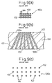
- this wiring board is composed as follows. Vias 102, 102, ⁇ ⁇ , which penetrate a wiring board 100 made of resin from one side 100a to the other side 100b, are radially extending along the direction from one side 100a to the other side 100b. As can be seen in Fig. 9(a) showing a state on one side 100a of the wiring board 100 and can also be seen in Fig. 9(c) showing a state on the other side 100b, interval Wa between the vias on one side 100a of the wiring board 100 is smaller than interval Wc between the vias on the other side 100b.
- the vias 102, 102, ⁇ ⁇ are arranged on one side 100a of the wiring board 100 at high density so that flip chip type semiconductor elements (not shown), on the bottom surfaces of which a large number of bumps to be used as electrode terminals are provided, can be mounted on one side 100a, the vias 102, 102, ⁇ ⁇ can be arranged on the other side 100b of the wiring board 100 at low density so that external connecting terminals can be mounted. Due to the above arrangement, it is possible to provide a wiring board on which flip chip type semiconductor elements, which have been highly accumulated, can be mounted.
- the inventors of the present application made investigation to solve the above problems. As a result of the investigation, the following knowledge has been found.
- an electric conductor forming the via is covered with an organic insulator, even if the interval between the vias provided on one side of the wiring board is extremely reduced, there is no possibility that the electric conductors are contacted and short-circuited to each other. In this way, the inventors have accomplished the invention.
- the present invention provides a wiring board characterized in that: a plurality of vias penetrating from one side to the other side of the wiring board are radially formed in the direction from one side to the other side of the wiring board so that an interval between the vias on one side of the wiring board can be made smaller than an interval between the vias on the other side; and the vias are coated with sheath portions made of the same electric conductor as that forming the cores of the vias.
- the interval between the vias of which is smaller than that on the other side, when the vias are formed so that at least some of the sheath portions of the vias are in contact with the sheath portions of the adjacent vias, it is possible to form the vias on one side of the wiring board at high density.
- the present invention provides a wiring board characterized in that: a plurality of vias penetrating from one side to the other side of the wiring board are radially formed in the direction from one side to the other side of the wiring board so that the interval between the vias on one side of the wiring board can be made smaller than the interval between the vias on the other side; an electric conductor forming a core of the via is coated with a first sheath portion made of an insulator; and the first sheath portion is coated with a second sheath portion which is a conductor layer.
- the interval between the vias of which is smaller than that on the other side, when the vias are formed so that at least some of the second sheath portions of the vias can be contacted with the second sheath portions of the adjacent vias, it is possible to form the vias on one side of the wiring board at high density.
- the second sheath portion made of a conductor is electrically connected to a ground line formed on the wiring board, it is possible to form a coaxial-cable-like via in which the core made of a conductor is surrounded and shielded by the second sheath portion.
- the thus formed wiring board can be applied to a device in which high frequency is used.
- the outer circumferential surface of the metallic wire of the via is coated with an insulator and the outer circumferential surface of the insulator is coated with a conductor layer, it is possible to form a via of the two layer structure.
- the conductor forming the core of the via is coated with the sheath portion made of an insulator. Therefore, even when the sheath portion of the via is contacted with the sheath portion of the adjacent via, there is no possibility that the cores are contacted and short-circuited with each other.
- the interval between vias on one side of the wiring board can be further reduced. Accordingly, the density of the wiring board can be further increased in accordance with the demand for high integration of semiconductors.
- Figs. 1(a) to 1(c) are cross-sectional views showing a wiring board having vias according to an embodiment of the present invention.
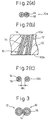
- Figs. 2(a) to 2(c) are schematic illustrations showing a portion of the wiring board.
- the wiring board of the present invention is composed in such a manner that vias 12, 12, ⁇ ⁇ penetrating the wiring board 10 made of resin from one side 10a (the upper side in the drawing) to the other side 10b (the lower side in the drawing) radially extend along the direction from one side 10a to the other side 10b.
- Fig. 1(a) showing a state of one side 10a of the wiring board 10 and can also be seen in Fig.
- interval Wa between the vias on one side 10a of the wiring board 10 is smaller than the interval Wb between the vias on the other side 10b.
- interval Wa is substantially zero.
- This via 12 includes a core and sheath structure (two layer structure) in which the core portion 14 made of an electric conductor such as copper or aluminum is coated with a sheath portion 16 made of an insulator. Since the interval Wa is zero on one side 10a, the via 12 substantially comes into contact with the adjacent via 12 through the sheath portion 16 on one side 10a of the wiring board 10.
- the interval Wa between the vias is extremely small on one side 10a, and even when the sheath portions 16 of the vias 12, 12 are in contact with each other as shown in Fig. 3, or even when the sheath portions 16 of the vias 12, 12 are pushed to each other, it is possible to prevent the core portions 14 from being short-circuited to each other because the core portions 14 made of a conductor are electrically insulated from each other by the sheath portions 16.
- the vias 12 constituting the wiring board may be made of wires of metal such as copper or aluminum which are coated with an insulating material.
- Examples of usable insulating materials to insulate the vias 12 are organic insulating materials such as polyimide, epoxy, maleimide, cyanate ester, polyphenyl ether, polyolefine, silicon and aromatic resin. Insulating material to be used may be either of a thermosetting type or a thermoplastic type, however, it is preferable to use flexible material.
- inorganic filler is mixed with insulating material because the coefficient of thermal expansion can be reduced, the radiating property can be enhanced and the mechanical strength can be enhanced.
- examples of usable inorganic filler are inorganic powder or short fiber of alumina, silica glass, aluminum nitride and mullite.
- the thickness of the insulating material that is, the thickness of the sheath portion 16 is determined by a via pitch (distance between the centers of the adjacent vias) and the via diameter on one side 10a of the wiring board 10.
- a via pitch distance between the centers of the adjacent vias
- the via diameter on one side 10a of the wiring board 10 For example, in the case where the vias 12, 12, ⁇ ⁇ , the diameter of which is 100 ⁇ m, are arranged at the via pitch of 250 ⁇ m on one side 10a of the wiring board 10 while the sheath portions 16 of the adjoining vias 12 are in contact with each other, it is possible to use a metallic wire, the diameter of which is 100 ⁇ m, coated with an insulator, the thickness of which is 75 ⁇ m.
- the vias 12 shown in Figs. 1(a) to 2(c) are formed into straight lines, however, it is possible to use vias, a portion of which is formed into a curved line.
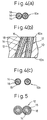
- the vias 12 On the wiring boards shown in Figs. 1(a) to 1(c) and Figs. 2(a) to 2(c), the vias 12 have a two layer structure in which the core portion 14 made of a conductor is coated with the sheath portion 16 made of an insulator. However, as shown in Figs. 4(a) to 4(c), the vias 12 may be composed of a three layer structure.
- the vias 12 of the second embodiment are composed of a three layer structure, the detail of which is described as follows.
- the core portion 14 made of a conductor such as copper or aluminum is coated with the first sheath portion 16 made of an insulator.
- the first sheath portion 16 is coated with the second sheath portion 18 made of a conductor layer.
- the sheath portion 18 of the via 12 in the second embodiment is connected to a ground line arranged on the wiring board 10, it is possible to form a coaxial-cable-like via 12 in which the conductor of the core portion 14 is surrounded and shielded by the sheath portion 18. Therefore, it is possible to provide a wiring board 10 to be used for signals of high frequency.
- the conductor to form the above second sheath portion 18 can be provided when a conductor layer made of metal such as copper is formed on the circumferential surface of the first sheath portion 16 by means of electroless plating.
- a plurality of wires 20, 20, ⁇ ⁇ in which metallic wires made of metal such as copper or aluminum are coated with the sheath portions made of insulating material, are arranged in parallel to each other while predetermined intervals are left as shown in Fig. 6.
- a plurality of wires 20, 20, ⁇ ⁇ in which metallic wires made of metal such as copper or aluminum are coated with the first sheath portions made of insulating material and the first sheath portion is coated with the second sheath portion made of a conductor, are arranged in parallel to each other while the predetermined intervals are left as shown in Fig. 6.
- the wires 20, 20, ⁇ ⁇ arranged in parallel to each other at predetermined intervals as shown in Fig. 6 are made up into a bundle as shown in Fig. 7.
- the wires 20, 20, ⁇ ⁇ can be easily bundled by inserting a bundling tool 24, 24 between the guide plates 22a, 22b in parallel.
- the lengths of some wires, which are pushed by the bundling tool 24, 24, are increased so that they longer than the distance between the guide plates 22a, 22b shown in Fig. 6. Therefore, it is preferable that diameters of the guide holes formed on the guide plates 22a, 22b are sufficiently large so that the wires 20 can be freely moved in the guide holes.
- a fluid precursor may be poured and solidified.
- the intervals of the vias 12 arranged on one side of the wiring board 10 can be extremely reduced, and it is possible to mount highly accumulated flip chip type semiconductor elements, on the bottom surfaces of which a large number of bumps to be used as electrode terminals are provided, on one side of the wiring boards 10.
- the wiring board of the present invention on one side of the wiring board, it is possible to further reduce the intervals of the vias. On the other side of the wiring board, it is possible to extend the intervals of the vias as much as required. Therefore, external connecting terminals can be easily attached onto the other side of the wiring board. Accordingly, the density of the wiring board of the present invention is sufficiently high so that highly accumulated semiconductor elements can be mounted on the wiring board.
Landscapes
- Engineering & Computer Science (AREA)
- Microelectronics & Electronic Packaging (AREA)
- Manufacturing & Machinery (AREA)
- Production Of Multi-Layered Print Wiring Board (AREA)
- Insulated Metal Substrates For Printed Circuits (AREA)
- Printing Elements For Providing Electric Connections Between Printed Circuits (AREA)
Applications Claiming Priority (3)
| Application Number | Priority Date | Filing Date | Title |
|---|---|---|---|
| JP09868197A JP3629348B2 (ja) | 1997-04-16 | 1997-04-16 | 配線基板 |
| JP9868197 | 1997-04-16 | ||
| PCT/JP1998/001746 WO1998047326A1 (fr) | 1997-04-16 | 1998-04-16 | Tableau de connexions a trous d'interconnexion |
Publications (3)
| Publication Number | Publication Date |
|---|---|
| EP0926931A1 true EP0926931A1 (fr) | 1999-06-30 |
| EP0926931A4 EP0926931A4 (fr) | 2006-12-06 |
| EP0926931B1 EP0926931B1 (fr) | 2008-01-16 |
Family
ID=14226262
Family Applications (1)
| Application Number | Title | Priority Date | Filing Date |
|---|---|---|---|
| EP98914051A Expired - Lifetime EP0926931B1 (fr) | 1997-04-16 | 1998-04-16 | Tableau de connexions a trous d'interconnexion |
Country Status (6)
| Country | Link |
|---|---|
| US (1) | US6271483B1 (fr) |
| EP (1) | EP0926931B1 (fr) |
| JP (1) | JP3629348B2 (fr) |
| KR (1) | KR100281381B1 (fr) |
| DE (1) | DE69839006T2 (fr) |
| WO (1) | WO1998047326A1 (fr) |
Cited By (3)
| Publication number | Priority date | Publication date | Assignee | Title |
|---|---|---|---|---|
| EP1492168A4 (fr) * | 2002-03-08 | 2007-03-28 | Hamamatsu Photonics Kk | Detecteur |
| US7230247B2 (en) | 2002-03-08 | 2007-06-12 | Hamamatsu Photonics K.K. | Detector |
| EP1775761A4 (fr) * | 2004-07-06 | 2007-08-29 | Tokyo Electron Ltd | Substrat traversant et dispositif d"interposition, et procede de fabrication de substrat traversant |
Families Citing this family (14)
| Publication number | Priority date | Publication date | Assignee | Title |
|---|---|---|---|---|
| TW434821B (en) * | 2000-02-03 | 2001-05-16 | United Microelectronics Corp | Allocation structure of via plug to connect different metal layers |
| US6774315B1 (en) * | 2000-05-24 | 2004-08-10 | International Business Machines Corporation | Floating interposer |
| US6815621B2 (en) * | 2000-10-02 | 2004-11-09 | Samsung Electronics Co., Ltd. | Chip scale package, printed circuit board, and method of designing a printed circuit board |
| KR20030065698A (ko) * | 2002-01-30 | 2003-08-09 | 삼성전자주식회사 | 볼의 피치가 작은 반도체 패키지의 테스트를 용이하게 할수 있는 반도체 패키지 테스트 보드 |
| KR20050065038A (ko) * | 2003-12-24 | 2005-06-29 | 삼성전기주식회사 | 비수직 비아가 구비된 인쇄회로기판 및 패키지 |
| US20050251777A1 (en) * | 2004-05-05 | 2005-11-10 | International Business Machines Corporation | Method and structure for implementing enhanced electronic packaging and PCB layout with diagonal vias |
| US7915537B1 (en) * | 2005-10-19 | 2011-03-29 | Edward Herbert | Interposer and method for making interposers |
| US7629541B2 (en) * | 2006-06-19 | 2009-12-08 | Endicott Interconnect Technologies, Inc. | High speed interposer |
| CN103891425B (zh) | 2011-10-21 | 2017-06-13 | 株式会社村田制作所 | 多层布线基板、探针卡以及多层布线基板的制造方法 |
| US8946757B2 (en) * | 2012-02-17 | 2015-02-03 | Invensas Corporation | Heat spreading substrate with embedded interconnects |
| JP2014038884A (ja) * | 2012-08-10 | 2014-02-27 | Murata Mfg Co Ltd | 電子部品および電子部品の製造方法 |
| US9496212B2 (en) * | 2014-12-19 | 2016-11-15 | Freescale Semiconductor, Inc. | Substrate core via structure |
| US20200072871A1 (en) * | 2017-03-31 | 2020-03-05 | Intel Corporation | Ultra low-cost, low leadtime, and high density space transformer for fine pitch applications |
| CN117546370A (zh) * | 2021-07-28 | 2024-02-09 | 弗劳恩霍夫应用研究促进协会 | 接触装置、接触装置制造方法及组件 |
Family Cites Families (14)
| Publication number | Priority date | Publication date | Assignee | Title |
|---|---|---|---|---|
| JPS56146264A (en) * | 1980-04-14 | 1981-11-13 | Mitsubishi Electric Corp | Carrier for equipment of chip |
| JPS63193587A (ja) * | 1987-02-06 | 1988-08-10 | 株式会社日立製作所 | 導体シ−ルド付微細スルホ−ル基板 |
| US5197892A (en) * | 1988-05-31 | 1993-03-30 | Canon Kabushiki Kaisha | Electric circuit device having an electric connecting member and electric circuit components |
| US5055966A (en) * | 1990-12-17 | 1991-10-08 | Hughes Aircraft Company | Via capacitors within multi-layer, 3 dimensional structures/substrates |
| JP3167141B2 (ja) * | 1991-04-16 | 2001-05-21 | 日本特殊陶業株式会社 | 集積回路用パッケージ |
| JP3004071B2 (ja) * | 1991-04-16 | 2000-01-31 | 日本特殊陶業株式会社 | 集積回路用パッケージ |
| US5315072A (en) * | 1992-01-27 | 1994-05-24 | Hitachi Seiko, Ltd. | Printed wiring board having blind holes |
| US5340947A (en) * | 1992-06-22 | 1994-08-23 | Cirqon Technologies Corporation | Ceramic substrates with highly conductive metal vias |
| JP2570617B2 (ja) * | 1994-05-13 | 1997-01-08 | 日本電気株式会社 | 多層配線セラミック基板のビア構造及びその製造方法 |
| JP3252635B2 (ja) * | 1995-01-13 | 2002-02-04 | 株式会社村田製作所 | 積層電子部品 |
| JPH08330469A (ja) * | 1995-05-30 | 1996-12-13 | Hitachi Ltd | 半導体装置用配線基板およびその製造方法 |
| US5699613A (en) * | 1995-09-25 | 1997-12-23 | International Business Machines Corporation | Fine dimension stacked vias for a multiple layer circuit board structure |
| US5920123A (en) * | 1997-01-24 | 1999-07-06 | Micron Technology, Inc. | Multichip module assembly having via contacts and method of making the same |
| US5949030A (en) * | 1997-11-14 | 1999-09-07 | International Business Machines Corporation | Vias and method for making the same in organic board and chip carriers |
-
1997
- 1997-04-16 JP JP09868197A patent/JP3629348B2/ja not_active Expired - Fee Related
-
1998
- 1998-04-16 US US09/202,432 patent/US6271483B1/en not_active Expired - Fee Related
- 1998-04-16 KR KR1019980710276A patent/KR100281381B1/ko not_active Expired - Fee Related
- 1998-04-16 WO PCT/JP1998/001746 patent/WO1998047326A1/fr not_active Ceased
- 1998-04-16 DE DE69839006T patent/DE69839006T2/de not_active Expired - Lifetime
- 1998-04-16 EP EP98914051A patent/EP0926931B1/fr not_active Expired - Lifetime
Cited By (4)
| Publication number | Priority date | Publication date | Assignee | Title |
|---|---|---|---|---|
| EP1492168A4 (fr) * | 2002-03-08 | 2007-03-28 | Hamamatsu Photonics Kk | Detecteur |
| US7230247B2 (en) | 2002-03-08 | 2007-06-12 | Hamamatsu Photonics K.K. | Detector |
| EP1775761A4 (fr) * | 2004-07-06 | 2007-08-29 | Tokyo Electron Ltd | Substrat traversant et dispositif d"interposition, et procede de fabrication de substrat traversant |
| US7866038B2 (en) | 2004-07-06 | 2011-01-11 | Tokyo Electron Limited | Through substrate, interposer and manufacturing method of through substrate |
Also Published As
| Publication number | Publication date |
|---|---|
| EP0926931A4 (fr) | 2006-12-06 |
| JP3629348B2 (ja) | 2005-03-16 |
| EP0926931B1 (fr) | 2008-01-16 |
| JPH10290059A (ja) | 1998-10-27 |
| DE69839006D1 (de) | 2008-03-06 |
| US6271483B1 (en) | 2001-08-07 |
| KR100281381B1 (ko) | 2001-02-01 |
| KR20000016676A (ko) | 2000-03-25 |
| WO1998047326A1 (fr) | 1998-10-22 |
| DE69839006T2 (de) | 2009-01-08 |
Similar Documents
| Publication | Publication Date | Title |
|---|---|---|
| US6271483B1 (en) | Wiring board having vias | |
| US7508079B2 (en) | Circuit substrate and method of manufacturing the same | |
| KR100295933B1 (ko) | 비아형성방법및이에의한비아구조체 | |
| JP3419348B2 (ja) | 集積回路素子接続用ケーブルおよびその製造方法 | |
| US7435913B2 (en) | Slanted vias for electrical circuits on circuit boards and other substrates | |
| US20010001292A1 (en) | Through-chip conductors for low inductance chip-to-chip integration and off-chip connections | |
| US6307261B1 (en) | Method for the manufacturing of a semiconductor device which comprises at least one chip and corresponding device | |
| US8723337B2 (en) | Structure for high-speed signal integrity in semiconductor package with single-metal-layer substrate | |
| US4956749A (en) | Interconnect structure for integrated circuits | |
| US6407343B1 (en) | Multilayer wiring board | |
| US20060118934A1 (en) | Multi-level semiconductor module and method for fabricating the same | |
| EP1344435B1 (fr) | Substrat plan parallele | |
| US7420131B2 (en) | Wiring substrate | |
| US9713258B2 (en) | Integrated circuit chip packaging | |
| GB2168857A (en) | Method and structure for interconnecting high frequency components | |
| US6238777B1 (en) | Printed-circuit board | |
| US4674808A (en) | Signal ground planes for tape bonded devices | |
| US20060145350A1 (en) | High frequency conductors for packages of integrated circuits | |
| US6302732B1 (en) | Coaxial connection apparatus and method of attachment | |
| US20020166696A1 (en) | Land grid array (LGA) pad repair structure and method | |
| US20020041009A1 (en) | Transmission line assembly chip and a manufacturing method thereof in a multi-chip module | |
| JP2001102517A (ja) | 回路装置 | |
| US20040182265A1 (en) | Wiring substrate | |
| US20190057796A1 (en) | Wire with composite shield | |
| KR100271793B1 (ko) | 다층인쇄회로기판의층간배선연결방법 |
Legal Events
| Date | Code | Title | Description |
|---|---|---|---|
| PUAI | Public reference made under article 153(3) epc to a published international application that has entered the european phase |
Free format text: ORIGINAL CODE: 0009012 |
|
| 17P | Request for examination filed |
Effective date: 19990113 |
|
| AK | Designated contracting states |
Kind code of ref document: A1 Designated state(s): DE FR GB |
|
| A4 | Supplementary search report drawn up and despatched |
Effective date: 20061027 |
|
| 17Q | First examination report despatched |
Effective date: 20070327 |
|
| GRAP | Despatch of communication of intention to grant a patent |
Free format text: ORIGINAL CODE: EPIDOSNIGR1 |
|
| RIC1 | Information provided on ipc code assigned before grant |
Ipc: H01L 23/498 20060101ALN20070705BHEP Ipc: H05K 1/11 20060101AFI20070705BHEP |
|
| GRAS | Grant fee paid |
Free format text: ORIGINAL CODE: EPIDOSNIGR3 |
|
| GRAA | (expected) grant |
Free format text: ORIGINAL CODE: 0009210 |
|
| AK | Designated contracting states |
Kind code of ref document: B1 Designated state(s): DE FR GB |
|
| REG | Reference to a national code |
Ref country code: GB Ref legal event code: FG4D |
|
| REF | Corresponds to: |
Ref document number: 69839006 Country of ref document: DE Date of ref document: 20080306 Kind code of ref document: P |
|
| ET | Fr: translation filed | ||
| PLBE | No opposition filed within time limit |
Free format text: ORIGINAL CODE: 0009261 |
|
| STAA | Information on the status of an ep patent application or granted ep patent |
Free format text: STATUS: NO OPPOSITION FILED WITHIN TIME LIMIT |
|
| 26N | No opposition filed |
Effective date: 20081017 |
|
| PGFP | Annual fee paid to national office [announced via postgrant information from national office to epo] |
Ref country code: GB Payment date: 20100325 Year of fee payment: 13 |
|
| PGFP | Annual fee paid to national office [announced via postgrant information from national office to epo] |
Ref country code: FR Payment date: 20100521 Year of fee payment: 13 |
|
| PGFP | Annual fee paid to national office [announced via postgrant information from national office to epo] |
Ref country code: DE Payment date: 20100430 Year of fee payment: 13 |
|
| REG | Reference to a national code |
Ref country code: DE Ref legal event code: R119 Ref document number: 69839006 Country of ref document: DE |
|
| REG | Reference to a national code |
Ref country code: DE Ref legal event code: R119 Ref document number: 69839006 Country of ref document: DE |
|
| GBPC | Gb: european patent ceased through non-payment of renewal fee |
Effective date: 20110416 |
|
| REG | Reference to a national code |
Ref country code: FR Ref legal event code: ST Effective date: 20111230 |
|
| PG25 | Lapsed in a contracting state [announced via postgrant information from national office to epo] |
Ref country code: FR Free format text: LAPSE BECAUSE OF NON-PAYMENT OF DUE FEES Effective date: 20110502 |
|
| PG25 | Lapsed in a contracting state [announced via postgrant information from national office to epo] |
Ref country code: GB Free format text: LAPSE BECAUSE OF NON-PAYMENT OF DUE FEES Effective date: 20110416 |
|
| PG25 | Lapsed in a contracting state [announced via postgrant information from national office to epo] |
Ref country code: DE Free format text: LAPSE BECAUSE OF NON-PAYMENT OF DUE FEES Effective date: 20111031 |