EP0928101A2 - Matrice de capteurs CMOS - Google Patents
Matrice de capteurs CMOS Download PDFInfo
- Publication number
- EP0928101A2 EP0928101A2 EP98310649A EP98310649A EP0928101A2 EP 0928101 A2 EP0928101 A2 EP 0928101A2 EP 98310649 A EP98310649 A EP 98310649A EP 98310649 A EP98310649 A EP 98310649A EP 0928101 A2 EP0928101 A2 EP 0928101A2
- Authority
- EP
- European Patent Office
- Prior art keywords
- transistor
- reset
- voltage
- supply voltage
- sensing
- Prior art date
- Legal status (The legal status is an assumption and is not a legal conclusion. Google has not performed a legal analysis and makes no representation as to the accuracy of the status listed.)
- Withdrawn
Links
Images
Classifications
-
- H—ELECTRICITY
- H04—ELECTRIC COMMUNICATION TECHNIQUE
- H04N—PICTORIAL COMMUNICATION, e.g. TELEVISION
- H04N25/00—Circuitry of solid-state image sensors [SSIS]; Control thereof
- H04N25/60—Noise processing, e.g. detecting, correcting, reducing or removing noise
- H04N25/65—Noise processing, e.g. detecting, correcting, reducing or removing noise applied to reset noise, e.g. KTC noise related to CMOS structures by techniques other than CDS
-
- H—ELECTRICITY
- H04—ELECTRIC COMMUNICATION TECHNIQUE
- H04N—PICTORIAL COMMUNICATION, e.g. TELEVISION
- H04N25/00—Circuitry of solid-state image sensors [SSIS]; Control thereof
- H04N25/60—Noise processing, e.g. detecting, correcting, reducing or removing noise
- H04N25/67—Noise processing, e.g. detecting, correcting, reducing or removing noise applied to fixed-pattern noise, e.g. non-uniformity of response
-
- H—ELECTRICITY
- H04—ELECTRIC COMMUNICATION TECHNIQUE
- H04N—PICTORIAL COMMUNICATION, e.g. TELEVISION
- H04N25/00—Circuitry of solid-state image sensors [SSIS]; Control thereof
- H04N25/70—SSIS architectures; Circuits associated therewith
- H04N25/76—Addressed sensors, e.g. MOS or CMOS sensors
- H04N25/77—Pixel circuitry, e.g. memories, A/D converters, pixel amplifiers, shared circuits or shared components
Definitions
- the invention relates to imaging sensors, more especially to CMOS imaging sensors.
- CCD imagers based on the charged couple device (“CCD") are in widespread use.
- CCD imager circuits require a manufacturing process which is incompatible with standard CMOS processing.
- CCD imager circuits cannot be integrated on a single chip with other circuits that provide support functions. For example, separate CCD control, A/D conversion, and signal processing chips are needed.
- the operation of a CCD imager also requires multiple voltage supplies varying from, e.g. 5V to 12V.
- CMOS imagers have also been previously proposed as imagers, but their use has been limited.
- FPN Fixed Pattem Noise
- Each pixel circuit comprises at least a photodiode and a sensing transistor (operating as source-follower) as shown in Figure 2 of the accompanying drawings.
- Mismatches of the sensing transistor between pixels may produce different output levels for a given input optical signal. The variations of these output levels is called pixel FPN.
- each column (or row) has separate read circuitry.
- Driver mismatches between different columns (or rows) produce column FPN.
- Most device mismatches are caused by threshold voltage (V T ) mismatches among CMOS transistors across the wafer.
- a conventional way of FPN suppression is to use a memory block to store the signal data for a whole frame and to subtract the FPN by sampling a reset voltage for the whole frame. The subtraction is done on a frame-by-frame basis and tends to result in slow frame rates.
- CDS Correlated Double Sampling
- a technique for suppressing fixed pattern noise derived from a pixel reset switch based on a mismatch Independent Reset Sensing (“MIRS”) technique which enables reset-switch sensing in SCDS or CDS architectures to be independent of NMOS switching device variations. This is achieved by ensuring that the reset switch operates in its linear region when turned ON. Therefore, even if mismatch effects exist in an NMOS reset switching device, the mismatch effect will not produce PFN on the pixel readout.
- MIRS mismatch Independent Reset Sensing
- the MIRS technique can be implemented so that the reset switch mismatch effects in a CMOS area array sensor will not produce FPN at the output.
- MIRS optionally together with the SCDS technique of the cross-referenced application, can suppress FPN by 1/25 to 1/20. Therefore, wide-spread application of CMOS imagers can be realized.
- Another advantage is that the technique can be easily integrated with other CDS techniques.
- Another advantage is that the method can provide a full-integrated and low-cost solution with a single chip incorporating all the necessary digital circuits for the CMOS imager system.
- a method for operating a pixel circuit in a photosensing integrated circuit comprising the steps of: turning on a reset transistor, using a reset gate voltage which is more in magnitude than any source/drain voltage of said reset transistor by a value of at least the sum of one threshold voltage plus the maximum threshold variation of the given process; and, after turning off said reset transistor, allowing a photosensing device to apply a illumination-dependent current to one of said source/drain terminals of a sensing transistor for a desired integration time; and thereafter sensing the voltage on said one source/drain terminal of said reset transistor.
- a method for operating a photosensing device comprising the steps of: providing a first supply voltage to a reset transistor, and turning on said reset transistor with a reset gate voltage which is approximately equal to a second supply voltage which exceeds in magnitude said first supply voltage; wherein said first supply voltage is always less in magnitude than said second supply voltage by at least the sum of one threshold voltage plus the maximum threshold variation of the given process; and wherein said reset transistor is connected to apply an initial voltage, which is precisely equal to said first supply voltage, regardless of the threshold voltage of said reset transistor, to the gate of a sensing transistor; and allowing a photosensing device to apply a illumination-dependent current to said gate of said sensing transistor for a desired integration time; and sensing current passed by said sensing transistor.
- a pixel circuit comprising: a photosensing subcircuit; and a plurality of active devices per said pixel circuit, comprising a reset transistor, a sensing transistor, and a selecting transistor; wherein said reset and sensing transistors receive first and second supply voltages, respectively; wherein said reset transistor intermittently receives a reset gate voltage which is equal to said second supply voltage; wherein said first supply voltage is always less in magnitude than said second supply voltage by at least the sum of one threshold voltage plus the maximum threshold variation of the given process; wherein said reset circuit operates in either a linear mode or an off mode, in dependence on said reset gate voltage; wherein said selecting transistor switches to either select a photosensing voltage or said first supply voltage.
- a photosensing imaging system comprising:a focusing element; an integrated imager circuit, comprising: a plurality of pixel circuits comprising active devices; said active devices comprising a reset transistor, a sensing transistor, and a selecting transistor; wherein said reset and sensing transistors receive first and second supply voltages, respectively; wherein said reset transistor intermittently receives a reset gate voltage which is equal to said second supply voltage; wherein said first supply voltage is always less in magnitude than said second supply voltage by at least the sum of one threshold voltage plus the maximum threshold variation of the given process; wherein said reset circuit operates in either a linear mode or an off mode, in dependence on said reset gate voltage; wherein said selecting transistor switches to either select a photosensing voltage or said first supply voltage; and pixel readout circuitry; a processor connected to control said imager; and a storage medium for receiving and storing data from said imager.
- a pixel circuit comprising: a photosensing subcircuit; and a plurality of active devices per said pixel circuit, comprising a reset transistor, a sensing transistor, and a selecting transistor; wherein said reset and sensing transistors receive a common supply voltage; wherein said reset transistor turns on with a reset gate voltage which exceeds said common supply voltage in magnitude by at least the sum of one threshold voltage plus the maximum threshold variation of the given process; wherein said reset transistor operates in either a linear mode or an off mode, in dependence on said reset gate voltage; wherein said selecting transistor switches to select either a photosensing voltage or said common supply voltage.
- CMOS imager can be provided which is operable with a single low supply voltage, e.g. 3.3V or 5V providing relatively low power consumption.
- a passive-pixel sensor is simply a photodiode (MOS or p-n junction diode) with a transistor that passes photoelectrically generated signal charge to an amplifier outside the pixel array.
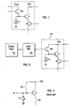
- Figure 3 shows a typical active-pixel sensor circuit.
- the gate of transistor N1 is connected to a reset switch RES and the cathode of a photodiode PD . Initially, the reset switch RES is open and the voltage at node IN approximates the voltage generated by the photodiode, V PD .
- select switch SEL When select switch SEL is closed, the voltage at node IN is read from the pixel circuit, less a threshold voltage V T .
- reset switch RES When reset switch RES is closed, the voltage at node IN rises to approximately V dd . The voltage at node IN is again read from the pixel circuit. Subtracting the two samples removes any noise which is common (or correlated) to both, leaving only the data signal.
- this approach does not suppress the mismatch effect caused by a non-ideal reset switch RES since the switch is outside of the double-sampling path.
- FIG. 1 shows a first embodiment for suppressing FPN from a non-ideal reset switch.
- the drain of the transistor reset switch RES is connected to a reset voltage source, V RES , which is independent of V dd .
- Voltage V RES should be set less than V dd by at least one V T , the threshold voltage, (including backgate bias effect) plus delta ( V T ) (the maximum V T variation for a given process), for all operational conditions (for example, a wide temperature range, bright-light sensing, and dark sensing).
- V RES V dd - (V T + delta(V T )).
- the gate of the reset transistor RES is switched between a low voltage and V dd to turn transistor RES OFF and ON, respectively.
- the gate voltage of transistor RES is approximately V dd
- transistor RES is operating in its linear region (the difference of V dd and V RES is at least one V T , which is sufficient to operate transistor RES in its linear region).
- the source or gate voltage of the pixel-sensing transistor N1 can be pulled up to the transistor RES drain voltage, V RES .
- the drain voltage is equal to V RES , no matter what the fabricated size of transistor RES, or the associated V T voltage variation.
- each of the pixel-sensing NMOS transistors N1 in a CMOS imager are able to sense the same V RES voltage during the reset phase, regardless of the variations in threshold voltages inherent across the large number of reset switches fabricated in the pixel circuits of the imager. Therefore the mismatch effect of the reset switching transistor RES is significantly reduced and hence FPN on the pixel readout is also significantly reduced.
- Figure 2 shows a second embodiment for suppressing FPN from a non-ideal reset switch.
- This approach connects the drain of the reset switching transistor RES to V dd (which is also connected to the drain of pixel-sensing transistor N1).
- V g of transistor RES is set higher than the V dd ; at least one V T (including backgate bias effect) plus delta(V T ) (the maximum V T variation for a given process), for all operational conditions (for example, a wide temperature range, bright-light sensing, and dark sensing).
- V gh the higher gate voltage, V gh , of the reset transistor RES is derived as follows, V gh > V dd + (V T + delta(V T )).
- a charge pump circuit 200 is added to obtain the higher gate voltage level, V gh .
- a level-shift circuit 204 is connected between the charge pump 200 and pixel circuits 204 to increase the input gate voltage level of transistor RES from V dd to V gh .
- all pixel-sensing transistors N1 in a CMOS imager are able to sense the exact same V dd voltage during the reset phase. Therefore the mismatch effect of the reset transistor RES will not produce FPN during readout of the pixel.
- the reset voltage V RES is derived independently of the supply voltage V dd , and consequently, an additional line is needed for the pixel circuit. Therefore the area of the pixel in the first approach is slightly larger than the area of the pixel in the second approach. Hence the optical fill factor (the percentage of area in the array actually used for sensing) in the first approach will be smaller than that in the second approach for pixels of equal size.
- both the charge pump 200 and level shift 204 circuits are implemented outside of the pixel circuit. Therefore a higher optical fill factor can be achieved than that of the first approach.
- the charge pump circuit 200 may not be required in a dual 3.3V/5V power supply CMOS process.
- the higher gate voltage, V gh can be set directly to be 5V while the V dd is 3.3V.
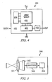
- Figure 4 shows an imager chip comprising the sampling architecture of the first or second embodiment.
- the chip 400 incorporates a row select circuitry 404 and column select circuitry 402 to read the array sensor 401.
- the output circuitry 403 receives pixel data from the column circuitry 402 and presents it to the output terminal OUT. Additional support circuit may be fabricated in the peripheral region 405.
- the chip 400 also has connections for supply voltage VDD, ground GND, and clocking signals CLOCK.
- Figure 5 shows a camera using an integrated circuit imaging chip using with the readout architecture of the first or second embodiment.
- the camera 500 has a lens 501 which focuses an image onto the image sensor chip 502.
- a processor 503 receives the data from the image chip 503 and sends it to a storage and output system 504.
- Embodiments of the invention may be modified or varied, for example as follows.
- circuit elements can be added to, or substituted into, the specific circuit topologies shown.
- Nonlinear devices can be added in series with (or used to replace) resistors, to increase the impedance of load devices.
- the apparatus and method can also be used in reduced voltage array architectures.
Landscapes
- Engineering & Computer Science (AREA)
- Multimedia (AREA)
- Signal Processing (AREA)
- Transforming Light Signals Into Electric Signals (AREA)
- Solid State Image Pick-Up Elements (AREA)
- Electronic Switches (AREA)
- Logic Circuits (AREA)
Applications Claiming Priority (2)
| Application Number | Priority Date | Filing Date | Title |
|---|---|---|---|
| US7022397P | 1997-12-31 | 1997-12-31 | |
| US70223P | 1997-12-31 |
Publications (2)
| Publication Number | Publication Date |
|---|---|
| EP0928101A2 true EP0928101A2 (fr) | 1999-07-07 |
| EP0928101A3 EP0928101A3 (fr) | 2001-05-02 |
Family
ID=22093951
Family Applications (1)
| Application Number | Title | Priority Date | Filing Date |
|---|---|---|---|
| EP98310649A Withdrawn EP0928101A3 (fr) | 1997-12-31 | 1998-12-23 | Matrice de capteurs CMOS |
Country Status (3)
| Country | Link |
|---|---|
| US (1) | US6618083B1 (fr) |
| EP (1) | EP0928101A3 (fr) |
| JP (1) | JPH11266404A (fr) |
Cited By (6)
| Publication number | Priority date | Publication date | Assignee | Title |
|---|---|---|---|---|
| EP0905788A3 (fr) * | 1997-09-29 | 2000-06-28 | Canon Kabushiki Kaisha | Capteur d'images de type MOS |
| EP1006718A3 (fr) * | 1998-12-01 | 2000-07-19 | Hewlett-Packard Company | Circuit de commande de pixels avec protection contre les surtensions |
| GB2347212A (en) * | 1999-02-24 | 2000-08-30 | Sharp Kk | Active type solid-state imaging device |
| EP1175084A3 (fr) * | 2000-07-21 | 2002-06-19 | Mitsubishi Denki Kabushiki Kaisha | Dispositif de prise d'images à semi-conducteur |
| FR2824664A1 (fr) * | 2001-05-09 | 2002-11-15 | St Microelectronics Sa | Photodetecteur cmos comportant une photodiode en silicium amorphe |
| DE102006031482A1 (de) * | 2005-08-01 | 2007-04-19 | Samsung Electro-Mechanics Co., Ltd., Suwon | CMOS-Bildsensor mit Dunkelstrom-Kompensationsfunktion |
Families Citing this family (38)
| Publication number | Priority date | Publication date | Assignee | Title |
|---|---|---|---|---|
| US7129978B1 (en) * | 1998-07-13 | 2006-10-31 | Zoran Corporation | Method and architecture for an improved CMOS color image sensor |
| US6825878B1 (en) * | 1998-12-08 | 2004-11-30 | Micron Technology, Inc. | Twin P-well CMOS imager |
| US7116366B1 (en) | 1999-08-31 | 2006-10-03 | Micron Technology, Inc. | CMOS aps pixel sensor dynamic range increase |
| US7176446B1 (en) | 1999-09-15 | 2007-02-13 | Zoran Corporation | Method and apparatus for distributing light onto electronic image sensors |
| US7053945B1 (en) * | 2000-07-26 | 2006-05-30 | Micron Technolopgy, Inc. | Image sensor having boosted reset |
| US6952226B2 (en) * | 2000-12-22 | 2005-10-04 | Texas Instruments Incorporated | Stray-insensitive, leakage-independent image sensing with reduced sensitivity to device mismatch and parasitic routing capacitance |
| TW474459U (en) * | 2001-01-19 | 2002-01-21 | Sunplus Technology Co Ltd | Active pixel sensor with reset transistor separated from voltage source of the other circuit |
| US6937278B2 (en) * | 2001-04-02 | 2005-08-30 | Micron Technology, Inc. | Row driver circuit for a sensor including a shared row-reset bus and a charge pump boosting circuit |
| WO2002091736A1 (fr) * | 2001-04-27 | 2002-11-14 | Honda Giken Kogyo Kabushiki Kaisha | Unite de correction de sortie d'un capteur d'image |
| US6795117B2 (en) * | 2001-11-06 | 2004-09-21 | Candela Microsystems, Inc. | CMOS image sensor with noise cancellation |
| US8054357B2 (en) * | 2001-11-06 | 2011-11-08 | Candela Microsystems, Inc. | Image sensor with time overlapping image output |
| US7233350B2 (en) * | 2002-01-05 | 2007-06-19 | Candela Microsystems, Inc. | Image sensor with interleaved image output |
| US7709777B2 (en) * | 2003-06-16 | 2010-05-04 | Micron Technology, Inc. | Pumps for CMOS imagers |
| GB2457851B (en) | 2006-12-14 | 2011-01-05 | Ion Torrent Systems Inc | Methods and apparatus for measuring analytes using large scale fet arrays |
| US11339430B2 (en) | 2007-07-10 | 2022-05-24 | Life Technologies Corporation | Methods and apparatus for measuring analytes using large scale FET arrays |
| US8262900B2 (en) | 2006-12-14 | 2012-09-11 | Life Technologies Corporation | Methods and apparatus for measuring analytes using large scale FET arrays |
| US20100137143A1 (en) | 2008-10-22 | 2010-06-03 | Ion Torrent Systems Incorporated | Methods and apparatus for measuring analytes |
| US20100301398A1 (en) | 2009-05-29 | 2010-12-02 | Ion Torrent Systems Incorporated | Methods and apparatus for measuring analytes |
| US8776573B2 (en) | 2009-05-29 | 2014-07-15 | Life Technologies Corporation | Methods and apparatus for measuring analytes |
| EP2588851B1 (fr) | 2010-06-30 | 2016-12-21 | Life Technologies Corporation | Circuit d'accumulation de charge sensible aux ions et procédé associé |
| TWI465716B (zh) | 2010-06-30 | 2014-12-21 | 生命技術公司 | 用於檢測及測量化學反應及化合物之電晶體電路 |
| EP2588850B1 (fr) | 2010-06-30 | 2016-12-28 | Life Technologies Corporation | Procédé de test à sec de réseaux d'isfet |
| US11307166B2 (en) | 2010-07-01 | 2022-04-19 | Life Technologies Corporation | Column ADC |
| US8653567B2 (en) | 2010-07-03 | 2014-02-18 | Life Technologies Corporation | Chemically sensitive sensor with lightly doped drains |
| WO2012036679A1 (fr) | 2010-09-15 | 2012-03-22 | Life Technologies Corporation | Procédés et appareil de mesure d'analytes |
| US8685324B2 (en) * | 2010-09-24 | 2014-04-01 | Life Technologies Corporation | Matched pair transistor circuits |
| US9970984B2 (en) | 2011-12-01 | 2018-05-15 | Life Technologies Corporation | Method and apparatus for identifying defects in a chemical sensor array |
| US9080968B2 (en) | 2013-01-04 | 2015-07-14 | Life Technologies Corporation | Methods and systems for point of use removal of sacrificial material |
| US9841398B2 (en) | 2013-01-08 | 2017-12-12 | Life Technologies Corporation | Methods for manufacturing well structures for low-noise chemical sensors |
| US8963216B2 (en) | 2013-03-13 | 2015-02-24 | Life Technologies Corporation | Chemical sensor with sidewall spacer sensor surface |
| CN105264366B (zh) | 2013-03-15 | 2019-04-16 | 生命科技公司 | 具有一致传感器表面区域的化学传感器 |
| US9835585B2 (en) | 2013-03-15 | 2017-12-05 | Life Technologies Corporation | Chemical sensor with protruded sensor surface |
| WO2014149779A1 (fr) | 2013-03-15 | 2014-09-25 | Life Technologies Corporation | Dispositif chimique à élément conducteur mince |
| US20140336063A1 (en) | 2013-05-09 | 2014-11-13 | Life Technologies Corporation | Windowed Sequencing |
| US10458942B2 (en) | 2013-06-10 | 2019-10-29 | Life Technologies Corporation | Chemical sensor array having multiple sensors per well |
| US10077472B2 (en) | 2014-12-18 | 2018-09-18 | Life Technologies Corporation | High data rate integrated circuit with power management |
| KR102593647B1 (ko) | 2014-12-18 | 2023-10-26 | 라이프 테크놀로지스 코포레이션 | 트랜스미터 구성을 갖춘 높은 데이터율 집적 회로 |
| US10004125B2 (en) * | 2015-05-22 | 2018-06-19 | Google Llc | Automatically adjust sensor sample rates and modes based on sensor feedback and system state |
Family Cites Families (11)
| Publication number | Priority date | Publication date | Assignee | Title |
|---|---|---|---|---|
| JPS5738073A (en) * | 1980-08-20 | 1982-03-02 | Hitachi Ltd | Solid-state image sensor |
| JPH05198755A (ja) * | 1991-08-29 | 1993-08-06 | Mitsubishi Electric Corp | 半導体論理回路 |
| JP2965777B2 (ja) * | 1992-01-29 | 1999-10-18 | オリンパス光学工業株式会社 | 固体撮像装置 |
| US6002432A (en) * | 1996-09-10 | 1999-12-14 | Foveon, Inc. | Method for operating an active pixel sensor cell that reduces noise in the photo information extracted from the cell |
| US6469740B1 (en) * | 1997-02-04 | 2002-10-22 | Matsushita Electric Industrial Co., Ltd. | Physical quantity distribution sensor and method for driving the same |
| US5969758A (en) * | 1997-06-02 | 1999-10-19 | Sarnoff Corporation | DC offset and gain correction for CMOS image sensor |
| TW421962B (en) * | 1997-09-29 | 2001-02-11 | Canon Kk | Image sensing device using mos type image sensing elements |
| US6246436B1 (en) * | 1997-11-03 | 2001-06-12 | Agilent Technologies, Inc | Adjustable gain active pixel sensor |
| US6369853B1 (en) * | 1997-11-13 | 2002-04-09 | Foveon, Inc. | Intra-pixel frame storage element, array, and electronic shutter method suitable for electronic still camera applications |
| US6046444A (en) * | 1997-12-08 | 2000-04-04 | Intel Corporation | High sensitivity active pixel with electronic shutter |
| US6476864B1 (en) * | 1998-05-11 | 2002-11-05 | Agilent Technologies, Inc. | Pixel sensor column amplifier architecture |
-
1998
- 1998-12-23 EP EP98310649A patent/EP0928101A3/fr not_active Withdrawn
- 1998-12-30 US US09/223,698 patent/US6618083B1/en not_active Expired - Lifetime
-
1999
- 1999-01-04 JP JP11000233A patent/JPH11266404A/ja active Pending
Cited By (13)
| Publication number | Priority date | Publication date | Assignee | Title |
|---|---|---|---|---|
| US6670990B1 (en) | 1997-09-29 | 2003-12-30 | Canon Kabushiki Kaisha | Image sensing device using MOS-type image sensing element whose threshold voltage of charge transfer switch and reset switch is different from that of signal output transistor |
| US6946637B2 (en) | 1997-09-29 | 2005-09-20 | Canon Kabushiki Kaisha | Image sensing device using MOS type image sensing elements |
| EP0905788A3 (fr) * | 1997-09-29 | 2000-06-28 | Canon Kabushiki Kaisha | Capteur d'images de type MOS |
| EP1006718A3 (fr) * | 1998-12-01 | 2000-07-19 | Hewlett-Packard Company | Circuit de commande de pixels avec protection contre les surtensions |
| US6784934B1 (en) | 1999-02-24 | 2004-08-31 | Sharp Kabushiki Kaisha | Active type solid-state imaging device with reduced pixel leak current |
| GB2347212B (en) * | 1999-02-24 | 2001-04-25 | Sharp Kk | Active type solid-state imaging device |
| GB2347212A (en) * | 1999-02-24 | 2000-08-30 | Sharp Kk | Active type solid-state imaging device |
| US6518559B2 (en) | 2000-07-21 | 2003-02-11 | Mitsubishi Denki Kabushiki Kaisha | Semiconductor image pickup device |
| EP1175084A3 (fr) * | 2000-07-21 | 2002-06-19 | Mitsubishi Denki Kabushiki Kaisha | Dispositif de prise d'images à semi-conducteur |
| FR2824664A1 (fr) * | 2001-05-09 | 2002-11-15 | St Microelectronics Sa | Photodetecteur cmos comportant une photodiode en silicium amorphe |
| EP1256984A3 (fr) * | 2001-05-09 | 2002-12-18 | STMicroelectronics S.A. | Photod-tecteur CMOS comportant une photodiode en silicium amorphe |
| US6831264B2 (en) | 2001-05-09 | 2004-12-14 | Stmicroelectronics S.A. | CMOS photodetector including an amorphous silicon photodiode and a saturation system |
| DE102006031482A1 (de) * | 2005-08-01 | 2007-04-19 | Samsung Electro-Mechanics Co., Ltd., Suwon | CMOS-Bildsensor mit Dunkelstrom-Kompensationsfunktion |
Also Published As
| Publication number | Publication date |
|---|---|
| US6618083B1 (en) | 2003-09-09 |
| JPH11266404A (ja) | 1999-09-28 |
| EP0928101A3 (fr) | 2001-05-02 |
Similar Documents
| Publication | Publication Date | Title |
|---|---|---|
| US6618083B1 (en) | Mismatch-independent reset sensing for CMOS area array sensors | |
| CN1833429B (zh) | 双转换增益成像器 | |
| US7728892B2 (en) | Image sensor with a capacitive storage node linked to transfer gate | |
| US6248991B1 (en) | Sequential correlated double sampling technique for CMOS area array sensors | |
| US7375748B2 (en) | Differential readout from pixels in CMOS sensor | |
| US10032825B2 (en) | Image sensor with a gated storage node linked to transfer gate | |
| US7825967B2 (en) | Column-wise clamp voltage driver for suppression of noise in an imager | |
| KR100965357B1 (ko) | 이미저에서의 잡음 감소 | |
| US8174601B2 (en) | Image sensor with controllable transfer gate off state voltage levels | |
| US7345269B2 (en) | Method and apparatus providing configurable current source device for image sensors with a selective current at an output node | |
| US7116367B2 (en) | Solid-state image pickup apparatus having a reset transistor controlled by an output line | |
| KR20070055545A (ko) | 화소 리셋 전압 부스팅 화소 | |
| JP2001268443A (ja) | Cmosイメージセンサーのアクティブピクセル回路 | |
| WO2004043078A1 (fr) | Capteur de pixel numerique avec commande anti-eblouissement | |
| US6697108B1 (en) | Fast frame readout architecture for array sensors with integrated correlated double sampling system | |
| US20050062866A1 (en) | Multiplexed pixel column architecture for imagers | |
| KR100775009B1 (ko) | 상관 이중 샘플링 회로 및 이를 구비한 시모스 이미지 센서 | |
| US7619671B2 (en) | Method, apparatus and system for charge injection suppression in active pixel sensors | |
| WO2002063691A2 (fr) | Cellule de pixel actif avec condensateur | |
| TWI897296B (zh) | 像素排列、成像裝置及用於操作像素排列之方法 | |
| EP0928102B1 (fr) | Capteurs matriciels |
Legal Events
| Date | Code | Title | Description |
|---|---|---|---|
| PUAI | Public reference made under article 153(3) epc to a published international application that has entered the european phase |
Free format text: ORIGINAL CODE: 0009012 |
|
| AK | Designated contracting states |
Kind code of ref document: A2 Designated state(s): DE FR GB IT NL |
|
| AX | Request for extension of the european patent |
Free format text: AL;LT;LV;MK;RO;SI |
|
| PUAL | Search report despatched |
Free format text: ORIGINAL CODE: 0009013 |
|
| AK | Designated contracting states |
Kind code of ref document: A3 Designated state(s): AT BE CH CY DE DK ES FI FR GB GR IE IT LI LU MC NL PT SE |
|
| AX | Request for extension of the european patent |
Free format text: AL;LT;LV;MK;RO;SI |
|
| RIC1 | Information provided on ipc code assigned before grant |
Free format text: 7H 04N 3/15 A, 7H 04N 5/217 B |
|
| 17P | Request for examination filed |
Effective date: 20011005 |
|
| 17Q | First examination report despatched |
Effective date: 20011127 |
|
| AKX | Designation fees paid |
Free format text: DE FR GB IT NL |
|
| STAA | Information on the status of an ep patent application or granted ep patent |
Free format text: STATUS: THE APPLICATION IS DEEMED TO BE WITHDRAWN |
|
| 18D | Application deemed to be withdrawn |
Effective date: 20021127 |