EP0928486B1 - Dispositif et procede d'essai des des d'un circuit integre dans un module de circuit integre - Google Patents
Dispositif et procede d'essai des des d'un circuit integre dans un module de circuit integre Download PDFInfo
- Publication number
- EP0928486B1 EP0928486B1 EP97938416A EP97938416A EP0928486B1 EP 0928486 B1 EP0928486 B1 EP 0928486B1 EP 97938416 A EP97938416 A EP 97938416A EP 97938416 A EP97938416 A EP 97938416A EP 0928486 B1 EP0928486 B1 EP 0928486B1
- Authority
- EP
- European Patent Office
- Prior art keywords
- circuit
- module
- test mode
- voltage
- function circuit
- Prior art date
- Legal status (The legal status is an assumption and is not a legal conclusion. Google has not performed a legal analysis and makes no representation as to the accuracy of the status listed.)
- Expired - Lifetime
Links
Images






Classifications
-
- G—PHYSICS
- G11—INFORMATION STORAGE
- G11C—STATIC STORES
- G11C29/00—Checking stores for correct operation ; Subsequent repair; Testing stores during standby or offline operation
-
- H—ELECTRICITY
- H10—SEMICONDUCTOR DEVICES; ELECTRIC SOLID-STATE DEVICES NOT OTHERWISE PROVIDED FOR
- H10P—GENERIC PROCESSES OR APPARATUS FOR THE MANUFACTURE OR TREATMENT OF DEVICES COVERED BY CLASS H10
- H10P74/00—Testing or measuring during manufacture or treatment of wafers, substrates or devices
- H10P74/23—Testing or measuring during manufacture or treatment of wafers, substrates or devices characterised by multiple measurements, corrections, marking or sorting processes
- H10P74/232—Testing or measuring during manufacture or treatment of wafers, substrates or devices characterised by multiple measurements, corrections, marking or sorting processes comprising connection or disconnection of parts of a device in response to a measurement
-
- G—PHYSICS
- G11—INFORMATION STORAGE
- G11C—STATIC STORES
- G11C29/00—Checking stores for correct operation ; Subsequent repair; Testing stores during standby or offline operation
- G11C29/04—Detection or location of defective memory elements, e.g. cell constructio details, timing of test signals
- G11C29/08—Functional testing, e.g. testing during refresh, power-on self testing [POST] or distributed testing
- G11C29/12—Built-in arrangements for testing, e.g. built-in self testing [BIST] or interconnection details
- G11C29/46—Test trigger logic
-
- G—PHYSICS
- G11—INFORMATION STORAGE
- G11C—STATIC STORES
- G11C29/00—Checking stores for correct operation ; Subsequent repair; Testing stores during standby or offline operation
- G11C29/70—Masking faults in memories by using spares or by reconfiguring
- G11C29/78—Masking faults in memories by using spares or by reconfiguring using programmable devices
- G11C29/785—Masking faults in memories by using spares or by reconfiguring using programmable devices with redundancy programming schemes
-
- G—PHYSICS
- G11—INFORMATION STORAGE
- G11C—STATIC STORES
- G11C29/00—Checking stores for correct operation ; Subsequent repair; Testing stores during standby or offline operation
- G11C29/70—Masking faults in memories by using spares or by reconfiguring
- G11C29/78—Masking faults in memories by using spares or by reconfiguring using programmable devices
- G11C29/80—Masking faults in memories by using spares or by reconfiguring using programmable devices with improved layout
-
- G—PHYSICS
- G11—INFORMATION STORAGE
- G11C—STATIC STORES
- G11C29/00—Checking stores for correct operation ; Subsequent repair; Testing stores during standby or offline operation
- G11C29/70—Masking faults in memories by using spares or by reconfiguring
- G11C29/78—Masking faults in memories by using spares or by reconfiguring using programmable devices
- G11C29/80—Masking faults in memories by using spares or by reconfiguring using programmable devices with improved layout
- G11C29/808—Masking faults in memories by using spares or by reconfiguring using programmable devices with improved layout using a flexible replacement scheme
-
- G—PHYSICS
- G01—MEASURING; TESTING
- G01R—MEASURING ELECTRIC VARIABLES; MEASURING MAGNETIC VARIABLES
- G01R31/00—Arrangements for testing electric properties; Arrangements for locating electric faults; Arrangements for electrical testing characterised by what is being tested not provided for elsewhere
- G01R31/28—Testing of electronic circuits, e.g. by signal tracer
- G01R31/2851—Testing of integrated circuits [IC]
- G01R31/2884—Testing of integrated circuits [IC] using dedicated test connectors, test elements or test circuits on the IC under test
-
- H—ELECTRICITY
- H04—ELECTRIC COMMUNICATION TECHNIQUE
- H04J—MULTIPLEX COMMUNICATION
- H04J2203/00—Aspects of optical multiplex systems other than those covered by H04J14/05 and H04J14/07
- H04J2203/0001—Provisions for broadband connections in integrated services digital network using frames of the Optical Transport Network [OTN] or using synchronous transfer mode [STM], e.g. SONET, SDH
- H04J2203/0062—Testing
Definitions
- This invention relates to an integrated circuit module having a module terminal for receiving a first voltage from circuitry external to the module; an integrated circuit die having a bond pad and a function circuit.
- the invention also relates to a method for initiating a test mode and an operational mode in a function circuit in an integrated circuit die in an integrated circuit module.
- Integrated circuit (IC) dice are typically tested before they are packaged to determine if they have any failing circuitry.
- one of the first steps in testing a die is to initiate a test mode in the die by applying control signals to selected bond pads on the die referred to as test bond pads.
- test bond pads selected bond pads on the die referred to as test bond pads.
- DRAM Dynamic Random Access Memory
- OE Output Enable
- test bond pads 14 e.g., their OE bond pads
- reference voltage bond pads 16 to the reference voltage V ss through module terminals 18 to ensure that a test mode cannot be accidentally initiated in an end user's system. While this works well to prevent accidental initiation of a test mode in dice in an IC module in the field, unfortunately it also prevents intentional testing of the dice by an IC manufacturer after they are packaged in the IC module.
- US-A-5 305 267 describes a semiconductor memory device (SRAM).
- SRAM semiconductor memory device
- a pulse signal having a pulse width exceeding a predetermined time length is applied through a terminal.
- a pulse width detecting circuit detects the pulse width of the applied pulse signal to provide a holding signal.
- a test mode signal holding circuit holds an externally applied test mode request signal in response to the holding signal.
- pulse width detecting circuit is disabled by a fusion of a fuse, whereby the test mode operation is prevented from undesirably occurring.
- US-A-5,663,902 describes a programmable fuse circuit with a disabling static current path.
- the fuse logic circuit includes a controllable switch, load device, and at least one fuse, all of which are connected in a series so as to share a static current path.
- the controllable switch can be selectively controlled to enable or disable the current path of the programmable fuse circuit.
- the invention provides an integrated circuit module with the characterizing features of claim 1 and a method with the characterizing features of claim 14.
- An inventive integrated circuit (IC) module such as a Multi-Chip Module (MCM) includes a terminal receiving a test mode initiate signal, such as a supply voltage V cc , and an IC die having a bond pad and a function circuit.
- a switching apparatus such as a fuse, is connected with the bond pad between the terminal and the function circuit to conduct the test mode initiate signal to the function circuit, and an impedance apparatus, such as a resistor, connected between the function circuit and an operational mode signal, such as a reference voltage V ss , supports a difference in voltages between the test mode initiate signal at the function circuit and the operation mode signal.
- the function circuit responds to the test mode initiate signal by initiating a test mode in the die.
- the switching circuit also selectively isolates the function circuit from the die, and the impedance apparatus then conducts the operational mode signal to the function circuit.
- the function circuit responds to the operational mode signal by entering an operational mode.
- a test mode can be initiated in the die after it is packaged in the IC module by providing the test mode initiate signal at the terminal, and the test mode can then be disabled and the die fixed in the operational mode by selectively isolating the function circuit from the terminal with the switching apparatus, thereby ensuring that the test mode is not accidentally initiated by an end user in the field.
- the switching apparatus and the impedance apparatus are both incorporated in the die. and in other versions one or both of the switching apparatus and impedance apparatus are incorporated in a substrate of the IC module.
- the IC module itself is incorporated into an electronic system, such as a computer system.
- the operational mode signal is provided by an operational mode signal circuit on the die. or is provided by external circuitry through another terminal in the IC module.
- the test mode initiate signal is generated on the die by a test mode initiate signal circuit responsive to external circuitry rather than being provided by external circuitry.
- an IC module in another embodiment, includes one or more terminals receiving a test mode initiate signal and an operational mode signal.
- One or more IC dice in the IC module each have one or more function circuits and a plurality of bond pads, and a first subset of the bond pads is coupled to the function circuits while a second subset of the bond pads is adapted to receive signals other than the test mode initiate signal in the test mode.
- a dedicated conduction circuit coupled between the terminals and the first subset bond pads and isolated from the second subset bond pads conducts the test mode initiate and operational mode signals to the function circuits.
- a test mode can be initiated in the dice after they are packaged in the IC module by providing the test mode initiate signal at the terminals, and an operational mode can be initiated by providing the operational mode signal at the terminals.
- the IC module is incorporated into an electronic system.
- the terminals comprise a first terminal receiving the test mode initiate signal and a second terminal receiving the operational mode signal, and the first and second terminals are coupled by an impedance element, such as a resistor, or by a link, such as a surface mount resistor or a jumper.
- a test apparatus for testing dice provided in one of the inventive IC modules described above includes a test-apparatus-to-module interface coupleable to terminals of the IC module.
- a test mode initiate circuit initiates a test mode in the dice by providing the test mode initiate signal through the interface, and a test signal circuit for testing the dice in the test mode provides test signals to the dice through the interface.
- a response signal circuit receives response signals through the interface from the dice in response to the test signals, and an evaluator circuit evaluates the response signals to identify any failing elements in the dice.
- the functionality of the embodiment is incorporated into a computer test device including a test-device-to-module interface, an input/output device coupled to the interface for receiving signals from and outputting signals to the dice, a memory device, and a processor.
- a method for initiating a test mode and an operational mode in dice in an IC module includes: receiving a test mode initiate signal at a terminal of the IC module; conducting the test mode initiate signal only to those bond pads on dice in the IC module adapted to receive the signal and from those bond pads to function circuits in the dice to initiate a test mode therein; discontinuing conduction of the test mode initiate signal to the function circuits; and conducting an operational mode initiate signal to each function circuit to initiate the operational mode therein.
- a method for testing one or more dice in an IC module includes: providing a test mode initiate signal to an externally accessible terminal of the IC module; conducting the test mode initiate signal exclusively to bond pads on the dice adapted to receive the signal to initiate a test mode in the dice; testing each die; receiving response signals from the dice; and evaluating the response signals to identify any failing elements in the dice.
- the method also includes: determining an address associated with each failing element; latching the failing element's address into the dice; providing a programming mode enable signal, such as a super voltage CAS signal, to the dice to enable a programming mode therein; enabling a redundant element in one of the dice to replace a failing element; and programming a redundancy circuit associated with the enabled redundant element to store the failing element's address so that the stored address directs the redundancy circuit to replace the failing element with the enabled redundant element.
- a programming mode enable signal such as a super voltage CAS signal
- Another embodiment of the present invention is a computer readable storage medium upon which is stored a program for controlling a computer to perform in accordance with the method described above for testing one or more dice in an IC module.
- an inventive integrated circuit (IC) module 20 includes IC dice 22 having function circuits, such as input buffers 24, selectively receiving a test mode initiate signal, such as a supply voltage V cc , through a module terminal 26, a switching circuit 28, and test mode enable bond pads 30 (e.g., Output Enable (OE) bond pads).
- a test mode initiate signal such as a supply voltage V cc
- module terminal 26 e.g., a test mode initiate signal
- test mode enable bond pads 30 e.g., Output Enable (OE) bond pads
- the IC module 20 may be any electronic structure having at least one die accessed externally through terminals, including, for example, any Multi-Chip Module (MCM), such as a Single In-line Memory Module (SIMM), a Dual In-line Memory Module (DIMM), a Random Access Memory (RAM) card, a flash Read-Only-Memory (ROM) module or card, a Synchronous Dynamic RAM (SDRAM) module or card, and a Rambus RAM module or card.
- MCM Multi-Chip Module
- SIMM Single In-line Memory Module
- DIMM Dual In-line Memory Module
- RAM Random Access Memory
- ROM flash Read-Only-Memory
- SDRAM Synchronous Dynamic RAM
- the dice 22 may be any dice for purposes of the present invention, including, for example, DRAM dice, Static Random Access Memory (SRAM) dice, Synchronous Graphics Random Access Memory (SGRAM) dice, ROM dice, and processor dice.
- the function circuits may be any circuitry on a die for initiating a test mode in the die
- the test mode initiate signal may be any signal for initiating a test mode in a die
- the module terminal 26 may be any terminal including, for example, a MCM pin (e.g., a SIMM, DIMM, RAM card, RAM module, ROM card, or ROM module pin)
- the switching circuit 28 may be, for example, a fuse or a transistor or any other device for selectively isolating the function circuits from the module terminal 26, and the test mode enable bond pads 30 may be any bond pads connectable to a function circuit for enabling a test mode in a die.
- the switching circuit 28 is shown in FIG. 2 as being a single circuit coupled to the module terminal 26, it may instead comprise a plurality of circuits, each one coupled to the module terminal 26 and one of the dice 22.
- the input buffers 24 In response to receiving the test mode initiate signal, the input buffers 24 initiate a test mode in the dice 22. In this mode, various test signals may be provided to the dice 22 in a well known manner to test the circuitry thereon, and the dice 22 then output various response signals indicating the presence of any failing circuitry.
- an impedance circuit 32 such as, for example, a resistor, resistance-connected MOS transistor, or anti-fuse, supports a difference in voltages between the test mode initiate signal at the test mode enable bond pads 30 and an operational mode enable signal, such as a reference voltage V ss , at a reference terminal 34, such as, for example, a MCM pin (e.g., a SIMM, DIMM, RAM card, RAM module, ROM card, or ROM module pin).
- a MCM pin e.g., a SIMM, DIMM, RAM card, RAM module, ROM card, or ROM module pin.
- the impedance circuit 32 is shown in FIG. 2 as being a single circuit coupled to the reference terminal 34, it may instead comprise a plurality of circuits, each one coupled to the reference terminal 34 and one of the dice 22.
- the switching circuit 28 isolates the input buffers 24 from the module terminal 26 to disable the test mode, and the impedance circuit 32 conducts the operational mode signal, such as the reference voltage V ss , to the input buffers 24.
- the input buffers 24 initiate an operational mode in the dice 22 in which the dice 22 operate in accordance with their intended normal function.
- the dice 22 are DRAMs, they would perform normal memory operations in their operational mode.
- the dice 22 in the IC module 20 are fully testable even after being packaged, and yet their test mode can be disabled as necessary so the IC module 20 can be used by end users in the field.
- one or both of the switching circuit 28 and the impedance circuit 32 may be incorporated into the dice 22 instead of being provided on a substrate 36 of the IC module 20 as shown in FIG. 2. Also, as will be described in more detail below with respect to FIG. 9, one or both of the test mode initiate signal and the operational mode signal may be generated on the dice 22 rather than being provided by external circuitry.
- the switching circuit 28 of FIG. 2 can be, for example, a fuse 38 that is blown once testing is complete, or an NMOS transistor 40 or PMOS transistor 42 that is de-activated once testing is complete.
- the impedance circuit 32 of FIG. 2 can be, for example, a resistor 44, an anti-fuse 46 that is blown once testing is complete, or an NMOS transistor 48 that is activated once testing is complete.
- 4C may be controlled by an anti-fuse isolate logic circuit 50 that outputs a high voltage during a test mode and is then programmed to output a low voltage once testing is complete.
- the high voltage during the test mode activates the NMOS transistor 40 and de-activates the NMOS transistor 48 through an inverter 52, and the low voltage after programming de-activates the NMOS transistor 40 and activates the NMOS transistor 48 through the inverter 52.
- an anti-fuse isolate logic circuit 50 that outputs a high voltage during a test mode and is then programmed to output a low voltage once testing is complete.
- the high voltage during the test mode activates the NMOS transistor 40 and de-activates the NMOS transistor 48 through an inverter 52, and the low voltage after programming de-activates the NMOS transistor 40 and activates the NMOS transistor 48 through the inverter 52.
- the present invention comprises an electronic system 60, such as a computer system, including an input device 62, an output device 64, a processor device 66, such as a state machine, and a memory device, such as an IC module 68.
- an electronic system 60 such as a computer system
- the input device 62 an output device 64
- a processor device 66 such as a state machine
- a memory device such as an IC module 68.
- the IC module 68 could comprise all or any portion of the input device 62, the output device 64, the processor device 66, and the memory device.
- the electronic system 60 will be described with respect to a particular IC module 68, it will be understood that the present invention includes any of the inventive IC modules described herein as incorporated into an electronic system.
- the IC module 68 may comprise any electronic structure having at least one die externally accessible through terminals, including, for example, a MCM, such as a SIMM, DIMM, RAM card, RAM module, ROM card, or ROM module.
- a MCM such as a SIMM, DIMM, RAM card, RAM module, ROM card, or ROM module.
- the IC module 68 includes a terminal 70, such as a MCM pin as discussed above, receiving a test mode initiate signal (e.g., the supply voltage V cc ) from the processor device 66.
- the terminal 70 conducts the test mode initiate signal to a bond pad 72 of an IC die 74.
- the IC die 74 may be any die, including, for example, a DRAM die, SRAM die, SGRAM die, processor die, flash ROM die, SDRAM die, or Rambus RAM die.
- a switching circuit 76 conducts the test mode initiate signal from the bond pad 72 to a function circuit 78 (e.g., an OE input buffer).
- the function circuit 78 initiates a test mode in the die 74 as described above. While the test mode initiate signal is being conducted to the function circuit 78, an impedance circuit 80 supports a difference in voltages between the test mode initiate signal at the function circuit 78 and an operational mode signal, such as a reference voltage V ss , supplied by an operational mode voltage circuit 82.
- the switching circuit 76 may, for example, comprise a fuse or a MOS transistor
- the function circuit 78 may comprise any circuit which enables or initiates a test mode in response to a test mode initiate signal
- the impedance circuit 80 may, for example, comprise an anti-fuse, a MOS transistor, or a resistor
- the operational mode voltage circuit 82 may comprise any circuit for supplying an operational mode signal, such as a reference voltage V ss , on a die.
- the switching circuit 76 isolates the function circuit 78 from the bond pad 72 to disable the test mode in the die 74 by, for example, blowing a fuse or de-activating a MOS transistor.
- the impedance circuit 80 then conducts the operational mode signal from the operational mode voltage circuit 82 to the function circuit 78 by, for example, blowing an anti-fuse or activating a MOS transistor.
- the function circuit 78 initiates an operational mode in the die 74 as described above.
- the die 74 is fully testable even after being packaged in the IC module 68, and yet the test mode of the die 74 can be disabled as necessary so the IC module 68 can be used by end users in the field.
- an inventive IC module 84 includes dice 86 having function circuits, such as input buffers 88, selectively receiving a test mode initiate signal, such as a supply voltage V cc , through a first terminal 90, a dedicated conductor 92, and test mode enable bond pads 94 (e.g., Output Enable (OE) bond pads).
- a test mode initiate signal such as a supply voltage V cc
- test mode enable bond pads 94 e.g., Output Enable (OE) bond pads.
- the IC module 84 may be any electronic structure having at least one die accessed externally through terminals, including, for example, a MCM, such as a SIMM, a DIMM, a RAM card, a RAM module, a ROM card, and a ROM module.
- the dice 86 may be any dice for purposes of the present invention, including, for example, DRAM dice, SRAM dice, SGRAM dice, flash ROM dice, SDRAM dice, Rambus RAM dice, and processor dice.
- the function circuits may be any circuitry on a die for initiating a test mode in the die
- the test mode initiate signal may be any signal for initiating a test mode in a die
- the first terminal 90 may be any terminal including, for example, a MCM pin, such as a SIMM, DIMM, RAM card, ROM card, RAM module, or ROM module pin
- the dedicated conductor 92 may be, for example, any conductive structure or device connected exclusively to those bond pads 94 on the dice 86 adapted to receive the test mode initiate signal or unaffected by receipt of the test mode initiate signal
- the test mode enable bond pads 94 may be any bond pads connectable to a function circuit for enabling a test mode in a die.
- the input buffers 88 In response to receiving the test mode initiate signal, the input buffers 88 initiate a test mode in the dice 86 in a well known manner as described above.
- an operational mode signal such as a reference voltage V ss , is provided through the first terminal 90 and the dedicated conductor 92 to the input buffers 88 to initiate an operational mode in the dice 86 in the well known manner described above.
- a second terminal 96 provides the reference voltage V ss to other circuits in the dice 86 via a reference conductor 97 and reference voltage bond pads 98.
- the dice 86 in the IC module 84 are fully testable even after being packaged, and yet the operational mode can be enabled as necessary so the IC module 86 can be used by end users in the field.
- a conductive via 100 through a substrate 102 of the IC module 84 couples the first terminal 90 and dedicated conductor 92 to the second terminal 96 and the reference conductor 97 through an impedance element, such as a surface mount resistor 104.
- an impedance element such as a surface mount resistor 104.
- the impedance element may, for example, comprise a resistance-connected MOS transistor rather than the surface mount resistor 104.
- a test mode initiate signal such as the supply voltage V cc
- an operational mode signal such as the reference voltage V ss
- V ss the reference voltage
- the operational mode signal may be supplied to the first terminal 90.
- the surface mount resistor 104 conducts the operational mode signal from the second terminal 96 to the dedicated conductor 92, in order to initiate the operational mode as described above with respect to FIG. 7.
- a test mode initiate signal such as the supply voltage V cc
- V cc the supply voltage
- an operational mode signal such as the reference voltage V ss
- V ss the reference voltage
- the operational mode signal may be supplied to the first terminal 90.
- the link 106 is positioned to connect the second terminal to the dedicated conductor 92 through the conductive via 100 in the substrate 102, thereby conducting the operational mode signal from the second terminal 96 to the dedicated conductor 92 in order to initiate the operational mode as described above with respect to FIG. 7.
- first and second terminals 90 and 96 are shown in FIG.'s 8A and 8B as being on opposing sides of the substrate 102, it will be understood that the invention is not so limited.
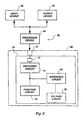
- the present invention comprises an IC die 108.
- the IC die 108 may be any die including, for example, a DRAM die, SRAM die, SGRAM die, flash ROM die, SDRAM die, Rambus RAM die, or processor die.
- a test mode enable signal directs a test mode voltage circuit 110 in the die 108 to generate a test mode voltage V TEST , such as 3.3 Volts.
- a switching circuit 112 then conducts the test mode voltage V TEST to a function circuit 114 (e.g., an OE input buffer).
- the function circuit 114 initiates a test mode in the die 108 as described above.
- an impedance circuit 116 supports a difference in voltages between the test mode voltage V TEST at the function circuit 114 and an operational mode voltage V OPER , such as 0.0 Volts, supplied by an operational mode voltage circuit 118.
- the switching circuit 112 may, for example, comprise a fuse or a MOS transistor
- the function circuit 114 may comprise any circuit which enables or initiates a test mode in response to a test mode voltage V TEST
- the impedance circuit 116 may, for example, comprise an anti-fuse, a MOS transistor, or a resistor
- the operational mode voltage circuit 118 may comprise any circuit for supplying an operational mode voltage V OPER on a die.
- the switching circuit 112 isolates the function circuit 114 from the test mode voltage V TEST to disable the test mode in the die 108 by, for example, blowing a fuse or de-activating a MOS transistor.
- the impedance circuit 116 then conducts the operational mode voltage V OPER from the operational mode voltage circuit 118 to the function circuit 114 by, for example, blowing an anti-fuse or activating a MOS transistor.
- the function circuit 118 initiates an operational mode in the die 108 as described above.
- the die 108 is fully testable even after being packaged, and yet the test mode of the die 108 can be disabled as necessary so the die 108 can be used by end users in the field.
- a test apparatus 120 for testing an IC module 122 of the present invention having an IC die 124 includes a test-apparatus-to-module interface 126 having interface terminals 128 connectable to module terminals 130 on the IC module 122.
- the module terminals 130 are in communication with the die 124 including a redundancy circuit 132.
- a test mode enable circuit 134 provides a test mode initiate signal to the die 124 through the interface 126 to initiate a test mode in the die 124 in the manner described above.
- a test signal circuit 136 then provides test signals to the die 124 through the interface 126 to test the die 124 in the test mode.
- a response signal circuit 138 receives response signals from the die 124 in the test mode in response to the test signals, and an evaluator circuit 140 then evaluates the response signals to identify any failing circuitry in the die 124.
- a repair enablement device 142 in the test apparatus 120 may provide repair control signals to the redundancy circuit 132 in the die 124 directing the redundancy circuit 132 to replace any failing circuitry identified by the evaluator circuit 140 with redundant elements 144 in the die 124.
- the manner in which repair control signals may direct the redundancy circuit 132 to repair any failing circuitry in the die 124 is well known by those skilled in the art.
- a processor 146 coupled to a memory device 148 and an input/output device 150 may provide the test mode initiate signal, the test signals, and the repair control signals, and may receive and evaluate the response signals, in the manner described above with respect to FIG. 10.
- the memory device 148 may comprise any permanent or temporary electronic storage medium, including, for example, a DRAM, SRAM, SGRAM, disk, tape, memory card, memory module, or programmable logic array.
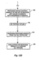
- a method for testing any one of the above-described inventive IC dice or modules includes the steps of: 160 providing a test mode initiate signal to an externally accessible terminal of an IC module; 162 conducting the test mode initiate signal exclusively to bond pads on dice in the IC module adapted to receive the signal to initiate a test mode in the dice; 164 testing each of the dice in the test mode by providing test signals to each die through the externally accessible terminals of the IC module; 166 receiving response signals from each die through the terminals of the IC module in response to the test signals; 168 evaluating the response signals from each die to identify any failing elements in the dice of the IC module; 170 providing repair control signals to a redundant circuit in each die to direct each die to replace any identified failing elements with redundant elements; 172 re-testing each die by providing re-test signals to each die through the IC module's externally accessible terminals; 174 receiving response signals from each die through the IC module's terminals
- the step 170 from FIGS. 12A and 12B of providing repair control signals to a redundant circuit in each die includes, for each identified failing element, the steps of: 180 determining an address associated with the failing element; 182 latching the failing element's address into the dice; 184 providing a programming mode enable signal, such as a super voltage Column Address Strobe (CAS) signal, to the dice to enable a programming mode therein; 186 applying a fuse address of a fusebank enable anti-fuse associated with a redundant element selected to replace the failing element to the IC module's terminals to identify the location of the anti-fuse; 188 coupling to the anti-fuse; 190 determining the anti-fuse's resistance; 192 applying a programming voltage, such as 8 to 10 Volts, to the anti-fuse to blow the anti-fuse; 194 re-determining the anti-fuse's resistance to confirm it is blown; and, for each asserted address bit in each failing element's address:
- any or all of the steps 160-206 in the embodiment of FIGS. 12A, 12B, 13A, and 13B, or any portion thereof, may be implemented in hardware, software, or both, using a wide variety of well-known architectures, including, for example, a state machine and the embodiment of FIGS. 10 and 11. It will also be understood that, although the embodiment of FIGS. 12A, 12B, 13A, and 13B has been described with respect to anti-fuses, any programmable circuit or element will work for purposes of the present invention. Also, it will be understood that the step 186 in FIG. 13A may include automatic selection of the location and type of redundant element (e.g., redundant row or column) to be used to replace the failing element. Finally, it will be understood that the steps 180 to 206 of FIG.'s 13A and 13B may be automated by computer or performed manually.
- redundant element e.g., redundant row or column
- the present invention thus advantageously provides a device and method for testing and repairing IC dice already packaged in IC modules.
Landscapes
- Semiconductor Integrated Circuits (AREA)
- Tests Of Electronic Circuits (AREA)
- Testing Or Measuring Of Semiconductors Or The Like (AREA)
Claims (21)
- Module (20) de circuit intégré possédant :une borne de module (26) destinée à recevoir une première tension de la part d'un circuit extérieur au module (20) ;une puce (22) de circuit intégré possédant un plot de liaison (30) et un circuit de fonction (24) ;ledit module de circuit intégré (20) étant caractérisé par un appareil servant à faire commuter ladite première tension sur ledit circuit de fonction (24) de ladite puce de circuit intégré (22) et à faire commuter une deuxième tension sur ledit circuit de fonction (24), ledit appareil comprenant :un circuit de commutation (28) connecté audit plot de liaison (30) entre ladite borne de module (26) et ledit circuit de fonction (24) afin d'isoler sélectivement ledit circuit de fonction (24) vis-à-vis de ladite borne de module (26) et, sinon, de conduire ladite première tension audit circuit de fonction (24) ; etun circuit d'impédance (32) servant à conduire ladite deuxième tension audit circuit de fonction (24) lorsque ledit circuit de fonction est isolé vis-à-vis de ladite borne de module (26) et, sinon, à supporter une différence de tension entre ladite première tension, présente sur ledit circuit de fonction, et ladite deuxième tension.
- Module de circuit intégré selon la revendication 1, où la première tension est une tension d'alimentation et la deuxième tension est une tension de référence.
- Module de circuit intégré selon la revendication 1, où le circuit de commutation (28) comprend un circuit programmable destiné à isoler, de manière programmable, le circuit de fonction (24).
- Module de circuit intégré selon la revendication 3, où le circuit programmable comprend un élément programmable sélectionné dans un groupe comprenant un fusible de métal et un fusible de silicium polycristallin.
- Module de circuit intégré selon la revendication 4, où l'élément programmable s'interpose entre le plot de liaison (30) du circuit de fonction (24) et la borne de module (26).
- Module de circuit intégré selon la revendication 1, où le circuit de commutation (28) comprend un élément commutable sélectionné dans un groupe comprenant un transistor NMOS et un transistor PMOS.
- Module de circuit intégré selon la revendication 1, où le circuit de commutation (28) disposé dans la puce et est connecté entre le plot de liaison (30) et le circuit de fonction (24).
- Module de circuit intégré selon la revendication 1, où le module (20) comporte un substrat auquel la puce est attachée, le circuit de commutation étant disposé dans le substrat et étant connecté entre la borne de module et le plot de liaison.
- Module de circuit intégré selon la revendication 1, où le circuit d'impédance (32) comprend un circuit de résistance sélectionné dans un groupe comprenant une résistance, un transistor MOS et un antifusible.
- Module de circuit intégré selon la revendication 1, où le circuit d'impédance (32) est disposé dans la puce et est connecté au plot de liaison (30) et au circuit de fonction (24).
- Module de circuit intégré selon la revendication 1, où le module comporte un substrat auquel la puce est attachée, le circuit d'impédance (32) étant disposé dans le substrat et étant connecté au plot de liaison (30).
- Module de circuit intégré selon la revendication 1, où le module possède également une borne de tension destinée à recevoir la deuxième tension de la part du circuit extérieur au module, le circuit d'impédance étant connecté entre la borne de tension et le plot de liaison.
- Module de circuit intégré selon la revendication 1, où la puce comporte un circuit d'alimentation destiné à produire la deuxième tension, le circuit d'impédance étant couplé entre le circuit d'alimentation et le circuit de fonction.
- Procédé permettant de faire démarrer un mode d'essai et un mode de fonctionnement dans un circuit de fonction qui se trouve dans une puce de circuit intégré d'un module de circuit intégré, le procédé étant caractérisé par les opérations suivantes :produire un module de circuit intégré qui possède une borne de module destinée à recevoir une première tension de la part d'un circuit extérieur au module, ledit module comprenant en outre :une puce de circuit intégré possédant un circuit de fonction ;un appareil servant à faire commuter ladite première tension sur ledit circuit de fonction de ladite puce de circuit intégré et à faire commuter une deuxième tension sur ledit circuit de fonction,ledit appareil comprenant :un circuit de commutation connecté à ladite borne de module et audit circuit de fonction afin d'isoler sélectivement ledit circuit de fonction vis-à-vis de ladite borne de module et, sinon, de conduire ladite première tension audit circuit de fonction ; etun circuit d'impédance servant à conduire ladite deuxième tension audit circuit de fonction lorsque ledit circuit de fonction est isolé vis-à-vis de ladite borne de module et, sinon, à supporter une différence de tension entre ladite première tension présente sur ledit circuit de fonction et ladite deuxième tension ;émettre un signal de démarrage de mode d'essai à destination de ladite borne de module ;conduire ledit signal de démarrage de mode d'essai audit circuit de fonction afin de faire démarrer le mode d'essai dans celui-ci ;interrompre la conduction du signal de démarrage de mode d'essai à destination dudit circuit de fonction ; etconduire le signal de démarrage du mode de fonctionnement audit circuit de fonction afin de faire démarrer le mode de fonctionnement dans celui-ci.
- Procédé selon la revendication 14, où l'opération consistant à conduire le signal de démarrage de mode d'essai comprend les opérations suivantesconnecter, de façon déconnectable, la borne de module audit circuit de fonction via un plot de liaison destiné à recevoir le signal de démarrage de mode d'essai ; etsupporter la différence des tensions entre le signal de démarrage de mode d'essai existant au niveau dudit circuit de fonction et le signal de démarrage de mode de fonctionnement.
- Procédé selon la revendication 15, où l'opération consistant à interrompre la conduction du signal de démarrage de mode d'essai à destination dudit circuit de fonction comprend la déconnexion dudit circuit de fonction vis-à-vis de la borne de module.
- Procédé selon la revendication 16, où l'opération consistant à déconnecter ledit circuit de fonction vis-à-vis de la borne de module comprend la programmation d'un élément programmable choisi dans un groupe comprenant un fusible et un antifusible.
- Procédé selon la revendication 14, où l'opération consistant à conduire le signal de démarrage de mode de fonctionnement à destination du circuit de fonction comprend les opérations suivantes ;prévoir une borne de fonctionnement dans le module ;recevoir le signal de démarrage de mode de fonctionnement sur la borne de fonctionnement ; etcouper la borne de fonctionnement audit circuit de fonction par l'intermédiaire d'un élément choisi dans le groupe comprenant ledit circuit d'impédance et une liaison.
- Procédé selon la revendication 14, où l'opération consistant à conduire le signal de démarrage de mode de fonctionnement à destination dudit circuit de fonction comprend les opérations suivantes :produire le signal de démarrage de mode de fonctionnement sur ladite puce ; etconduire le signal de démarrage de mode de fonctionnement ainsi produit à destination dudit circuit de fonction par l'intermédiaire dudit circuit d'impédance.
- Procédé selon la revendication 14, où ledit module de circuit intégré possède une pluralité de bornes accessibles depuis l'extérieur, ledit circuit de fonction étant du type pouvant passer dans le mode d'essai et le mode de fonctionnement en réponse à la réception de signaux respectifs de démarrage de mode d'essai et de démarrage de mode de fonctionnement, le procédé comprenant en outre les opérations suivantes :conduire, de manière déconnectable, le signal de démarrage de mode d'essai à destination du circuit de fonction afin de faire démarrer le mode d'essai dans celui-ci ; etdéconnecter le signal de démarrage de mode d'essai vis-à-vis du circuit de fonction.
- Procédé selon la revendication 14, où ladite puce comporte au moins un plot de liaison, ledit procédé comprenant en outre l'opération qui consiste à conduire le signal de démarrage de mode d'essai à destination desdits plots de liaison, lesquels sont destinés à recevoir le signal de démarrage de mode d'essai, et desdits plots de liaison à chaque dit circuit de fonction, afin de faire démarrer le mode d'essai dans celui-ci.
Applications Claiming Priority (3)
| Application Number | Priority Date | Filing Date | Title |
|---|---|---|---|
| US718173 | 1985-04-01 | ||
| US08/718,173 US5796746A (en) | 1995-12-22 | 1996-09-19 | Device and method for testing integrated circuit dice in an integrated circuit module |
| PCT/US1997/014564 WO1998012706A1 (fr) | 1996-09-19 | 1997-08-20 | Dispositif et procede d'essai des des d'un circuit integre dans un module de circuit integre |
Publications (2)
| Publication Number | Publication Date |
|---|---|
| EP0928486A1 EP0928486A1 (fr) | 1999-07-14 |
| EP0928486B1 true EP0928486B1 (fr) | 2001-11-14 |
Family
ID=24885103
Family Applications (1)
| Application Number | Title | Priority Date | Filing Date |
|---|---|---|---|
| EP97938416A Expired - Lifetime EP0928486B1 (fr) | 1996-09-19 | 1997-08-20 | Dispositif et procede d'essai des des d'un circuit integre dans un module de circuit integre |
Country Status (9)
| Country | Link |
|---|---|
| US (1) | US5796746A (fr) |
| EP (1) | EP0928486B1 (fr) |
| JP (1) | JP3705443B2 (fr) |
| KR (1) | KR100400952B1 (fr) |
| AT (1) | ATE208953T1 (fr) |
| AU (1) | AU4074397A (fr) |
| DE (1) | DE69708314T2 (fr) |
| TW (1) | TW356576B (fr) |
| WO (1) | WO1998012706A1 (fr) |
Families Citing this family (42)
| Publication number | Priority date | Publication date | Assignee | Title |
|---|---|---|---|---|
| US6240535B1 (en) | 1995-12-22 | 2001-05-29 | Micron Technology, Inc. | Device and method for testing integrated circuit dice in an integrated circuit module |
| US5905401A (en) | 1996-09-09 | 1999-05-18 | Micron Technology, Inc. | Device and method for limiting the extent to which circuits in integrated circuit dice electrically load bond pads and other circuit nodes in the dice |
| US6258609B1 (en) | 1996-09-30 | 2001-07-10 | Micron Technology, Inc. | Method and system for making known good semiconductor dice |
| US5859768A (en) * | 1997-06-04 | 1999-01-12 | Motorola, Inc. | Power conversion integrated circuit and method for programming |
| US6238942B1 (en) | 1998-04-07 | 2001-05-29 | Micron Technology, Inc. | Method of wire-bonding a repair die in a multi-chip module using a repair solution generated during testing of the module |
| DE19819264A1 (de) * | 1998-04-30 | 1999-11-25 | Micronas Intermetall Gmbh | Verfahren zum Testen einer integrierten Schaltungsanordnung und integrierte Schaltungsanordnung hierfür |
| US6324485B1 (en) * | 1999-01-26 | 2001-11-27 | Newmillennia Solutions, Inc. | Application specific automated test equipment system for testing integrated circuit devices in a native environment |
| US6288436B1 (en) * | 1999-07-27 | 2001-09-11 | International Business Machines Corporation | Mixed fuse technologies |
| US6777785B1 (en) * | 1999-08-25 | 2004-08-17 | Winbond Electronics Corp. | Lead frame containing a master and a slave IC chips and a testing circuit embedded within the master IC chip |
| US6392428B1 (en) * | 1999-11-16 | 2002-05-21 | Eaglestone Partners I, Llc | Wafer level interposer |
| DE19964003A1 (de) * | 1999-12-30 | 2001-07-12 | Micronas Gmbh | Schaltungsanordnung und Verfahren zur Erzeugung und zum Auslesen von Ersatzdaten |
| DE10004649A1 (de) * | 2000-02-03 | 2001-08-09 | Infineon Technologies Ag | Verfahren und Vorrichtung zur Anpassung/Abstimmung von Signallaufzeiten auf Leitungssystemen oder Netzen zwischen integrierten Schaltungen |
| US7012811B1 (en) * | 2000-05-10 | 2006-03-14 | Micron Technology, Inc. | Method of tuning a multi-path circuit |
| DE10029835C1 (de) * | 2000-06-16 | 2001-10-25 | Infineon Technologies Ag | Integrierte Schaltung mit Testbetrieb und Testanordnung zum Testen einer integrierten Schaltung |
| US6537831B1 (en) * | 2000-07-31 | 2003-03-25 | Eaglestone Partners I, Llc | Method for selecting components for a matched set using a multi wafer interposer |
| US6812048B1 (en) * | 2000-07-31 | 2004-11-02 | Eaglestone Partners I, Llc | Method for manufacturing a wafer-interposer assembly |
| US6483330B1 (en) | 2000-09-11 | 2002-11-19 | Eaglestone Partners I, Llc | Method for selecting components for a matched set using wafer interposers |
| US6815712B1 (en) | 2000-10-02 | 2004-11-09 | Eaglestone Partners I, Llc | Method for selecting components for a matched set from a wafer-interposer assembly |
| US6686657B1 (en) | 2000-11-07 | 2004-02-03 | Eaglestone Partners I, Llc | Interposer for improved handling of semiconductor wafers and method of use of same |
| US6577156B2 (en) * | 2000-12-05 | 2003-06-10 | International Business Machines Corporation | Method and apparatus for initializing an integrated circuit using compressed data from a remote fusebox |
| US6529022B2 (en) * | 2000-12-15 | 2003-03-04 | Eaglestone Pareners I, Llc | Wafer testing interposer for a conventional package |
| US20020078401A1 (en) * | 2000-12-15 | 2002-06-20 | Fry Michael Andrew | Test coverage analysis system |
| US6524885B2 (en) * | 2000-12-15 | 2003-02-25 | Eaglestone Partners I, Llc | Method, apparatus and system for building an interposer onto a semiconductor wafer using laser techniques |
| US20020076854A1 (en) * | 2000-12-15 | 2002-06-20 | Pierce John L. | System, method and apparatus for constructing a semiconductor wafer-interposer using B-Stage laminates |
| US6732306B2 (en) * | 2000-12-26 | 2004-05-04 | Intel Corporation | Special programming mode with hashing |
| US6834323B2 (en) | 2000-12-26 | 2004-12-21 | Intel Corporation | Method and apparatus including special programming mode circuitry which disables internal program verification operations by a memory |
| US7007131B2 (en) * | 2000-12-27 | 2006-02-28 | Intel Corporation | Method and apparatus including special programming mode circuitry which disables internal program verification operations by a memory |
| US6673653B2 (en) * | 2001-02-23 | 2004-01-06 | Eaglestone Partners I, Llc | Wafer-interposer using a ceramic substrate |
| US6599764B1 (en) * | 2001-05-30 | 2003-07-29 | Altera Corporation | Isolation testing scheme for multi-die packages |
| US7064447B2 (en) | 2001-08-10 | 2006-06-20 | Micron Technology, Inc. | Bond pad structure comprising multiple bond pads with metal overlap |
| JP2003187596A (ja) * | 2001-12-14 | 2003-07-04 | Mitsubishi Electric Corp | 半導体記憶装置 |
| US6618304B2 (en) * | 2001-12-21 | 2003-09-09 | Micron Technology, Inc. | Memory module with test mode |
| US6780762B2 (en) * | 2002-08-29 | 2004-08-24 | Micron Technology, Inc. | Self-aligned, integrated circuit contact and formation method |
| US6813748B2 (en) * | 2002-09-24 | 2004-11-02 | Infineon Technologies Ag | System and method for enabling a vendor mode on an integrated circuit |
| DE10258199B4 (de) * | 2002-12-12 | 2005-03-10 | Infineon Technologies Ag | Schaltungsanordnung mit einer Anzahl von integrierten Schaltungsbauelementen auf einem Trägersubstrat und Verfahren zum Test einer derartigen Schaltungsanordnung |
| JP2005277338A (ja) * | 2004-03-26 | 2005-10-06 | Nec Electronics Corp | 半導体装置及びその検査方法 |
| US7308624B2 (en) * | 2005-04-28 | 2007-12-11 | Infineon Technologies North America Corp. | Voltage monitoring test mode and test adapter |
| US20100067203A1 (en) * | 2008-07-08 | 2010-03-18 | T-Ray Science Inc. | Apparatus for carrying photoconductive integrated circuits |
| US7958283B2 (en) * | 2008-08-13 | 2011-06-07 | Intel Corporation | Observing an internal link via a second link |
| US8977788B2 (en) * | 2008-08-13 | 2015-03-10 | Intel Corporation | Observing an internal link via an existing port for system on chip devices |
| US8563336B2 (en) * | 2008-12-23 | 2013-10-22 | International Business Machines Corporation | Method for forming thin film resistor and terminal bond pad simultaneously |
| CN117434428B (zh) * | 2023-12-18 | 2024-03-26 | 杭州晶华微电子股份有限公司 | 芯片校准系统、芯片校准模式进入方法及芯片 |
Family Cites Families (27)
| Publication number | Priority date | Publication date | Assignee | Title |
|---|---|---|---|---|
| US4459693A (en) * | 1982-01-26 | 1984-07-10 | Genrad, Inc. | Method of and apparatus for the automatic diagnosis of the failure of electrical devices connected to common bus nodes and the like |
| US4459685A (en) * | 1982-03-03 | 1984-07-10 | Inmos Corporation | Redundancy system for high speed, wide-word semiconductor memories |
| US4451489A (en) * | 1982-03-08 | 1984-05-29 | General Foods Corporation | Sugar beet pulp bulking agent and process |
| US4491857A (en) * | 1982-03-23 | 1985-01-01 | Texas Instruments Incorporated | Avalanche fuse element with isolated emitter |
| US4543594A (en) * | 1982-09-07 | 1985-09-24 | Intel Corporation | Fusible link employing capacitor structure |
| US4519078A (en) * | 1982-09-29 | 1985-05-21 | Storage Technology Corporation | LSI self-test method |
| US4601019B1 (en) * | 1983-08-31 | 1997-09-30 | Texas Instruments Inc | Memory with redundancy |
| US4598388A (en) * | 1985-01-22 | 1986-07-01 | Texas Instruments Incorporated | Semiconductor memory with redundant column circuitry |
| US4630355A (en) * | 1985-03-08 | 1986-12-23 | Energy Conversion Devices, Inc. | Electric circuits having repairable circuit lines and method of making the same |
| EP0218852A1 (fr) * | 1985-09-13 | 1987-04-22 | Siemens Aktiengesellschaft | Circuit intégré comprenant des broches du type NC et procédé pour son opération |
| US4724499A (en) * | 1985-10-16 | 1988-02-09 | International Business Machines Corporation | Disk drive enclosure with an inclined parting surface |
| US4881114A (en) * | 1986-05-16 | 1989-11-14 | Actel Corporation | Selectively formable vertical diode circuit element |
| US4939694A (en) * | 1986-11-03 | 1990-07-03 | Hewlett-Packard Company | Defect tolerant self-testing self-repairing memory system |
| US4817093A (en) * | 1987-06-18 | 1989-03-28 | International Business Machines Corporation | Method of partitioning, testing and diagnosing a VLSI multichip package and associated structure |
| US5225771A (en) * | 1988-05-16 | 1993-07-06 | Dri Technology Corp. | Making and testing an integrated circuit using high density probe points |
| US4937465A (en) * | 1988-12-08 | 1990-06-26 | Micron Technology, Inc. | Semiconductor fuse blowing and verifying method and apparatus |
| US5157664A (en) * | 1989-09-21 | 1992-10-20 | Texas Instruments Incorporated | Tester for semiconductor memory devices |
| US5089993B1 (en) * | 1989-09-29 | 1998-12-01 | Texas Instruments Inc | Memory module arranged for data and parity bits |
| US5278839A (en) * | 1990-04-18 | 1994-01-11 | Hitachi, Ltd. | Semiconductor integrated circuit having self-check and self-repair capabilities |
| EP0490680B1 (fr) * | 1990-12-14 | 1996-10-02 | STMicroelectronics, Inc. | Mémoire à semiconducteur à redondance multiplexée |
| US5241496A (en) * | 1991-08-19 | 1993-08-31 | Micron Technology, Inc. | Array of read-only memory cells, eacch of which has a one-time, voltage-programmable antifuse element constructed within a trench shared by a pair of cells |
| US5110754A (en) * | 1991-10-04 | 1992-05-05 | Micron Technology, Inc. | Method of making a DRAM capacitor for use as an programmable antifuse for redundancy repair/options on a DRAM |
| US5257229A (en) * | 1992-01-31 | 1993-10-26 | Sgs-Thomson Microelectronics, Inc. | Column redundancy architecture for a read/write memory |
| JPH0612878A (ja) * | 1992-06-25 | 1994-01-21 | Mitsubishi Electric Corp | 半導体メモリ装置 |
| JP2856988B2 (ja) * | 1992-08-21 | 1999-02-10 | 株式会社東芝 | 半導体集積回路 |
| US5422850A (en) * | 1993-07-12 | 1995-06-06 | Texas Instruments Incorporated | Semiconductor memory device and defective memory cell repair circuit |
| US5506499A (en) * | 1995-06-05 | 1996-04-09 | Neomagic Corp. | Multiple probing of an auxilary test pad which allows for reliable bonding to a primary bonding pad |
-
1996
- 1996-09-19 US US08/718,173 patent/US5796746A/en not_active Expired - Lifetime
-
1997
- 1997-08-20 AU AU40743/97A patent/AU4074397A/en not_active Abandoned
- 1997-08-20 WO PCT/US1997/014564 patent/WO1998012706A1/fr not_active Ceased
- 1997-08-20 AT AT97938416T patent/ATE208953T1/de not_active IP Right Cessation
- 1997-08-20 EP EP97938416A patent/EP0928486B1/fr not_active Expired - Lifetime
- 1997-08-20 DE DE69708314T patent/DE69708314T2/de not_active Expired - Lifetime
- 1997-08-20 KR KR10-1999-7002370A patent/KR100400952B1/ko not_active Expired - Fee Related
- 1997-08-20 JP JP51466998A patent/JP3705443B2/ja not_active Expired - Fee Related
- 1997-08-26 TW TW086112230A patent/TW356576B/zh not_active IP Right Cessation
Also Published As
| Publication number | Publication date |
|---|---|
| EP0928486A1 (fr) | 1999-07-14 |
| ATE208953T1 (de) | 2001-11-15 |
| AU4074397A (en) | 1998-04-14 |
| US5796746A (en) | 1998-08-18 |
| KR20000048488A (ko) | 2000-07-25 |
| KR100400952B1 (ko) | 2003-10-10 |
| JP3705443B2 (ja) | 2005-10-12 |
| WO1998012706A1 (fr) | 1998-03-26 |
| DE69708314D1 (de) | 2001-12-20 |
| TW356576B (en) | 1999-04-21 |
| DE69708314T2 (de) | 2002-07-25 |
| JP2001500659A (ja) | 2001-01-16 |
Similar Documents
| Publication | Publication Date | Title |
|---|---|---|
| US5796746A (en) | Device and method for testing integrated circuit dice in an integrated circuit module | |
| US6240535B1 (en) | Device and method for testing integrated circuit dice in an integrated circuit module | |
| KR0135108B1 (ko) | 스트레스 테스트 회로를 포함하는 반도체 메모리 장치 | |
| US6026039A (en) | Parallel test circuit for semiconductor memory | |
| JPH07201200A (ja) | 半導体メモリ装置のバーンイン制御回路とそれを利用したバーンインテスト方法 | |
| US5848010A (en) | Circuit and method for antifuse stress test | |
| US5999466A (en) | Method, apparatus and system for voltage screening of integrated circuits | |
| US20010050578A1 (en) | Semiconductor apparatus | |
| US7450450B2 (en) | Circuitry for a programmable element | |
| US5485105A (en) | Apparatus and method for programming field programmable arrays | |
| US6952371B2 (en) | Method of programming a programmable element in a memory device | |
| US20030065994A1 (en) | Semiconductor device with malfunction control circuit and controlling method thereof | |
| US5841787A (en) | Memory programming and test circuitry and methods for implementing the same | |
| US20020008235A1 (en) | Integrated circuit with test mode, and test configuration for testing an integrated circuit | |
| KR100238866B1 (ko) | 번인테스트 동작에서도 사용가능한 어레이 전원전압 발생기 | |
| KR0141667B1 (ko) | 비트라인의 결함구제가 효율적으로 이루어지는 반도체 메모리 장치 및 그 결함구제 제어방법 | |
| KR20030085182A (ko) | 멀티 프로빙 패드를 구비한 반도체 테스트 장치 |
Legal Events
| Date | Code | Title | Description |
|---|---|---|---|
| PUAI | Public reference made under article 153(3) epc to a published international application that has entered the european phase |
Free format text: ORIGINAL CODE: 0009012 |
|
| 17P | Request for examination filed |
Effective date: 19990406 |
|
| AK | Designated contracting states |
Kind code of ref document: A1 Designated state(s): AT BE CH DE DK ES FI FR GB GR IE IT LI LU MC NL PT SE |
|
| AX | Request for extension of the european patent |
Free format text: AL PAYMENT 19990406;LT PAYMENT 19990406;LV PAYMENT 19990406;RO PAYMENT 19990406;SI PAYMENT 19990406 |
|
| 17Q | First examination report despatched |
Effective date: 19990909 |
|
| GRAG | Despatch of communication of intention to grant |
Free format text: ORIGINAL CODE: EPIDOS AGRA |
|
| GRAG | Despatch of communication of intention to grant |
Free format text: ORIGINAL CODE: EPIDOS AGRA |
|
| GRAH | Despatch of communication of intention to grant a patent |
Free format text: ORIGINAL CODE: EPIDOS IGRA |
|
| GRAH | Despatch of communication of intention to grant a patent |
Free format text: ORIGINAL CODE: EPIDOS IGRA |
|
| GRAA | (expected) grant |
Free format text: ORIGINAL CODE: 0009210 |
|
| AK | Designated contracting states |
Kind code of ref document: B1 Designated state(s): AT BE CH DE DK ES FI FR GB GR IE IT LI LU MC NL PT SE |
|
| AX | Request for extension of the european patent |
Free format text: AL PAYMENT 19990406;LT PAYMENT 19990406;LV PAYMENT 19990406;RO PAYMENT 19990406;SI PAYMENT 19990406 |
|
| LTIE | Lt: invalidation of european patent or patent extension | ||
| PG25 | Lapsed in a contracting state [announced via postgrant information from national office to epo] |
Ref country code: NL Free format text: LAPSE BECAUSE OF FAILURE TO SUBMIT A TRANSLATION OF THE DESCRIPTION OR TO PAY THE FEE WITHIN THE PRESCRIBED TIME-LIMIT Effective date: 20011114 Ref country code: LI Free format text: LAPSE BECAUSE OF FAILURE TO SUBMIT A TRANSLATION OF THE DESCRIPTION OR TO PAY THE FEE WITHIN THE PRESCRIBED TIME-LIMIT Effective date: 20011114 Ref country code: IT Free format text: LAPSE BECAUSE OF FAILURE TO SUBMIT A TRANSLATION OF THE DESCRIPTION OR TO PAY THE FEE WITHIN THE PRESCRIBED TIME-LIMIT;WARNING: LAPSES OF ITALIAN PATENTS WITH EFFECTIVE DATE BEFORE 2007 MAY HAVE OCCURRED AT ANY TIME BEFORE 2007. THE CORRECT EFFECTIVE DATE MAY BE DIFFERENT FROM THE ONE RECORDED. Effective date: 20011114 Ref country code: GR Free format text: LAPSE BECAUSE OF FAILURE TO SUBMIT A TRANSLATION OF THE DESCRIPTION OR TO PAY THE FEE WITHIN THE PRESCRIBED TIME-LIMIT Effective date: 20011114 Ref country code: FR Free format text: LAPSE BECAUSE OF FAILURE TO SUBMIT A TRANSLATION OF THE DESCRIPTION OR TO PAY THE FEE WITHIN THE PRESCRIBED TIME-LIMIT Effective date: 20011114 Ref country code: FI Free format text: LAPSE BECAUSE OF FAILURE TO SUBMIT A TRANSLATION OF THE DESCRIPTION OR TO PAY THE FEE WITHIN THE PRESCRIBED TIME-LIMIT Effective date: 20011114 Ref country code: CH Free format text: LAPSE BECAUSE OF FAILURE TO SUBMIT A TRANSLATION OF THE DESCRIPTION OR TO PAY THE FEE WITHIN THE PRESCRIBED TIME-LIMIT Effective date: 20011114 Ref country code: BE Free format text: LAPSE BECAUSE OF FAILURE TO SUBMIT A TRANSLATION OF THE DESCRIPTION OR TO PAY THE FEE WITHIN THE PRESCRIBED TIME-LIMIT Effective date: 20011114 Ref country code: AT Free format text: LAPSE BECAUSE OF FAILURE TO SUBMIT A TRANSLATION OF THE DESCRIPTION OR TO PAY THE FEE WITHIN THE PRESCRIBED TIME-LIMIT Effective date: 20011114 |
|
| REF | Corresponds to: |
Ref document number: 208953 Country of ref document: AT Date of ref document: 20011115 Kind code of ref document: T |
|
| REG | Reference to a national code |
Ref country code: CH Ref legal event code: EP |
|
| REG | Reference to a national code |
Ref country code: IE Ref legal event code: FG4D |
|
| REF | Corresponds to: |
Ref document number: 69708314 Country of ref document: DE Date of ref document: 20011220 |
|
| REG | Reference to a national code |
Ref country code: GB Ref legal event code: IF02 |
|
| PG25 | Lapsed in a contracting state [announced via postgrant information from national office to epo] |
Ref country code: SE Free format text: LAPSE BECAUSE OF FAILURE TO SUBMIT A TRANSLATION OF THE DESCRIPTION OR TO PAY THE FEE WITHIN THE PRESCRIBED TIME-LIMIT Effective date: 20020214 Ref country code: PT Free format text: LAPSE BECAUSE OF FAILURE TO SUBMIT A TRANSLATION OF THE DESCRIPTION OR TO PAY THE FEE WITHIN THE PRESCRIBED TIME-LIMIT Effective date: 20020214 Ref country code: DK Free format text: LAPSE BECAUSE OF FAILURE TO SUBMIT A TRANSLATION OF THE DESCRIPTION OR TO PAY THE FEE WITHIN THE PRESCRIBED TIME-LIMIT Effective date: 20020214 |
|
| NLV1 | Nl: lapsed or annulled due to failure to fulfill the requirements of art. 29p and 29m of the patents act | ||
| PG25 | Lapsed in a contracting state [announced via postgrant information from national office to epo] |
Ref country code: ES Free format text: LAPSE BECAUSE OF FAILURE TO SUBMIT A TRANSLATION OF THE DESCRIPTION OR TO PAY THE FEE WITHIN THE PRESCRIBED TIME-LIMIT Effective date: 20020530 |
|
| REG | Reference to a national code |
Ref country code: CH Ref legal event code: PL |
|
| PG25 | Lapsed in a contracting state [announced via postgrant information from national office to epo] |
Ref country code: LU Free format text: LAPSE BECAUSE OF NON-PAYMENT OF DUE FEES Effective date: 20020820 Ref country code: IE Free format text: LAPSE BECAUSE OF NON-PAYMENT OF DUE FEES Effective date: 20020820 |
|
| PLBE | No opposition filed within time limit |
Free format text: ORIGINAL CODE: 0009261 |
|
| STAA | Information on the status of an ep patent application or granted ep patent |
Free format text: STATUS: NO OPPOSITION FILED WITHIN TIME LIMIT |
|
| EN | Fr: translation not filed | ||
| 26N | No opposition filed | ||
| PG25 | Lapsed in a contracting state [announced via postgrant information from national office to epo] |
Ref country code: MC Free format text: LAPSE BECAUSE OF NON-PAYMENT OF DUE FEES Effective date: 20030301 |
|
| REG | Reference to a national code |
Ref country code: IE Ref legal event code: MM4A |
|
| PGFP | Annual fee paid to national office [announced via postgrant information from national office to epo] |
Ref country code: DE Payment date: 20130814 Year of fee payment: 17 |
|
| PGFP | Annual fee paid to national office [announced via postgrant information from national office to epo] |
Ref country code: GB Payment date: 20130814 Year of fee payment: 17 |
|
| REG | Reference to a national code |
Ref country code: DE Ref legal event code: R119 Ref document number: 69708314 Country of ref document: DE |
|
| GBPC | Gb: european patent ceased through non-payment of renewal fee |
Effective date: 20140820 |
|
| REG | Reference to a national code |
Ref country code: DE Ref legal event code: R119 Ref document number: 69708314 Country of ref document: DE Effective date: 20150303 |
|
| PG25 | Lapsed in a contracting state [announced via postgrant information from national office to epo] |
Ref country code: DE Free format text: LAPSE BECAUSE OF NON-PAYMENT OF DUE FEES Effective date: 20150303 Ref country code: GB Free format text: LAPSE BECAUSE OF NON-PAYMENT OF DUE FEES Effective date: 20140820 |