EP0929113A2 - Plaque d'un combineur radial à faible perte, suspendue dans l'air, pour un commutateur RF à N voies - Google Patents
Plaque d'un combineur radial à faible perte, suspendue dans l'air, pour un commutateur RF à N voies Download PDFInfo
- Publication number
- EP0929113A2 EP0929113A2 EP98124818A EP98124818A EP0929113A2 EP 0929113 A2 EP0929113 A2 EP 0929113A2 EP 98124818 A EP98124818 A EP 98124818A EP 98124818 A EP98124818 A EP 98124818A EP 0929113 A2 EP0929113 A2 EP 0929113A2
- Authority
- EP
- European Patent Office
- Prior art keywords
- switch
- substrate
- microstrip
- input
- cavity
- Prior art date
- Legal status (The legal status is an assumption and is not a legal conclusion. Google has not performed a legal analysis and makes no representation as to the accuracy of the status listed.)
- Granted
Links
- 230000005540 biological transmission Effects 0.000 claims abstract description 20
- 239000000758 substrate Substances 0.000 claims description 32
- 229920002120 photoresistant polymer Polymers 0.000 claims description 16
- 238000000034 method Methods 0.000 claims description 15
- 230000008569 process Effects 0.000 claims description 13
- 239000002184 metal Substances 0.000 claims description 11
- 238000001704 evaporation Methods 0.000 claims 2
- 230000008878 coupling Effects 0.000 claims 1
- 238000010168 coupling process Methods 0.000 claims 1
- 238000005859 coupling reaction Methods 0.000 claims 1
- 238000003780 insertion Methods 0.000 abstract description 15
- 230000037431 insertion Effects 0.000 abstract description 15
- 230000004044 response Effects 0.000 abstract description 7
- 230000003071 parasitic effect Effects 0.000 abstract description 4
- 229910001218 Gallium arsenide Inorganic materials 0.000 description 6
- 238000002955 isolation Methods 0.000 description 6
- 238000012545 processing Methods 0.000 description 6
- 238000010586 diagram Methods 0.000 description 5
- 238000005516 engineering process Methods 0.000 description 4
- 238000005530 etching Methods 0.000 description 4
- 238000001465 metallisation Methods 0.000 description 2
- 238000001020 plasma etching Methods 0.000 description 2
- 239000004065 semiconductor Substances 0.000 description 2
- -1 GaAs Chemical class 0.000 description 1
- XUIMIQQOPSSXEZ-UHFFFAOYSA-N Silicon Chemical compound [Si] XUIMIQQOPSSXEZ-UHFFFAOYSA-N 0.000 description 1
- 230000008901 benefit Effects 0.000 description 1
- 239000003990 capacitor Substances 0.000 description 1
- 230000008859 change Effects 0.000 description 1
- 150000001875 compounds Chemical class 0.000 description 1
- 239000004020 conductor Substances 0.000 description 1
- 238000007596 consolidation process Methods 0.000 description 1
- 238000010276 construction Methods 0.000 description 1
- 238000000151 deposition Methods 0.000 description 1
- 238000013461 design Methods 0.000 description 1
- 239000003989 dielectric material Substances 0.000 description 1
- 230000000694 effects Effects 0.000 description 1
- 230000001939 inductive effect Effects 0.000 description 1
- 238000001883 metal evaporation Methods 0.000 description 1
- 238000012986 modification Methods 0.000 description 1
- 230000004048 modification Effects 0.000 description 1
- 230000009467 reduction Effects 0.000 description 1
- 229910052710 silicon Inorganic materials 0.000 description 1
- 239000010703 silicon Substances 0.000 description 1
Images






Classifications
-
- H—ELECTRICITY
- H01—ELECTRIC ELEMENTS
- H01P—WAVEGUIDES; RESONATORS, LINES, OR OTHER DEVICES OF THE WAVEGUIDE TYPE
- H01P1/00—Auxiliary devices
- H01P1/10—Auxiliary devices for switching or interrupting
- H01P1/15—Auxiliary devices for switching or interrupting by semiconductor devices
-
- H—ELECTRICITY
- H01—ELECTRIC ELEMENTS
- H01P—WAVEGUIDES; RESONATORS, LINES, OR OTHER DEVICES OF THE WAVEGUIDE TYPE
- H01P11/00—Apparatus or processes specially adapted for manufacturing waveguides or resonators, lines, or other devices of the waveguide type
- H01P11/001—Manufacturing waveguides or transmission lines of the waveguide type
- H01P11/003—Manufacturing lines with conductors on a substrate, e.g. strip lines, slot lines
Definitions
- the present invention relates to a microstrip switch for use in RF switch applications and more particularly to a broadband radially combined single pole N-throw microstrip switch with an improved insertion loss characteristic at millimeter wave frequencies, formed with a low loss air suspended radially combined patch which reduces the parasitic shunt capacitance and thus extends the low-pass response of the device.
- Microstrip switches are used in various RF application.
- Various configurations for such microstrip switches are known.
- cascaded switches and orthogonal arms switch configurations are known.
- Radial combined switches are also known which offer symmetrical switch arm performance and the consolidation of multiple switch arms in a relatively small area compared to cascaded switches and orthogonal arm switches. The relatively small size of radially combined switches is especially attractive for low cost, high volume applications, such as automotive radar.
- FIG. 1 An exemplary N-way radially combined single pole N-throw microstrip switch, generally identified with the reference numeral 20, is illustrated in FIG. 1.
- the microstrip switch 20 includes N input switch arms, identified in FIG. 1 with the reference numerals 22-36, and an output switch arm 38.
- the input switch arms 22-36 and the output switch arm 38 are connected at a radial combined patch 40.
- Each input switch arm 22-36 includes a pair of serially coupled p-i-n diodes 40 and 42, connected between an input microstrip transmission line 44, which acts as an input port, and an interconnecting microstrip transmission line 46 for each of the input switch arms 22-36.
- the interconnecting microstrip transmission lines 46 for each of the input switch arms 22-36 are coupled together at the radially combined patch 40.
- a microstrip transmission line 48 is connected to the radial combined patch 40 to provide an output port for the switch.
- the input and output microstrip 44 and 48 are illustrated as being 50 ⁇ .
- the effect of gain-bandwidth or low loss bandwidth tradeoff of the microstrip switch 20 is adjusted by either scaling the size of the p-i-n diodes 40, 42 or by adding multiple p-i-n diodes in series, parallel or combinations thereof for each of the input switch arms 22-36.
- the p-i-n diodes 40,42 for each of the input switch arms 22-36 is configured such that the low pass cutoff frequency of the diodes 40,42 is beyond the operating frequency of interest.
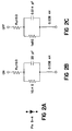
- FIGS. 2b and 2c represent the equivalent circuit models of a typical 2- ⁇ m i-region GaAs p-i-n diode with a cutoff frequency with f c > 2THz for a p-i-n diode of a particular size as illustrated in FIG. 2a.
- the series off capacitance is relatively substantial.
- two p-i-n diodes in series may be utilized in order to extend the bandwidth response at the expense of insertion loss.
- the individual input switch arms 22-36 of the radially combined microstrip switch 20 will have a frequency response beyond the frequency of interest. It is the low pass roll-characteristic of the radially combined microstrip switch which will be the limiting performance factor for an N-way microstrip switch at millimeter-wave frequencies.
- the radially combined patch 40 will be of significant area and will contribute to the dominant low-pass loss characteristics of the N-way switch 20 at millimeter-wave frequencies.
- the radial combined patch 40 By reducing the size of the radial combined patch 40, the associated parasitic impedances can be minimized and the frequency response extended.
- the width of the output 50 ⁇ microstrip transmission line 38 for example 70 ⁇ m for a 4 mil GaAs substrate, will ultimately limit how small the radial combined patch 40 can be made as generally illustrated in FIG. 9.
- FIG. 3 illustrates a lumped element equivalent circuit of the single pole N-throw radial combined microstrip switch 20 illustrated in FIG. 1.
- the radially combined patch 40 can be represented by a L-C low pass network 41.
- the thru-path of the Nth input switch arm 36 can be represented by the equivalent circuit illustrated in FIG. 4.
- the low pass response of the microstrip switch 20 can be characterized by simple low pass filter network formed from a series inductance L feed and the effective parallel combination of the shunt capacitors C off (N-1)/2 and C feed .
- the shunt capacitant C feed can typically account for ⁇ 15% of the total effective shunt capacitance.
- the shunt capacitance C feed is large and the associated series inductance L feed is small. If the electrical and physical restraints allow the reduction of the diameter of the radially combined patch 40, the shunt capacitance of the radially combined patch 40 will become relatively smaller; however, the input microstrip transmission lines 44 will become more inductive.
- the present invention relates to a microstrip switch which includes N-input switch arms and an output port, formed from a microstrip transmission line.
- Each input switch arm includes one or more p-i-n diodes.
- the input switch arms as well as the output port are connected at a radially combined patch.
- the radially combined patch is air suspended in order to reduce the parasitic shunt capacitance in order to extend the low pass frequency response of the switch.
- the present invention relates to a radially combined microstrip switch with on reduced insertion loss characteristic at millimeter wave frequencies.
- the stray shunt capacitances of the switch are reduced by removing the high dielectric material beneath the radial combined center patch in accordance with the present invention.
- the shunt capacitance can be reduced by an order of magnitude.
- FIG. 5a illustrates a planar view of an N-way radially combined single pole N-throw microstrip switch 60 in accordance with the present invention.
- the microstrip switch 60 includes N input switch arms 62, 64, 66, 68, 70, 71, and 72 and a an output arm 74 which defines an output port.
- FIG. 5a illustrates 7 input switch arms 62-72 and a single output port 74, it is clear that the principles of the present invention are applicable to virtually any number of input arms.
- Each of the input switch arms 62-72 includes an input microstrip transmission line 76, for example 50 ⁇ , one or more serially coupled p-i-n diodes 78 and an interconnecting microstrip transmission line 80.
- Each of the interconnecting microstrip transmission lines 80 are radially connected to a patch 84.
- the output arm 74 for example, a 50 ⁇ microstrip transmission line, is also connected to the radially combined patch 84.
- the radially combined patch 84 is air suspended as better illustrated in FIG. 5b.
- the radially combined single pole N-throw microstrip switch 60 in accordance with the present invention may be formed on a suitable type III-V substrate 86, such as a GaAs substrate.
- An important aspect of the invention relates to the cavity 88 under the radially combined patch 84.
- a top side 90 of the substrate 90 is processed by conventional processing techniques to form the top side 90 structure illustrated in FIG. 5B.
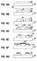
- the wafer maybe flip mounted for fabricating the radial cavity as illustrated in FIG. 6a-6i.
- FIG. 6a-6i illustrate the processing steps for fabricating the cavity 88 in the substrate 86.
- the processing steps are compatible with conventional MMIC processing technology.
- the substrate 86 is mounted frontside down onto a supporting mechanical wafer 92, such as a silicon wafer.
- a photoresist 94 is spun on top of the substrate 86.
- a photomask 96 is used to mask off the region for the cavity 88.
- the photoresist 94 is exposed by way of the mask 96 and developed to expose an area 98 of the substrate 86 which will be removed to form the cavity 88.
- the cavity 88 may be formed by etching, for example, reactive ion etching (RIE), completely through the substrate 86 in order to form the cavity 88.
- RIE reactive ion etching
- a planarizing photoresist 100 such as AZ 9620, to cover the exposed portions of 102 and 104 of the substrate 86 as well as the cavity 88.
- a backside metal 106 is deposited beneath the substrate 86.
- a second mask 108 is used to define the regions for the backside metal 106.
- the planarizing photoresist 102 is exposed by way of the mask 108 and developed to form the structure illustrated in FIG. 6e.
- step 6F the backside metal, for example, Ti-Au, is deposited onto the exposed areas 102 and 104 of the substrate 86 as well as on top of the planarizing photoresist 100.
- the backside metal 106 as well as the metallization 108 covering the cavity 88 is developed by conventional liftoff techniques by developing the planarizing photoresist 100 which removes the metal 108 from the cavity 108 as generally shown in FIG. 6g.
- This metallization forms the backside metal plane of the microstrip transmission media. Vias from the top side to backside ground are formed from the selective metal evaporation process mentioned above.
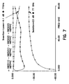
- FIGS. 7 and 8 illustrate the insertion loss, return loss and isolation performance of a single pole 8 throw (SP8T) p-i-n diode microstrip switch fabricated utilizing a conventional construction and a microstrip switch fabricated in accordance with the present invention, respectively.
- SP8T single pole 8 throw
- the conventional microswitch radially combined microstrip switch achieves -9.1 dB insertion loss, 5 dB return loss and 23dB isolation.
- the radially combined microstrip switch, fabricated in accordance with the present invention achieves an air insertion loss of 3.6 dB, 10dB return loss and about 17 dB isolation.
- the microswitch in accordance with the present invention proves the insertion loss by as much as 5.5 dB at 77 GHz.
- FIG. 9 illustrates a typical layout of SP8T radially combined p-i-n diode microswitch illustrating the physical size constraints of the radial topology. As shown, there is limit to how small the area of the radial patch can be laid out due to the physical size constraint of the radial combined patch which is governed by the size and number of switch arms. Also, the electrical performance constrains how small the center combiner can be since the arm isolation and 50 ⁇ output patch will degrade with small combiner patch geometry.
- CMOS Technology Micromachined Coplanar Waveguides in CMOS Technology
- a coplanar waveguide formed from CMOS Technology is formed with a V-shaped cavity beneath a microstrip structure.
- the V-shaped cavity is formed by rather complicated etching process which includes both isotropic etching and anastropic etching.
- the principles of the present invention are adapted to be applied to the coplanar waveguide in order to provide a relatively simplified process for forming the cavity under the microstrip. More particularly, the process in accordance with the present invention described above may be used to fabricate a coplanar wave guide. However, parts of the center majority conductor may be suspended while leaving parts of the substrate for mechanical support. A top and cross-sectional drawing of such a CPW structure is represented in FIG. 6h and 6i.
Landscapes
- Engineering & Computer Science (AREA)
- Manufacturing & Machinery (AREA)
- Waveguide Switches, Polarizers, And Phase Shifters (AREA)
Applications Claiming Priority (2)
| Application Number | Priority Date | Filing Date | Title |
|---|---|---|---|
| US3197 | 1993-01-11 | ||
| US09/003,197 US5986517A (en) | 1998-01-06 | 1998-01-06 | Low-loss air suspended radially combined patch for N-way RF switch |
Publications (3)
| Publication Number | Publication Date |
|---|---|
| EP0929113A2 true EP0929113A2 (fr) | 1999-07-14 |
| EP0929113A3 EP0929113A3 (fr) | 1999-07-28 |
| EP0929113B1 EP0929113B1 (fr) | 2007-02-14 |
Family
ID=21704666
Family Applications (1)
| Application Number | Title | Priority Date | Filing Date |
|---|---|---|---|
| EP98124818A Expired - Lifetime EP0929113B1 (fr) | 1998-01-06 | 1998-12-30 | Plaque d'un combineur radial à faible perte, suspendue dans l'air, pour un commutateur RF à N voies |
Country Status (4)
| Country | Link |
|---|---|
| US (1) | US5986517A (fr) |
| EP (1) | EP0929113B1 (fr) |
| JP (1) | JP3472495B2 (fr) |
| DE (1) | DE69837078T2 (fr) |
Cited By (2)
| Publication number | Priority date | Publication date | Assignee | Title |
|---|---|---|---|---|
| WO2005109636A1 (fr) * | 2004-05-06 | 2005-11-17 | Koninklijke Philips Electronics N.V. | Dispositif electronique |
| CN103018927A (zh) * | 2012-12-24 | 2013-04-03 | 中国计量学院 | 八爪圆环结构的太赫兹波开关 |
Families Citing this family (5)
| Publication number | Priority date | Publication date | Assignee | Title |
|---|---|---|---|---|
| US6465367B1 (en) * | 2001-01-29 | 2002-10-15 | Taiwan Semiconductor Manufacturing Company | Lossless co-planar wave guide in CMOS process |
| US6552371B2 (en) * | 2001-02-16 | 2003-04-22 | Teraburst Networks Inc. | Telecommunications switch array with thyristor addressing |
| US7298228B2 (en) * | 2002-05-15 | 2007-11-20 | Hrl Laboratories, Llc | Single-pole multi-throw switch having low parasitic reactance, and an antenna incorporating the same |
| US20090077871A1 (en) * | 2007-05-04 | 2009-03-26 | Alex Berg Gebert | Process for obtaining low and medium molecular weight Polyphenols and standardized solid fuel from tree wood or bark |
| CN114142190B (zh) * | 2021-11-29 | 2023-04-07 | 中北大学 | 一种王字型上电极式单刀双掷开关 |
Family Cites Families (7)
| Publication number | Priority date | Publication date | Assignee | Title |
|---|---|---|---|---|
| US3223947A (en) * | 1963-09-11 | 1965-12-14 | Motorola Inc | Broadband single pole multi-throw diode switch with filter providing matched path between input and on port |
| BE756728A (fr) * | 1969-10-01 | 1971-03-01 | Western Electric Co | Commutateur a lignes a bandes pour haute frequence |
| FR2239820A1 (en) * | 1973-08-03 | 1975-02-28 | Trt Telecom Radio Electr | Broadband HF commutator with transistor and diode switches - is designed to reduce capacitance of commutated matched lines coupled to common output |
| US4127830A (en) * | 1977-05-26 | 1978-11-28 | Raytheon Company | Microstrip switch wherein diodes are formed in single semiconductor body |
| US4302734A (en) * | 1980-03-12 | 1981-11-24 | Nasa | Microwave switching power divider |
| US4525689A (en) * | 1983-12-05 | 1985-06-25 | Ford Aerospace & Communications Corporation | N×m stripline switch |
| US4673958A (en) | 1985-01-31 | 1987-06-16 | Texas Instruments Incorporated | Monolithic microwave diodes |
-
1998
- 1998-01-06 US US09/003,197 patent/US5986517A/en not_active Expired - Lifetime
- 1998-12-30 EP EP98124818A patent/EP0929113B1/fr not_active Expired - Lifetime
- 1998-12-30 DE DE69837078T patent/DE69837078T2/de not_active Expired - Lifetime
-
1999
- 1999-01-06 JP JP00139699A patent/JP3472495B2/ja not_active Expired - Fee Related
Cited By (4)
| Publication number | Priority date | Publication date | Assignee | Title |
|---|---|---|---|---|
| WO2005109636A1 (fr) * | 2004-05-06 | 2005-11-17 | Koninklijke Philips Electronics N.V. | Dispositif electronique |
| US8901703B2 (en) | 2004-05-06 | 2014-12-02 | Nxp, B.V. | Electronic device |
| CN103018927A (zh) * | 2012-12-24 | 2013-04-03 | 中国计量学院 | 八爪圆环结构的太赫兹波开关 |
| CN103018927B (zh) * | 2012-12-24 | 2014-12-10 | 中国计量学院 | 八爪圆环结构的太赫兹波开关 |
Also Published As
| Publication number | Publication date |
|---|---|
| EP0929113B1 (fr) | 2007-02-14 |
| JPH11251802A (ja) | 1999-09-17 |
| US5986517A (en) | 1999-11-16 |
| JP3472495B2 (ja) | 2003-12-02 |
| DE69837078D1 (de) | 2007-03-29 |
| EP0929113A3 (fr) | 1999-07-28 |
| DE69837078T2 (de) | 2007-06-06 |
Similar Documents
| Publication | Publication Date | Title |
|---|---|---|
| US6043727A (en) | Reconfigurable millimeterwave filter using stubs and stub extensions selectively coupled using voltage actuated micro-electro-mechanical switches | |
| Yang et al. | A novel low-loss slow-wave microstrip structure | |
| US20030128084A1 (en) | Compact bandpass filter for double conversion tuner | |
| Dey et al. | RF MEMS switches, switching networks and phase shifters for microwave to millimeter wave applications | |
| US5986517A (en) | Low-loss air suspended radially combined patch for N-way RF switch | |
| US8081050B2 (en) | Multilayer planar tunable filter | |
| Chaturvedi et al. | Millimeter-wave passive bandpass filters | |
| US7274278B2 (en) | Tunable micro electromechanical inductor | |
| Rebeiz et al. | Micromachined membrane filters for microwave and millimeter‐wave applications (invited article) | |
| EP0411919A2 (fr) | Circuit d'adaptation de transistor à haute fréquence | |
| US7382215B1 (en) | Image guide coupler switch | |
| JP3564937B2 (ja) | 超電導薄膜回路 | |
| US20220131275A1 (en) | Apparatus for waveguide transition and antenna array having the same | |
| Zhu et al. | Micromachined silicon via-holes and interdigital bandpass filters | |
| Kwon et al. | RF MEMS--Enabling Technology for Millimeter-Waves | |
| JP2000151223A (ja) | 半導体装置 | |
| KR100753638B1 (ko) | 마이크로기계가공 기술을 이용한 CPW―fedpost―supported 패치 안테나 및 그 제조방법 | |
| CN220963708U (zh) | 一种硅基GaN宽阻带高选择性毫米波在片滤波器 | |
| Drozdovski | SPST switches for satellite communications systems | |
| Sharma et al. | Parametric analysis of w-band rf mems spdt switch | |
| Hettak et al. | Simultaneous realization of millimeter wave uniplanar shunt stubs and DC block | |
| CN116885413A (zh) | 一种螺旋缺陷结构的在片交指带通滤波器及其制备方法 | |
| Srinivasa Rao et al. | Design and performance analysis of hybrid SPDT RF MEMS switch | |
| KR100199019B1 (ko) | 마이크로파용 듀플렉서 및 그 제조방법 | |
| CN117525782A (zh) | 硅基氮化镓宽阻带高选择性片上带通滤波器及其制备方法 |
Legal Events
| Date | Code | Title | Description |
|---|---|---|---|
| PUAI | Public reference made under article 153(3) epc to a published international application that has entered the european phase |
Free format text: ORIGINAL CODE: 0009012 |
|
| PUAL | Search report despatched |
Free format text: ORIGINAL CODE: 0009013 |
|
| AK | Designated contracting states |
Kind code of ref document: A2 Designated state(s): DE FR GB |
|
| AX | Request for extension of the european patent |
Free format text: AL;LT;LV;MK;RO;SI |
|
| RIC1 | Information provided on ipc code assigned before grant |
Free format text: 6H 01P 1/15 A, 6H 01P 11/00 B |
|
| AK | Designated contracting states |
Kind code of ref document: A3 Designated state(s): AT BE CH CY DE DK ES FI FR GB GR IE IT LI LU MC NL PT SE |
|
| AX | Request for extension of the european patent |
Free format text: AL;LT;LV;MK;RO;SI |
|
| 17P | Request for examination filed |
Effective date: 19990907 |
|
| AKX | Designation fees paid |
Free format text: DE FR GB |
|
| 17Q | First examination report despatched |
Effective date: 20030801 |
|
| RAP1 | Party data changed (applicant data changed or rights of an application transferred) |
Owner name: NORTHROP GRUMMAN CORPORATION |
|
| RAP1 | Party data changed (applicant data changed or rights of an application transferred) |
Owner name: NORTHROP GRUMMAN CORPORATION |
|
| GRAP | Despatch of communication of intention to grant a patent |
Free format text: ORIGINAL CODE: EPIDOSNIGR1 |
|
| GRAS | Grant fee paid |
Free format text: ORIGINAL CODE: EPIDOSNIGR3 |
|
| GRAA | (expected) grant |
Free format text: ORIGINAL CODE: 0009210 |
|
| AK | Designated contracting states |
Kind code of ref document: B1 Designated state(s): DE FR GB |
|
| REG | Reference to a national code |
Ref country code: GB Ref legal event code: FG4D |
|
| REF | Corresponds to: |
Ref document number: 69837078 Country of ref document: DE Date of ref document: 20070329 Kind code of ref document: P |
|
| ET | Fr: translation filed | ||
| PLBE | No opposition filed within time limit |
Free format text: ORIGINAL CODE: 0009261 |
|
| STAA | Information on the status of an ep patent application or granted ep patent |
Free format text: STATUS: NO OPPOSITION FILED WITHIN TIME LIMIT |
|
| 26N | No opposition filed |
Effective date: 20071115 |
|
| PGFP | Annual fee paid to national office [announced via postgrant information from national office to epo] |
Ref country code: GB Payment date: 20071227 Year of fee payment: 10 |
|
| PGFP | Annual fee paid to national office [announced via postgrant information from national office to epo] |
Ref country code: FR Payment date: 20071217 Year of fee payment: 10 |
|
| GBPC | Gb: european patent ceased through non-payment of renewal fee |
Effective date: 20081230 |
|
| REG | Reference to a national code |
Ref country code: FR Ref legal event code: ST Effective date: 20090831 |
|
| PG25 | Lapsed in a contracting state [announced via postgrant information from national office to epo] |
Ref country code: GB Free format text: LAPSE BECAUSE OF NON-PAYMENT OF DUE FEES Effective date: 20081230 |
|
| PG25 | Lapsed in a contracting state [announced via postgrant information from national office to epo] |
Ref country code: FR Free format text: LAPSE BECAUSE OF NON-PAYMENT OF DUE FEES Effective date: 20081231 |
|
| PGFP | Annual fee paid to national office [announced via postgrant information from national office to epo] |
Ref country code: DE Payment date: 20101222 Year of fee payment: 13 |
|
| REG | Reference to a national code |
Ref country code: DE Ref legal event code: R082 Ref document number: 69837078 Country of ref document: DE Representative=s name: WUESTHOFF & WUESTHOFF PATENT- UND RECHTSANWAEL, DE |
|
| REG | Reference to a national code |
Ref country code: DE Ref legal event code: R082 Ref document number: 69837078 Country of ref document: DE Representative=s name: WUESTHOFF & WUESTHOFF, PATENTANWAELTE PARTG MB, DE Effective date: 20120814 Ref country code: DE Ref legal event code: R082 Ref document number: 69837078 Country of ref document: DE Representative=s name: WUESTHOFF & WUESTHOFF PATENT- UND RECHTSANWAEL, DE Effective date: 20120814 Ref country code: DE Ref legal event code: R081 Ref document number: 69837078 Country of ref document: DE Owner name: NORTHROP GRUMMAN SYSTEMS CORPORATION, LOS ANGE, US Free format text: FORMER OWNER: NORTHROP GRUMMAN CORP., LOS ANGELES, CALIF., US Effective date: 20120814 Ref country code: DE Ref legal event code: R081 Ref document number: 69837078 Country of ref document: DE Owner name: NORTHROP GRUMMAN SYSTEMS CORPORATION, US Free format text: FORMER OWNER: NORTHROP GRUMMAN CORP., LOS ANGELES, US Effective date: 20120814 |
|
| REG | Reference to a national code |
Ref country code: DE Ref legal event code: R119 Ref document number: 69837078 Country of ref document: DE Effective date: 20120703 |
|
| PG25 | Lapsed in a contracting state [announced via postgrant information from national office to epo] |
Ref country code: DE Free format text: LAPSE BECAUSE OF NON-PAYMENT OF DUE FEES Effective date: 20120703 |