EP0930574A2 - Processeur parallèle et méthode de traitement - Google Patents
Processeur parallèle et méthode de traitement Download PDFInfo
- Publication number
- EP0930574A2 EP0930574A2 EP99400094A EP99400094A EP0930574A2 EP 0930574 A2 EP0930574 A2 EP 0930574A2 EP 99400094 A EP99400094 A EP 99400094A EP 99400094 A EP99400094 A EP 99400094A EP 0930574 A2 EP0930574 A2 EP 0930574A2
- Authority
- EP
- European Patent Office
- Prior art keywords
- sub
- page
- bus
- memory
- access request
- Prior art date
- Legal status (The legal status is an assumption and is not a legal conclusion. Google has not performed a legal analysis and makes no representation as to the accuracy of the status listed.)
- Withdrawn
Links
Images




Classifications
-
- G—PHYSICS
- G06—COMPUTING OR CALCULATING; COUNTING
- G06F—ELECTRIC DIGITAL DATA PROCESSING
- G06F15/00—Digital computers in general; Data processing equipment in general
- G06F15/16—Combinations of two or more digital computers each having at least an arithmetic unit, a program unit and a register, e.g. for a simultaneous processing of several programs
-
- G—PHYSICS
- G06—COMPUTING OR CALCULATING; COUNTING
- G06F—ELECTRIC DIGITAL DATA PROCESSING
- G06F12/00—Accessing, addressing or allocating within memory systems or architectures
- G06F12/02—Addressing or allocation; Relocation
- G06F12/08—Addressing or allocation; Relocation in hierarchically structured memory systems, e.g. virtual memory systems
-
- G—PHYSICS
- G06—COMPUTING OR CALCULATING; COUNTING
- G06F—ELECTRIC DIGITAL DATA PROCESSING
- G06F12/00—Accessing, addressing or allocating within memory systems or architectures
- G06F12/02—Addressing or allocation; Relocation
- G06F12/08—Addressing or allocation; Relocation in hierarchically structured memory systems, e.g. virtual memory systems
- G06F12/0802—Addressing of a memory level in which the access to the desired data or data block requires associative addressing means, e.g. caches
- G06F12/0806—Multiuser, multiprocessor or multiprocessing cache systems
- G06F12/0811—Multiuser, multiprocessor or multiprocessing cache systems with multilevel cache hierarchies
-
- G—PHYSICS
- G06—COMPUTING OR CALCULATING; COUNTING
- G06F—ELECTRIC DIGITAL DATA PROCESSING
- G06F2212/00—Indexing scheme relating to accessing, addressing or allocation within memory systems or architectures
- G06F2212/25—Using a specific main memory architecture
- G06F2212/251—Local memory within processor subsystem
-
- G—PHYSICS
- G06—COMPUTING OR CALCULATING; COUNTING
- G06F—ELECTRIC DIGITAL DATA PROCESSING
- G06F2212/00—Indexing scheme relating to accessing, addressing or allocation within memory systems or architectures
- G06F2212/25—Using a specific main memory architecture
- G06F2212/253—Centralized memory
Definitions
- the present invention relates to a parallel processor comprising a plurality of processor elements and a shared memory connected via a common bus and to a processing method carried out thereon.
- a variety of architectures are being proposed for such parallel processors. Among them, there is one in which a plurality of processor elements and a shared memory are connected to a set of common buses.
- Figure 9 is a view of the system configuration of a general parallel processor 1.
- the parallel processor 1 has built into one chip a common bus 2, n number of processor elements 3 1 to 3 n , a shared memory 4, and a bus unit 5.
- the common bus 2 has connected to it the processor elements 3 1 to 3 n , the shared memory 4, and the bus unit 5.
- the bus unit 5 is connected to a main memory 7 via an external chip interface 6.
- One data port I/O is provided in a memory cell region 4a of the shared memory 4.
- data is transferred via the common bus 2 and the data port I/O when the processor elements 3 1 to 3 n access the data stored in the shared memory 4.
- An object of the present invention is to provide a parallel processor and a processing method which can exhibit a high processing performance.
- a parallel processor of the present invention comprises a plurality of processor elements, each including an internal memory storing one or more sub-pages and performing processing using data stored in the internal memory; a first bus connected to the plurality of processor elements; a second bus connected to an external memory; and a shared memory connected to both the first and second buses, the shared memory including a storage means having a plurality of sub-banks storing the sub-pages, a control means for controlling data transfer between the internal memory of the processor element and the storage means through the first bus and data transfer between the storage means and the external memory through the second bus, and an access request management means for receiving as input an access request which generates a page fault to the storage means from the processor elements, storing another access request when another access request is input during the data transfer due to the access request between the shared memory and the external memory through the second bus, and causing the control means to execute the stored other access request when the stored other access request does not generate a page fault.
- the access request management means enables storage of a plurality of access requests and makes the control means execute an access request among the plurality of stored access requests which does not generate a page fault when a plurality of access requests are stored prior to a stored access request generating a page fault.
- the processing method of the present invention comprises storing one or more sub-pages in a shared memory having a storage region comprising a plurality of sub-banks each having a single data port and accessed by a plurality of processor elements; controlling data transfer between an internal memory of a processor element and the shared memory through a first bus and data transfer between the shared memory and an external memory through a second bus in response to an access request from the processor element; and, when a processor element issues an access request accompanied with a page fault to the shared memory and during the transfer of data between the shared memory and external memory through the second bus in response to that access request another processor element issues an access request, storing the access request issued by the other processor element, judging if the stored access request causes a page fault or not, and, when judging that it does not cause a page fault, executing the stored access request.
- Figure 1 is a view of the system configuration of a parallel processor 21 of the present embodiment.
- the parallel processor 21 comprises, for example, a common bus 22 as a first bus, processor elements 23 1 to 23 n , a shared memory 24, a bus unit 25, and an external access bus 26 as a second bus.
- the processor elements 23 1 to 23 n and the shared memory 24 are connected to the common bus 22. Also, the shared memory 24 and the bus unit 25 are connected to the external access bus 26.
- the common bus 22 has a bus width of 128 bits, while the external access bus 26 has a bus width of 32 bits.
- the common bus 22 has a data transfer rate of more than four times that of the external access bus 26.
- each of the processor elements 23 1 to 23 n has a program counter and carries out the processing independently from the others in response to instructions stored at addresses of an instruction memory, not illustrated, indicated by the program counter.
- processor elements 23 1 to 23 n for example, RISC (reduced instruction set computer) type general-purpose processors may be used.
- the processor elements 23 1 to 23 n are provided with sub-banks 27 1 , 27 2 , and 27 3 as internal memories which can store a plurality of sub-pages, for example, three sub-pages.
- a sub-page is 521 bytes of data stored in storage regions of continuous addresses on a main memory 7, and one page is composed by sub-pages of four continuous addresses.
- the processor elements 23 1 to 23 n read the sub-pages from the shared memory 24 and store the same in the sub-banks 27 1 to 27 3 , but it is possible to store sub-pages of different pages among the processor elements 23 1 to 23 n and among the sub-banks 27 1 to 27 3 .
- the bus unit 25 is connected to the main memory 7 via a chip interface 6 provided outside the parallel processor 21.
- the main memory 7 has a memory space having 4 Gbytes of continuous addresses.
- Figure 2 is a view of the configuration of the shared memory 24 shown in Fig. 1.
- the shared memory 24 comprises, for example, a common bus control circuit 31, an external bus control circuit 32, a control circuit 33, memory internal buses 51 and 52, multiplexers (MUX) 53, 54, 55, and 56, a memory cell region 90 as a first memory means, address decoders 57, 58, 59, and 60, a tag data region 120 as a second memory means, and a request queue 125.
- a common bus control circuit 31 an external bus control circuit 32
- a control circuit 33 memory internal buses 51 and 52
- multiplexers (MUX) 53, 54, 55, and 56 multiplexers 53, 54, 55, and 56
- a memory cell region 90 as a first memory means
- address decoders 57, 58, 59, and 60 address decoders 57, 58, 59, and 60
- tag data region 120 as a second memory means
- a request queue 125 a request queue 125.
- the common bus control circuit 31, the external bus control circuit 32, and the control circuit 33 function as a control means.
- the control circuit 33 controls the common bus control circuit 31, the external bus control circuit 32, the multiplexers 53 to 56, and the address decoders 57 to 60.
- the control circuit 33 judges whether or not the requested sub-page is stored in the memory cell region 90 or not (whether a page hit exists or not) by referring to tag data as characteristic data stored in the tag data region 120.
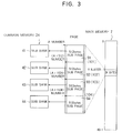
- the control circuit determines the page to be covered by the replacement with the page to be exchanged with from the main memory 7 from among a plurality of pages stored in the main memory cell region 90 by a method explained later with reference to Fig. 3.
- control circuit 33 controls the page transfer between the shared memory 24 and the main memory 7 so as to transfer the sub-pages requested by the processor elements 23 1 to 23 n first from the main memory 7 to the shared memory 24.
- the common bus control circuit 31 controls the transfer of the sub-pages between the processor elements 23 1 to 23 n and the memory sub-banks 41 to 44 via the memory internal bus 51 and the common bus 22. Specifically, the common bus control circuit 31 controls the address decoders 57 to 60 by outputting a control signal S31 and controls the switching of the multiplexers 53 and 54 based on a control signal from the control circuit 33.
- the external bus control circuit 32 controls the page transfer between the memory sub-banks 41 to 44 and the main memory 7 via the memory internal bus 52 and the external access bus 26. Specifically, the external bus control circuit 32 outputs a control signal S32 to control the address decoders 57 to 60 and controls the switching of the multiplexers 53 and 54 based on the control signal from the control circuit 33.
- the multiplexers 53 to 56 connect the respective memory sub-banks 41 to 44 to one of the memory internal bus 51 or 52 based on the control signals S31 and S32 and a control signal from the control circuit 33.
- the address decoders 57 to 60 decode the control signals S31 and S32 to control the access to the memory sub-banks 41 to 44.
- the memory cell region 90 is physically and equally divided into four memory sub-banks 41 to 44. Each of the memory sub-banks 41 to 44 is provided with a single data port.
- the memory cell region 90 is divided by m number of banks 80 n to 80 m-1 in order to be equally distributed among the memory sub-banks 41 to 44.
- Each of the memory sub-banks 41 to 44 has a memory capacity able to store, for example, m number of sub-pages. Note that the sub-pages include image data.
- the memory sub-banks 41 to 44 exchange data in sub-page units among the processor elements 23 1 to 23 n via the multiplexers 53 to 56, the memory internal bus 51, and the common bus 22.
- the "exchanging of data” includes a write operation of data from the processor elements 23 1 to 23 n to the memory sub-banks 41 to 44, a read operation of data from the processor elements 23 1 to 23 n to the memory sub-banks 41 to 44, and both of the operations.
- the memory banks 41 to 44 exchange data with the main memory 7 in page units stored in the banks 80 0 to 80 m-1 via the multiplexers 53 to 56, the memory internal bus 52, and the external access bus 26.
- one page is 2 Kbytes and is composed of 4 sub-pages.
- the head address of the sub-pages which the processor elements 23 1 to 23 n are trying to access is the address A, address (A+512), address (A+1024), or address (A+1536)
- address A address (A+512), address (A+1024), or address (A+1536)
- one page's worth of data stored in 2 Kbytes of continuous addresses from the address A in the main memory 7 is transferred to the shared memory 4, then the one page's worth of data is divided into four sub-pages and is stored in the banks 80 n to 80 m .
- a 4 Gbyte memory space of the main memory 7 is indicated by a 32-bit address.
- the 31st to 11th bits of the 32-bit address indicate the head address of the page and the 10th to 0th bits indicate the address within the page.
- the 10th and 9th bits indicate a sub-bank.
- the amount of the data of the sub-pages stored in the memory sub-banks 41 to 44 be standardized in the system as a whole so that the sub-pages can be used in common by all of the processor elements 23 1 to 23 n .
- the memory capacity of the sub-bank 27 1 of the processor elements 23 1 to 23 n is set to 512 bytes and the amount of data of a sub-page is also set to 512 bytes.
- the tag data region 120 stores, as shown in Fig. 2, tag data as the characteristic data of a sub-page stored in the memory cell region 90 composed of the memory sub-banks 41 to 44.
- the tag data region 120 has tag banks 130 0 to 130 m-1 which correspond to the banks 80 n to 80 m-1 .
- Data indicating the characteristics of the sub-pages stored in the respective banks 80 n to 80 m are stored in the tag banks 130 0 to 130 m-1 .
- the tag data is comprised of a valid identification region 121, a dirty identification region 122, and a page selector region 123.
- the valid identification region 121 is provided with one valid bit indicating the validity of the data of a sub-page for each of the sub-pages. For example, “1" indicating “valid” is set for the valid bit corresponding to a valid sub-page in the valid identification region 121, while “0” indicating “invalid” is set for the valid bit corresponding to an invalid sub-page.
- the dirty identification region 122 is provided with one dirty bit indicating whether data of a sub-page is dirty or not for each sub-page.
- dirty means that there was a write operation from the processor elements 23 1 to 23 n to the sub-page in question.
- the sub-page has to be written back in the main memory 7. Namely, a write back operation is necessary.
- the page selector region 123 has a page selector indicating an identification number of a page (for example, the head address of a page) stored in the banks 80 n to 80 m .
- the request queue 125 stores the access requests in a queue and outputs the same to the control circuit 33 in the procedure shown below for execution.
- Figure 4 is a view of the configuration of the request queue 125.
- the request queue 125 has a queue entry block 300, a control circuit 310. and a multiplexer 312.
- the queue entry block 300 is configured by six queue entry banks 301 to 306 connected in order.
- the queue entry bank 301 is connected to the memory internal bus 51 and inputs and stores access requests such as a sub-page exchange request signal to the memory cell region 90 from the processor elements 23 1 to 23 n via the common bus 22 and memory internal bus 51.
- the queue entry bank 301 outputs the stored access requests to the queue entry bank 301 or multiplexer 312 of the following stage in response to control from the control circuit 310.
- the queue entry banks 302 to 305 in response to control from the control circuit 310, input and store the access requests from the queue entry banks 301 to 304 of the previous stage and output the stored access requests to the queue entry banks 303 to 306 or the multiplexer 312 of the following stage.
- the queue entry bank 306 in response to control from the control circuit 310, inputs and stores the access requests from the queue entry bank 305 and outputs the stored access requests in question to the multiplexer 312.
- the multiplexer 312 in response to the control from the control circuit 310, is connected to one of the queue entry banks 301 to 306 to the control circuit 33 and output the access requests stored in the connected queue entry bank to the control circuit 33.
- Figure 5 is a view for explaining an operation of the request queue 125 in the case of no preemptive reading of access requests.
- access requests R j+0 , R j+1 , R j+2 , R j+3 , R j+4 , and R j+5 are generated from the processor elements 23 2 to 23 n .
- all of the access requests R j+0 to R j+5 are, for example, accesses not accompanied with page faults.
- the access requests R j+0 , R j+1 , R j+2 , R j+3 , R j+4 , and R j+5 are respectively stored in the queue entry banks 306, 305, 304, 303, 302, and 301.
- the queue entry bank 306 and the control circuit 33 are connected via the multiplexer 312 by the control from the control circuit 310 shown in Fig. 4 and the access request R j+0 stored in the queue entry bank 306 is output to the control circuit 33.
- access processing to the memory cell region 90 in response to the access request R j+0 starts.
- the access requests R j+1 , R j+2 , R j+3 , R j+4 , and R j+5 are shifted (transferred) and stored in the respective queue entry banks 306, 305, 304, 303, and 302. Also, the access request R j+6 from the processor elements 23 1 to 23 n are stored in the queue entry bank 301 via the common bus 22 and memory internal bus 51. As a result, the state of storage of the queue entry block 300 becomes as shown in Fig. 5B.
- Figure 6 is a view for explaining the operation of the request queue 125 in the case of preemptive reading of access requests.
- the access requests R j+0 , R j+1 , R j+2 , R j+3 , R j+4 , and R j+5 are stored in the queue entry banks 306, 305, 304, 303, 302, and 301 as shown in Fig. 6A.
- an access having a page fault arises in the sub-page 351 by the access request R j-1 , and a page composed of sub-pages 350 to 353 is transferred from the main memory 7 shown in Fig. 1 to the bank 80 6 of the memory cell region 90 shown in Fig. 7 via the external access bus 26.
- control circuit 310 shown in Fig. 4 determines whether or not the respectively stored access requests are ready to be executed from the queue entry banks 301 toward 306 in order.
- the control circuit 310 judges, for example, that the access request R j+0 and R j+1 have page faults and are not ready to be executed, while because the access request R j+2 is an access without page fault and an access to the sub-page 362 stored in the different bank 80 9 which is different from the bank 80 6 , judges that the access request R j+2 is ready to be executed.
- the queue entry bank 304 and the control circuit 310 are connected via the multiplexer 312, and the access request R j+2 stored in the queue entry bank 304 is output to the control circuit 33. Due to this, the access request R j+2 is executed and the sub-page 362 is output to the processor elements 23 1 to 23 n which made the access request R j+2 via the common bus 22. Namely, the access request R j+2 is executed prior to the access requests R j+0 and R j+1 .
- page transfer processing between the main memory 7 and the shared memory 24 via the external access bus 26 by the access request R j-1 and the sub-page transfer processing between the shared memory 24 and the processor elements 23 1 to 23 n via the common bus 22 by the access request R j+2 are performed in parallel.
- the access requests R j+3 , R j+4 , and R j+5 are shifted (transferred) and stored respectively in the queue entry banks 304, 302, and 302.
- the access request R j+6 from the processor elements 23 1 to 23 n is stored in the queue entry bank 301 via the common bus 22 and the memory internal bus 51.
- the access requests R j+0 and R j+1 are respectively stored in the queue entry banks 306 and 305 continuously. Due to this, the state of storage of the queue entry block 300 becomes as shown in Fig. 6B.
- a control signal S31 is output from the common bus control circuit 31 to the address decoder 58 and the multiplexer 54 is connected to the memory internal bus 51.
- the sub-page 112 is output to the processor element 23 4 via the memory internal bus 51 and the common bus 22.
- exchange processing of the sub-pages 91 to 94 stored in the bank 80 1 of the shared memory 24 and the sub-pages 101 to 104 stored in the main memory 7 is carried out in parallel to the transfer processing of the sub-page 112.
- the exchange processing of sub-pages between the processor elements 23 1 to 23 n and the shared memory 24 and the exchange processing of pages between the shared memory 24 and the main memory 7 can be multiplexly performed.
- the parallel processor 21 it is possible to execute the access requests which are ready to be executed prior to access requests which are output before them without following the output order of the access requests output from the processor elements 23 1 to 23 n to the shared memory 24. Therefore, it is possible to carry out the processing effectively in response to the access requests, and the processing performance can be improved.
- the data within an identical page is continuously accessed from the processor elements 23 1 to 23 n in many cases.
- the parallel processor 21 when a page fault occurs, in addition to a requested sub-page, three other sub-pages having continuous addresses with the requested sub-page are read from the main memory 7 to the shared memory 24, so that the probability that a page fault will occur next can be reduced. Namely, considering the characteristics of image processing, there is a high probability in the near future that access will be made from the processor elements 23 1 to 23 n to a sub-page having a continuous address with the requested sub-page. Thus, reading these sub-pages together with the requested sub-page from the main memory 7 to the shared memory 24 is effective in reducing the rate of occurrence of future page faults.
- sub-page exchange processing between the processor elements 23 1 to 23 n and the shared memory 24 and page exchange processing between the shared memory 24 and the main memory 7 can be performed in parallel by using a memory cell having a one-port structure as memory cells for the shared memory 24, so it is possible to realize high speed processing by a small-sized circuit.
- the shared memory 24 has a single-port structure, but can realize almost the same functional performance as a 2-port structured memory.
- the request queue 125 for storing the access requests by the queue method was given as an example of the access request managing means, however, other than the queue method, the access request managing means can be, for example, configured to receive as input the access requests, stores them at fixed addresses in a predetermined pattern, and output the same to the control circuit 33.
- the request queue 125 is configured by six stages of queue entry banks connected in series was given as an example, however, any number of the queue entry banks may be connected in series. Note that the larger the number, the higher the probability that an access request not accompanied by a page hit will be stored in the request queue 125, therefore the performance of the parallel processor 21 is improved.
- the example was given for a case where the memory cell region of the shared memory 24 is divided into four memory sub-banks 41 to 44, however, any number of memory sub-banks is possible. Accordingly, for example, the memory cell region of the shared memory 24 can be divided into eight memory sub-banks. In this case, one page is composed of eight sub-pages.
- the amount of data of a single sub-page was set to 512 bytes, however, the amount of data is not especially limited and can be 256 bytes, 1024 bytes, etc.
- the sub-pages 91, 93, and 94 stored in the sub-banks 41, 43, and 44 can be exchanged with the main memory 7 in any order after performing the exchange processing of the sub-page 92 stored in the sub-bank 42.
- the exchange was carried out from the requested sub-page 92 to the direction the next address is incremented to, that is, in an order of the sub-pages 93, 94, and 91.
- the exchange can be carried out in an order of the sub-pages 91, 94, and 93 after the sub-page 92, which is the direction of decrementing the addresses.
- a determination circuit may be provided which, for example, determines an operation mode of the processor elements 23 1 and 23 n and determines whether a data access pattern of each processor elements 23 1 to 23 n is in a direction of increasing the main address or decreasing it. In this case, it can be configured to shorten the time for waiting for an access based on the results of determination of the determination circuit by flexibly setting the order of the exchange of sub-pages between the shared memory 24 and the main memory 7.
- a programmable circuit in addition to a fixed logical circuit, such as a sequencer capable of flexibly changing an order of exchange in accordance with conditions as means for controlling the order of exchange of the sub-pages in the shared memory 24.
- the example was given for a case of using one set of the memory internal bus 51 and the common bus 22 as shown in Fig. 2, however a plurality of sets of the memory internal bus 51 and the common bus 22 within the number of the memory sub-banks may be provided. In this case, in accordance with the number of sets, simultaneous accesses become possible from the processor elements 23 1 to 23 n to different banks in the shared memory 24, therefore further higher speed processing can be realized.
- the waiting times of processor elements for accessing a shared memory can be shortened, so a higher processing performance can be realized.
- the waiting times of processor elements for accessing a shared memory can be shortened, so the processor elements can realise higher processing performance.
Landscapes
- Engineering & Computer Science (AREA)
- Theoretical Computer Science (AREA)
- Physics & Mathematics (AREA)
- General Engineering & Computer Science (AREA)
- General Physics & Mathematics (AREA)
- Computer Hardware Design (AREA)
- Software Systems (AREA)
- Memory System Of A Hierarchy Structure (AREA)
- Bus Control (AREA)
- Memory System (AREA)
Applications Claiming Priority (2)
| Application Number | Priority Date | Filing Date | Title |
|---|---|---|---|
| JP10007000A JPH11203192A (ja) | 1998-01-16 | 1998-01-16 | 並列プロセッサおよび演算処理方法 |
| JP700098 | 1998-01-16 |
Publications (1)
| Publication Number | Publication Date |
|---|---|
| EP0930574A2 true EP0930574A2 (fr) | 1999-07-21 |
Family
ID=11653839
Family Applications (1)
| Application Number | Title | Priority Date | Filing Date |
|---|---|---|---|
| EP99400094A Withdrawn EP0930574A2 (fr) | 1998-01-16 | 1999-01-15 | Processeur parallèle et méthode de traitement |
Country Status (4)
| Country | Link |
|---|---|
| US (1) | US6381686B1 (fr) |
| EP (1) | EP0930574A2 (fr) |
| JP (1) | JPH11203192A (fr) |
| KR (1) | KR19990067880A (fr) |
Cited By (7)
| Publication number | Priority date | Publication date | Assignee | Title |
|---|---|---|---|---|
| EP1182559A1 (fr) | 2000-08-21 | 2002-02-27 | Texas Instruments Incorporated | Microprocesseur |
| US6581089B1 (en) * | 1998-04-16 | 2003-06-17 | Sony Corporation | Parallel processing apparatus and method of the same |
| KR100895298B1 (ko) | 2007-04-30 | 2009-05-07 | 한국전자통신연구원 | 멀티미디어 데이터의 효율적인 병렬 처리를 위한 장치,방법, 데이터 처리 엘리먼트 |
| GB2520603B (en) * | 2013-09-26 | 2016-04-06 | Imagination Tech Ltd | Atomic memory update unit and methods |
| US9342478B2 (en) | 2009-02-13 | 2016-05-17 | Samsung Electronics Co., Ltd. | Processor with reconfigurable architecture including a token network simulating processing of processing elements |
| US9466091B2 (en) | 2013-09-26 | 2016-10-11 | Imagination Technologies Limited | Atomic memory update unit and methods |
| US11257271B2 (en) | 2013-09-26 | 2022-02-22 | Imagination Technologies Limited | Atomic memory update unit and methods |
Families Citing this family (16)
| Publication number | Priority date | Publication date | Assignee | Title |
|---|---|---|---|---|
| JP2002024084A (ja) * | 2000-07-12 | 2002-01-25 | Mitsubishi Electric Corp | 半導体集積回路装置および電子システム |
| US6944863B1 (en) * | 2000-12-21 | 2005-09-13 | Unisys Corporation | Queue bank repository and method for sharing limited queue banks in memory |
| US7107386B1 (en) * | 2001-08-08 | 2006-09-12 | Pasternak Solutions, Llc | Memory bus arbitration using memory bank readiness |
| DE10360998B4 (de) * | 2003-12-23 | 2008-09-04 | Infineon Technologies Ag | Schutz von Chips gegen Attacken |
| JP5079988B2 (ja) * | 2005-06-13 | 2012-11-21 | オリンパス株式会社 | 分散処理システム、分散処理方法及びプログラム |
| JP4075914B2 (ja) * | 2005-06-30 | 2008-04-16 | ブラザー工業株式会社 | データ処理装置 |
| KR100748191B1 (ko) * | 2006-04-06 | 2007-08-09 | 엠텍비젼 주식회사 | 공유 메모리를 구비한 장치 및 공유 메모리 억세스 상태정보 제공 방법 |
| US20080189473A1 (en) * | 2007-02-07 | 2008-08-07 | Micron Technology, Inc | Mlc selected multi-program for system management |
| KR101520027B1 (ko) | 2007-06-21 | 2015-05-14 | 삼성전자주식회사 | 움직임 추정 방법 및 장치 |
| US8943296B2 (en) | 2011-04-28 | 2015-01-27 | Vmware, Inc. | Virtual address mapping using rule based aliasing to achieve fine grained page translation |
| US9767039B2 (en) * | 2011-07-18 | 2017-09-19 | Vmware, Inc. | Increasing granularity of dirty bit information in hardware assisted memory management systems |
| US10872393B2 (en) * | 2017-05-15 | 2020-12-22 | Google Llc | Image processor with high throughput internal communication protocol |
| US20230283618A1 (en) * | 2022-03-01 | 2023-09-07 | Western Digital Technologies, Inc. | Detection of malicious operations for distributed cache |
| US12452189B2 (en) | 2022-06-01 | 2025-10-21 | Western Digital Technologies, Inc. | Context-aware NVMe processing in virtualized environments |
| US12386648B2 (en) | 2022-06-09 | 2025-08-12 | Western Digital Technologies, Inc. | Resource allocation in virtualized environments |
| US12379951B2 (en) | 2022-06-27 | 2025-08-05 | Western Digital Technologies, Inc. | Memory coherence in virtualized environments |
Family Cites Families (4)
| Publication number | Priority date | Publication date | Assignee | Title |
|---|---|---|---|---|
| US4843542A (en) * | 1986-11-12 | 1989-06-27 | Xerox Corporation | Virtual memory cache for use in multi-processing systems |
| JP3144794B2 (ja) * | 1990-11-09 | 2001-03-12 | 株式会社日立製作所 | マルチプロセッサシステム |
| US5845329A (en) * | 1993-01-29 | 1998-12-01 | Sanyo Electric Co., Ltd. | Parallel computer |
| US5511224A (en) * | 1993-02-18 | 1996-04-23 | Unisys Corporation | Configurable network using dual system busses with common protocol compatible for store-through and non-store-through cache memories |
-
1998
- 1998-01-16 JP JP10007000A patent/JPH11203192A/ja active Pending
-
1999
- 1999-01-12 US US09/228,653 patent/US6381686B1/en not_active Expired - Fee Related
- 1999-01-13 KR KR1019990000676A patent/KR19990067880A/ko not_active Abandoned
- 1999-01-15 EP EP99400094A patent/EP0930574A2/fr not_active Withdrawn
Cited By (11)
| Publication number | Priority date | Publication date | Assignee | Title |
|---|---|---|---|---|
| US6581089B1 (en) * | 1998-04-16 | 2003-06-17 | Sony Corporation | Parallel processing apparatus and method of the same |
| EP1182559A1 (fr) | 2000-08-21 | 2002-02-27 | Texas Instruments Incorporated | Microprocesseur |
| US6751706B2 (en) | 2000-08-21 | 2004-06-15 | Texas Instruments Incorporated | Multiple microprocessors with a shared cache |
| KR100895298B1 (ko) | 2007-04-30 | 2009-05-07 | 한국전자통신연구원 | 멀티미디어 데이터의 효율적인 병렬 처리를 위한 장치,방법, 데이터 처리 엘리먼트 |
| US8510514B2 (en) | 2007-04-30 | 2013-08-13 | Electronics And Telecommunications Research Institute | Apparatus, method and data processing element for efficient parallel processing of multimedia data |
| US9342478B2 (en) | 2009-02-13 | 2016-05-17 | Samsung Electronics Co., Ltd. | Processor with reconfigurable architecture including a token network simulating processing of processing elements |
| GB2520603B (en) * | 2013-09-26 | 2016-04-06 | Imagination Tech Ltd | Atomic memory update unit and methods |
| US9466091B2 (en) | 2013-09-26 | 2016-10-11 | Imagination Technologies Limited | Atomic memory update unit and methods |
| US11257271B2 (en) | 2013-09-26 | 2022-02-22 | Imagination Technologies Limited | Atomic memory update unit and methods |
| US11880925B2 (en) | 2013-09-26 | 2024-01-23 | Imagination Technologies Limited | Atomic memory update unit and methods |
| US12548232B2 (en) | 2013-09-26 | 2026-02-10 | Imagination Technologies Limited | Atomic memory update unit and methods |
Also Published As
| Publication number | Publication date |
|---|---|
| KR19990067880A (ko) | 1999-08-25 |
| US6381686B1 (en) | 2002-04-30 |
| JPH11203192A (ja) | 1999-07-30 |
Similar Documents
| Publication | Publication Date | Title |
|---|---|---|
| US6381686B1 (en) | Parallel processor comprising multiple sub-banks to which access requests are bypassed from a request queue when corresponding page faults are generated | |
| US6353876B1 (en) | Cache memory exchange optimized memory organization for a computer system | |
| US6170070B1 (en) | Test method of cache memory of multiprocessor system | |
| AU598857B2 (en) | Move-out queue buffer | |
| JPS589277A (ja) | デ−タ処理装置 | |
| KR19990007287A (ko) | 반도체 집적회로, 컴퓨터 시스템, 데이터 처리장치 및 데이터 처리방법 | |
| CA2020275C (fr) | Appareil et methode de lecture et d'enregistrement et de regeneration de memoire a acces direct virtuel ou physique | |
| EP1087296B1 (fr) | Sélection de la longueur du mot pour l'antémémoire SRAM | |
| CN112368676A (zh) | 处理数据的方法和设备 | |
| US5761714A (en) | Single-cycle multi-accessible interleaved cache | |
| EP0875030A2 (fr) | Memoire cache a acces multiples avec detection de conflits d'adresse | |
| CA2324219A1 (fr) | Processeur de signaux numeriques reduisant l'encombrement de l'acces | |
| US20080109627A1 (en) | Nonvolatile Memory Device And Method For Accessing Nonvolatile Memory Device | |
| US6349370B1 (en) | Multiple bus shared memory parallel processor and processing method | |
| JPH0282330A (ja) | ムーブアウト・システム | |
| US7159078B2 (en) | Computer system embedding sequential buffers therein for performing a digital signal processing data access operation and a method thereof | |
| JPS5832427B2 (ja) | 多重情報処理システム | |
| EP0473804A1 (fr) | Alignement des élements de ligne pour transfert de données de la mémoire vers le cache | |
| CN114072776B (zh) | 小面积高速缓冲存储器 | |
| JPS6141024B2 (fr) | ||
| US7174426B2 (en) | Interleave pre-checking in front of shared caches with pipelined access | |
| JPH11203252A (ja) | 並列プロセッサおよびメモリ制御方法 | |
| EP0304587B1 (fr) | Chargement interruptible d'antémémoire | |
| JPH07152710A (ja) | マルチプロセサシステム | |
| KR970010367B1 (ko) | 멀티프로세서 시스템에서 주기억장치의 보드내 인터리빙 장치 및 방법 |
Legal Events
| Date | Code | Title | Description |
|---|---|---|---|
| PUAI | Public reference made under article 153(3) epc to a published international application that has entered the european phase |
Free format text: ORIGINAL CODE: 0009012 |
|
| AK | Designated contracting states |
Kind code of ref document: A2 Designated state(s): AT BE CH CY DE DK ES FI FR GB GR IE IT LI LU MC NL PT SE |
|
| AX | Request for extension of the european patent |
Free format text: AL;LT;LV;MK;RO;SI |
|
| STAA | Information on the status of an ep patent application or granted ep patent |
Free format text: STATUS: THE APPLICATION IS DEEMED TO BE WITHDRAWN |
|
| 18D | Application deemed to be withdrawn |
Effective date: 20030801 |