EP0932020B1 - Apparat zur Vermessung von Mikrooberflächen - Google Patents
Apparat zur Vermessung von Mikrooberflächen Download PDFInfo
- Publication number
- EP0932020B1 EP0932020B1 EP99101147A EP99101147A EP0932020B1 EP 0932020 B1 EP0932020 B1 EP 0932020B1 EP 99101147 A EP99101147 A EP 99101147A EP 99101147 A EP99101147 A EP 99101147A EP 0932020 B1 EP0932020 B1 EP 0932020B1
- Authority
- EP
- European Patent Office
- Prior art keywords
- probe
- measuring apparatus
- accordance
- micro
- oscillating
- Prior art date
- Legal status (The legal status is an assumption and is not a legal conclusion. Google has not performed a legal analysis and makes no representation as to the accuracy of the status listed.)
- Expired - Lifetime
Links
Images


Classifications
-
- G—PHYSICS
- G01—MEASURING; TESTING
- G01Q—SCANNING-PROBE TECHNIQUES OR APPARATUS; APPLICATIONS OF SCANNING-PROBE TECHNIQUES, e.g. SCANNING PROBE MICROSCOPY [SPM]
- G01Q70/00—General aspects of SPM probes, their manufacture or their related instrumentation, insofar as they are not specially adapted to a single SPM technique covered by group G01Q60/00
- G01Q70/08—Probe characteristics
- G01Q70/14—Particular materials
-
- B—PERFORMING OPERATIONS; TRANSPORTING
- B82—NANOTECHNOLOGY
- B82Y—SPECIFIC USES OR APPLICATIONS OF NANOSTRUCTURES; MEASUREMENT OR ANALYSIS OF NANOSTRUCTURES; MANUFACTURE OR TREATMENT OF NANOSTRUCTURES
- B82Y35/00—Methods or apparatus for measurement or analysis of nanostructures
-
- G—PHYSICS
- G01—MEASURING; TESTING
- G01Q—SCANNING-PROBE TECHNIQUES OR APPARATUS; APPLICATIONS OF SCANNING-PROBE TECHNIQUES, e.g. SCANNING PROBE MICROSCOPY [SPM]
- G01Q10/00—Scanning or positioning arrangements, i.e. arrangements for actively controlling the movement or position of the probe
- G01Q10/04—Fine scanning or positioning
- G01Q10/045—Self-actuating probes, i.e. wherein the actuating means for driving are part of the probe itself, e.g. piezoelectric means on a cantilever probe
-
- B—PERFORMING OPERATIONS; TRANSPORTING
- B23—MACHINE TOOLS; METAL-WORKING NOT OTHERWISE PROVIDED FOR
- B23H—WORKING OF METAL BY THE ACTION OF A HIGH CONCENTRATION OF ELECTRIC CURRENT ON A WORKPIECE USING AN ELECTRODE WHICH TAKES THE PLACE OF A TOOL; SUCH WORKING COMBINED WITH OTHER FORMS OF WORKING OF METAL
- B23H9/00—Machining specially adapted for treating particular metal objects or for obtaining special effects or results on metal objects
Definitions
- the present invention as defined in the claims relates to a micro surface measuring apparatus preferably used for measuring a three-dimensional configuration of a machine component in the submillimeter order.
- this measuring apparatus is applicable to the microstructural measurement for the micro machine parts as well as measurement of an inner surface configuration for the fuel injector nozzles employed in the internal combustion engines or the ink jet nozzles of various printers.
- the present invention relates to a contact-type micro surface configuration measuring apparatus using a probe directly brought into contact with an objective surface to be measured, and also relates to a related method for manufacturing the probe.
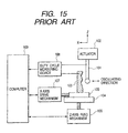
- Fig. 15 shows a first conventional arrangement represented by the unexamined Japanese patent application No. Kokai 5-264214.
- a probe 101 when actuated by an actuator 102, oscillates in a direction shown by an arrow.
- the probe 101 is placed closely to a measuring object 103.
- the measuring object 103 is mounted on an X stage 105 which is shiftable in the X-axis direction.
- the X stage 105 is mounted on a Z stage 104 which is shiftable in the Z-axis direction.
- the Z stage 104 is connected to and driven by a Z-axis feed mechanism 106.
- the X stage 105 is connected to and driven by an X-axis feed mechanism 107.
- a duty cycle measuring device 108 interposed between the probe 101 and the measuring object 103, measures the duty cycle.
- a computer 109 controls the Z-axis feed mechanism 106, the X-axis feed mechanism 107, and the duty cycle measuring device 108.
- the actuator 102 causes the probe 101 to oscillate at a predetermined position with a constant amplitude as shown by the arrow in Fig. 15. Electrical conduction between the probe 101 and the measuring object 103 is detectable as short-circuit current measured when a DC voltage is applied between the probe 101 and the measuring object 103.
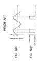
- the duty cycle measuring device 108 detects the ratio of a conductive duration to the oscillation period.
- Fig. 16A when the oscillating probe 101 exceeds a certain displacement "s" as shown in Fig. 16A, the electrically conductive condition is maintained between the probe 101 and the measuring object 103 as shown in Fig. 16B.
- Fig. 17 shows a relationship between the measured duty cycle and the relative distance between the probe 101 and the measuring object 103.
- the obtained relationship is not completely proportional. It is, however, possible to improve the proportionality when the sine wave in the oscillation of the probe 101 is changed to a triangular wave.
- the X-axis drive mechanism 107 is controlled to re-position the measuring object 103 for the measurement of the surface configuration of the measuring object 103.
- a second conventional arrangement is based on the AFM (scanning-type atomic force microscope) techniques which have been rapidly developed and applicable to the micro configuration measurement.
- AFM scanning-type atomic force microscope
- the unexamined Japanese patent application No. Kokai 6-323845 discloses an advanced AFM probe having a simplified structure and applicable to the micro configuration measurement for mechanical parts, whereas many of conventional AFM systems require a large-scale optical system to detect an interatomic force acting on the probe.
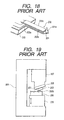
- FIGs. 18 and 19 show the schematic arrangement of the second conventional arrangement.
- a probe 201 is made of an elastic filmy plate of SiO 2 or the like whose size is 200 ⁇ 300 ⁇ m in length, 40 ⁇ 50 ⁇ m in width, and 1.8 ⁇ m in thickness.
- a pointed tip 201a made of ZnO whiskers, is bonded at the distal end of the probe 201.
- the probe 201 is provided on the surface of a silicon wafer 203.
- Fig. 19 shows a practical arrangement of a measuring apparatus using the above-described probe 201.
- a sample 206 is placed on a base body 204 via a Z-axis shift mechanism 205.
- the probe 201 is attached to the base body 204 via an XYZ piezoelectric scanner 207 and a piezoelectric plate 208 as shown in the drawing.
- the piezoelectric plate 208 causes the probe 201 to oscillate at its resonance frequency.
- the sample 206 approaches the pointed tip 201a of the probe 201 so closely that the oscillating condition of the probe 201 is significantly influenced by an interatomic force.
- a distortion signal detectable by the piezoelectric film 202b, has the amplitude and phase variable in response to the detected oscillation.
- the position of the XYZ piezoelectric scanner 207 in the Z-axis direction is controlled so as to maintain the changes in the amplitude and phase of the distortion signal, thereby detecting the surface configuration of the sample 206.
- the AFM detection mode is roughly classified into a contact mode (tapping mode) and a non-contact mode, as introduced in the journal of society of precision engineering, Vol. 62, No. 3, 1996, pp.345 ⁇ 350.
- the non-contact mode is a measurement mode preferable in that no damage is given to the surface of the sample. However, an absorbing layer, such as water on the sample surface, gives adverse influence in this measurement mode. Thus, the measurement is performed in the vacuum.
- the tapping mode is free from such problems derived from the absorbing layer.
- the AFM measurement according to this mode is generally performed in the air and is, therefore, applicable to the micro configuration measurement for many of mechanical parts.
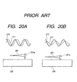
- Figs. 20A and 20B cooperatively show the principle of the contact detection in the tapping mode.
- the piezoelectric film 202b detects a distortion waveform 211 of the probe 201 whose phase is delayed 90° with respect to the exciting waveform 210 of the probe 201.
- the pointed tip 201a is brought into contact with the sample 206.
- the oscillation of the probe 201 is restricted so as to cause the distortion waveform 211 varied in the amplitude.
- the configuration of the sample 206 is thus measured based on the amplitude change of the distortion waveform 211.
- the detection of contact condition basically relies on the electrical conduction between the probe 101 and the measuring object 103.
- this measuring method is not applicable to the non-conductive members.
- the measuring object is electrically conductive, the measurement accuracy will be deteriorated by oxide films covering the surface or dusts on the surface.
- measuring objects are not limited to the ordinary AFM measuring objects, such as semiconductor surfaces or vacuum processed samples.
- AFM measuring objects such as semiconductor surfaces or vacuum processed samples.
- oily or dusty parts will contaminate the AFM probe 201 and render the measurement useless.
- Hard or rigid parts will abrade the probe 201.
- the measuring object when its surface has large undulation, may damage the probe.
- a micro surface measuring apparatus as defined in the preamble of claim 1 is disclosed in JP-A-6-323845.
- a 2-dimensional sampling of a semiconductor surface is provided.
- a horizontal objective surface is measured and the prove extends in a horizontal direction.
- the probe oscillates in a vertical direction and is positioned in a vertical direction.
- the probe is manufactured by a silicon process.
- the pointing tip of the probe is made of a Si-group material.
- the distortion detecting device of the probe is made by a piezoelectric material formed on the probe.
- JP-A-6-201315 A comparable apparatus is disclosed in JP-A-6-201315. With this known apparatus a non-contact distortion sensor is provided. Such a non-contact distortion sensor is not suitable for a micro hole because of interference between the sensor and a measured objective.
- the present invention has an object to provide a surface configuration measuring apparatus capable of measuring the micro surface configuration of mechanical parts.
- the present invention provides a micro surface measuring apparatus for measuring the configuration of an objective surface, said apparatus comprising: a probe having a cantilever structure; oscillating means for oscillating said probe, at or near its resonance frequency; distortion detecting means for detecting a distortion amount of said probe; positioning means for adjusting the position of said probe in an oscillating direction so as to stabilize the distortion amount at a constant value; and shifting means for adjusting the mutual position between said probe and the objective surface; said apparatus being characterized in that said probe has a cantilever structure extending in a vertical direction; in that said oscillating means are laid out for oscillating said probe in a horizontal direction; and in that rotary means are associated with said positioning means for changing the angular direction of said probe on a horizontal plane; whereby the configuration of said objective surface is detected based on the composite movement of said probe resulting from a three-dimensional motion of said shifting means and a rotational motion of said positioning means associated with said rotary means.
- a cemented carbide sintered hard alloy
- a piezoelectric ceramic supporting this probe, causes the probe to oscillate at or near its resonance frequency.
- the oscillating pointed tip When the oscillating pointed tip is brought into contact with the surface of the measuring object, the oscillating probe has the amplitude and phase varying in accordance with the degree of the contact.
- a piezoelectric ceramic, provided on the probe produces a distortion signal reflecting the distortion derived from the contact between the probe and the measuring object. The servo positioning of the probe is performed so as to stabilize at least one of the amplitude and the phase of the distortion signal.
- the probe is shifted along the surface of the measuring object while maintaining a relative distance between the probe and the measuring object.
- the probe moves along the surface of the measuring object. It becomes possible to measure the configuration of the measuring object.
- the present invention realizes a micro surface configuration measuring apparatus capable of stably measuring the surface of a measuring object regardless of its conductiveness, not adversely influenced by the oxide film or dusts on the surface, with a probe which is highly resistive in abrasion, highly stable in shape, and highly durable in corrosion.
- the present invention provides a micro surface measuring apparatus for measuring the configuration of an objective surface, the apparatus comprising a probe having a cantilever structure, oscillating means for oscillating the probe at or near its resonance frequency, distortion detecting means for detecting a distortion amount of the probe, positioning means for adjusting the position of the probe in an oscillating direction so as to stabilize the distortion amount at a constant value, and shifting means for adjusting the mutual position between the probe and the objective surface.
- the probe has a pointed tip measuring the configuration of the objective surface and made of a conductive member which is high in hardness.
- the probe is made of a cemented carbide which is highly resistive in abrasion, highly stable in shape, and highly durable in corrosion.
- the configuration measurement for mechanical parts can be stably performed under actual environments.
- the probe is partially or entirely made of a diamond or BN (boron nitride) sintered material which is harder than the cemented carbide. This is effective to enhance the resistivity in abrasion and the stability in shape.
- the configuration measurement for mechanical parts can be stably performed under actual environments.
- the probe is manufactured by a micro electric discharge machining. It becomes possible to flexibly form the probe in various shape.
- a deteriorated layer formed during the micro electric discharge machining is removed off by the abrasive grain processing. It becomes possible to obtain the probe highly stable in shape.
- the oscillating means includes a piezoelectric member supporting the probe. This provides a stable arrangement for supporting the probe stably.
- the oscillating means includes a piezoelectric member provided on the probe. This is effective to simplify the probe arrangement.
- the distortion detecting means includes a piezoelectric member provided on the probe.
- the distortion detecting means includes a strain gauge provided on the probe.
- the displacement of the probe is adjustable so as to stabilize a phase variation and/or an amplitude variation based on the comparison between a signal obtained from the distortion detecting means and a drive signal of the oscillating means. This realizes a quick and smooth feedback or servo control for positioning the probe.
- the stable configuration measurement can be realized.
- a voltage is applied between the probe and the objective surface to detect electric characteristics of the objective surface based on a current value measured between the probe and the objective surface.
- the probe and the objective surface are magnetic members, and the probe includes a coil to detect the magnetic characteristics of the objective surface based on a magnetic flux density modified in accordance with the oscillation of the probe.
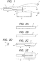
- Fig. 1 is a side view showing the probe arrangement in accordance with a preferable embodiment of the present invention.
- a probe 1 is configured into a stepped cantilever arrangement, with a pointed tip 1a at its distal end.
- the probe 1 has a beam portion 1b and a proximal portion 1c integrally arranged from the pointed tip 1a in this order.
- a piezoelectric plate 2 extends along the upper surface of the probe 1 in the region from the beam portion 1b to the proximal portion 1c.
- the probe 1 is supported on a support table 4 via a piezoelectric element 3 which is provided below the proximal portion 1c.
- a distortion amount of the piezoelectric plate 2 is detectable through a preamplifier 5.
- a high-voltage amplifier 6 drives the piezoelectric element 3 fixed on the support table 4.
- the probe 1 oscillates in an oscillating direction 7.
- the oscillation frequency is substantially identical with the resonance frequency of the beam portion 1b of the probe 1.
- the piezoelectric plate 2 detects the oscillation of the beam portion 1b.
- the pointed tip 1a of the probe 1 approaches the objective surface of a measuring object so closely that they are brought into contact with each other at periodic intervals.
- the configuration of the objective surface of the measuring object can be detected according to the principle of the AFM tapping mode.
- the probe 1 is made of a cemented carbide (sintered hard alloy) so that the piezoelectric element 3 can effectively resonate the probe 1.
- the cemented carbide is very hard, anti-frictional, highly elastic, and anti-corrosive.
- the properties of the cemented carbide is suitable for the probe used for measuring the configuration of the measuring object.
- the cemented carbide is generally difficult to machine due to its hardness.
- the present invention adopts a micro electric discharge machining.
- the cemented carbide is a sintered member, it is not subjected to the deformation processing or plastic working. This is preferable in that the cemented carbide has a small or negligible internal stress and is applicable to the micro machining.
- the cemented carbide can be replaced by a tool steel or a thermet which is also used as a tool material, or by a stainless steel or other metallic (e.g., tungsten) materials.
- the configuration measurement may be influenced by its anti-frictional or anti-corrosive properties which are inferior to those of the cemented carbide.
- Figs. 2A to 2E are views showing practical processes for manufacturing the probe 1 by using the micro electric discharge machining.
- a thin plate material 1' serving as the probe 1
- This thin plate material 1' is formed by grinding a cemented carbide.
- Another thin plate material 2' serving as the piezoelectric plate 2 has a thickness of 20 ⁇ 30 ⁇ m.
- the thin plate material 2' is formed by sintering the green sheet of PZT.
- the area of the thin plate material 2' is substantially identical with that (10 mm ⁇ 2 mm) of the thin plate material 1'.
- silver electrodes are formed on the opposed surfaces of the thin plate material 2'.
- the thin plate material 2' of the piezoelectric plate 2 is securely bonded on the surface of the thin plate material 1' of the probe 1 by using an electrically conductive adhesive.
- Fig. 2B only the thin plate material 2' is processed by the dicing machine to have a thickness of 50 ⁇ m. More specifically, by precisely adjusting the cutting depth of the grindstone, only the thin plate material 2' is planed while the cemented carbide plate is left without being processed.
- the reason why the piezoelectric plate 2 needs to be processed independently prior to the machining of the cemented carbide plate is that the piezoelectric plate 2 cannot be processed by the micro electric discharge machining due to its non-conductiveness.
- the thin plate material 1' is processed by the micro electric discharge machining into the probe 1 with the pointed tip 1a at its distal end and the beam portion 1b.
- the pointed tip 1a has a sharp edge with the curvature radius of approximately 1 ⁇ m, configured by the micro electric discharge machining.
- Fig. 2D is a left side view showing the fabricated probe 1 with the piezoelectric plate 2.
- Fig. 2E is a plan view showing the fabricated probe 1 with the piezoelectric plate 2.
- the beam portion 1b is so thin that it can be inserted in an inside space of a microstructural member.
- the width of the beam portion 1b is 70 ⁇ m.
- the proximal portion 1c is wider than the beam portion 1b so that the proximal portion 1c can be easily installed on the support table 4 via the piezoelectric element 3.
- the width of the proximal portion 1c is 2 mm.
- the thickness of the beam portion 1b is 50 ⁇ m. While the thickness of the proximal portion 1c is 500 ⁇ m. In the bending rigidity, there is a large difference equivalent to three digits between the beam portion 1b and the proximal portion 1c. In other words, the beam portion 1b can be regarded as a cantilever.
- a n a coefficient variable in accordance with the order of the oscillation
- I an areal second moment of the beam portion 1b
- m 1 the mass of the beam portion 1b per unit length.
- the probe 1 may be completely made of a cemented carbide whose Young's modulus is 6.4 ⁇ 10 2 Gpa and the density ⁇ is 1.4 ⁇ 10 3 kg/m 3 .
- the primary resonance frequency f 1 becomes 24 kHz when the length of the beam portion 1b is 1.5 mm.
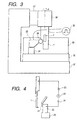
- Fig. 3 shows the micro electric discharge machining apparatus which performs the machining processes explained with reference to Figs. 2A to 2E.
- the micro electric discharge machining apparatus shown in Fig. 3 is based on the model MG-ED (commercially available from Matsushita Electric Industrial Co., Ltd.).
- the apparatus comprises a base 31, an XY stage 32 mounted on the base 31, a machining tank 33 mounted on the XY stage 32.
- the machining tank 33 stores the machining fluid.
- the machining tank 3 is provided with a wire guide 35 mounted on a support 34.
- a brass wire 36 which is 100 ⁇ m in diameter and held at the distal end of the wire guide 35, serves as an electrode for machining the thin plate material 1' into the probe 1.
- the probe 1 is partly dipped into the machining fluid stored in the machining tank 33.
- the portion to be processed is disposed adjacent to the wire 36.
- the base 31 supports the probe 1 via a Z stage 37 and a rotary table 38.
- the thin plate material 2' of the piezoelectric plate 2 mounted on the thin plate material 1' of the probe 1, is already machined in the predetermined shape.
- a power source 39 is connected between the thin plate material 1' and the wire 36 held on the wire guide 35.
- a voltage of the power source 39 is applied to a gap between the thin plate material 1' and the wire 36.
- the wire 36 wears significantly due to the electric discharge energy during the machining of the thin plate material 1'.
- the electric discharge machining is performed according to the so-called WEDG method which attains the machining accuracy of a sub ⁇ m level.
- the rotary table 38 accurately adjusts the angle of the thin plate material 1' in accordance with advancement of the electric discharge machining.
- the XY stage 32 and the Z stage 37 cooperate to adjust the positional relationship between the thin plate material 1' and the wire 36 during the electric discharge machining.
- the electric discharge machining basically utilizes the thermal energy of electric discharge to remove or cut the material.
- a deteriorated layer remains on the processed material.
- the processed surface of the cemented carbide usually lacks the bonding phase because the Co metal in the bonding phase has a low melting point while the WC powders serving as the main material have a high melting point. In this deteriorated condition, the WC powders are easily removed off the processed surface. If such a cemented carbide with a deteriorated surface is directly used for the probe 1, the pointed tip of the probe 1 will be deformed during the measurement. This results in errors in the measurement.
- the plate 1 is brought into contact with the surface of a metallic wear plate 22.
- a slurry 21 containing abrasive grain is applied on the surface of the wear plate 22 as shown in Fig. 4.
- an oscillation generator 23 can generate the oscillatory movement of 50 Hz in frequency and 5 ⁇ m in amplitude in an arbitrary direction.
- the wear plate 22 is made of a relatively soft material, such as tin or copper.
- a current detecting circuit including a DC power source 24, an ammeter 25, and a resister 26, is connected between the probe 1 and the wear plate 22 to detect the contact condition between the probe 1 and the wear plate 22.
- the positioning mechanism performs the positioning operation for the probe 1 in accordance with the current value measured by the ammeter 25.
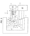
- Fig. 5 is a schematic view showing an overall arrangement of the micro surface configuration measuring apparatus equipped with the probe 1.
- a base 41 mounts an X stage 42, a Y stage 43, and a Z stage 44 in this order.
- a main CPU 45 controls these stages 42 to 44.
- a measuring object 46 is placed on the top of the stacked stages 42 to 44 so that it is shiftable in a three-dimensional space.
- the accuracy in the positioning the stages 42 to 44 directly leads to the error in the configuration measurement.
- This embodiment uses a built-in linear scale for accurately managing the position of each stage.
- the main CPU 45 controls a rotary table 47 provided at an upper portion of the base 41.
- An actuator 48 is attached to the rotary table 47.
- the probe 1 with the piezoelectric plate 2 is attached to the actuator 48 via the support table 4 and the piezoelectric element 3.
- the actuator 48 moves in the direction 7 identical with the oscillating direction of the piezoelectric element 3.
- the accuracy of the actuator 48 in the positioning operation is in the order of 1/100 ⁇ m. Its dynamic range is as wide as the movable range of 100 ⁇ m.
- the arrangement of this embodiment comprises both the piezoelectric element and a displacement enlargement mechanism. As the actuator 48 is attached to the rotary table 47, the oscillating direction 7 of the probe 1 is variable in 360°.
- the roundness of the rotary table 47 gives influence to the error in the configuration measurement.
- the rotary table 47 uses an air bearing which is highly accurate.
- a signal, representing a distortion of the piezoelectric plate 2 is sent from the piezoelectric plate 2 to a sub CPU 51 via the preamplifier 5 and an orthogonal detector 49.
- the sub CPU 51 generates a command voltage signal sent to the piezoelectric element 3 via a VCO 50 and the high-voltage amplifier 5.
- the piezoelectric element 3 causes the oscillatory movement.
- the sub CPU 51 not only controls the actuator 48 but also sends a signal to the main CPU 45.
- the signal generated from the VCO 50 is sent to the orthogonal detector 49, too.
- the probe 1 it is generally difficult to shift the probe 1 to a measuring point on the measuring object 46 by simply relying on the naked eyes. This is why a microscope 54 is equipped for the alignment.
- the measuring object 46 is shifted under the microscope 54 by the X stage 42 so that the coordinates of the measuring point can be measured through the microscopic screen displaying the measuring object 46. Using the measured coordinates, the measuring point can be accurately positioned under the probe 1.
- the above-described micro surface configuration measuring apparatus operates in the following manner.
- the VCO 50 generates a constant frequency signal based on the command voltage signal fed from the sub CPU 51.
- the constant frequency signal is sent to the piezoelectric element 3 via the high-voltage amplifier 6.
- the piezoelectric element 3 oscillates in the direction 7. This oscillatory movement is transmitted to the probe 1.
- the piezoelectric plate 2 produces the distortion signal which is entered into the orthogonal detector 49 via the preamplifier 5.
- the orthogonal detector 49 measures a phase shift between the distortion signal and the output signal of the VCO 50.
- the measured phase shift is sent to the sub CPU 51.
- the output frequency of the VCO 50 is set to a predetermined value so that the probe 1 can cause the resonant oscillation.
- the 90° phase difference is provided between the output signal of the preamplifier 5 and the output signal of the VCO 50.
- the resonance frequency being set in this embodiment, is approximately 25 kHz.
- any change in the phase and/or amplitude reflects the contact condition of the probe 1.
- the amplitude of the oscillation is approximately 100 nm at the distal end of the probe 1.
- the force f required for causing a distortion of 100 nm is approximately 3 mg.
- filmy water existing on the surface of the measuring object may cause a measuring error due to its surface tension.
- an appropriate arrangement (not shown) is provided for supplying dry air to the surface of the measuring object so as to remove the water or moisture component from the surface of the measuring object.
- the condition of the probe 1 slightly deviates from the resonant oscillation. This deviation is detectable as an output of the orthogonal detector 49 and is sent to the sub CPU 51.
- the sub CPU 51 controls the actuator 48 to correct or eliminate this deviation.
- the probe 1 can be always shifted along the surface of measuring object 46 while maintaining a negligible clearance therebetween.
- the configuration of the measuring object is detectable from the composite movement resulting from the three-dimensional motion of the stages 42 to 44 and the rotational motion of the actuator 48 mounted on the rotary table 47.
- the signal sent from the sub CPU 51 to the main CPU 45 is a signal representing the position of the actuator 48.
- the main CPU 45 manages all of the position data of the stages 42 to 44 and the rotary table 47, it is possible for the main CPU 45 to perform necessary calculations based on the position data and display the measuring result.
- the apparatus shown in Fig. 5 includes a current detecting circuit comprising a DC power source 52 and an ammeter 53. Although it is dispensable for the configuration measurement, providing this circuit makes it possible to know the electric properties of the objective surface, such as local oxidation, dirt or stain, or locally deteriorated conductivity, based on the current measured by the ammeter 53. This electric measurement can be done simultaneously with the configuration measurement.
- the measuring object 46 is made of a magnetic member.
- a magnetic circuit is formed between the measuring object 46 and the probe 1 which is a ferromagnetic substance. It is preferable to provide a coil wound around the proximal portion 1c of the probe 1. The magnetic flux, when modified by the oscillation of the probe 1, can be measured by this coil. If the ferromagnetism of the probe 1 gives adverse influence to the measurement, it will be possible to obtain a non-magnetic probe by modifying the material of the bonding phase of the cemented carbide.
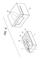
- Fig. 6 shows the method for installing the probe to the micro surface configuration measuring apparatus.
- the probe used in the micro surface measuring apparatus of this embodiment, is a mechanical cantilever whose length is limited within a certain range in view of the strength in comparison with its thickness.
- the probe needs to be thin and short enough for measuring a thin hole, on the other hand, needs to be thick and long enough for measuring a deep place.
- a plurality of probes are prepared beforehand and selectively used in accordance with the measuring object. Therefore, it is important to provide a simplified attaching and/or detaching arrangement for exchanging the probes.
- the support table 4 is a ceramic flat plate. Electrodes 80, 81 and 82 are formed on the upper surface of this support table 4.
- the electrode 80 is directly connected to a lower electrode (not shown) of the piezoelectric element 3.
- electric power is supplied to the electric electrode 80.
- the electrode 81 is grounded to maintain an upper electrode (not shown) of the piezoelectric element 3 and the probe 1 at a ground potential.
- the electrode 82 connected to the piezoelectric plate 2, serves as an output terminal of the distortion signal obtained from the piezoelectric plate 2.
- a socket 85 has a receiving bore which faces downward when the socket 85 is fixed to the actuator 48 of the micro surface configuration measuring apparatus.
- the probe 1 is attached to the socket 85 by inserting the support table 4 into the receiving bore of the socket 85.
- the electrodes 80, 81 and 82 formed on the surface of the support table 4 are brought into contact with corresponding electrodes 83 formed in the receiving bore when the support table 4 is completely engaged with the socket 85.
- the electrodes 80, 81 and 82 are electrically connected to other electric components of the micro surface configuration measuring apparatus.
- the socket 85 is equipped with a lock mechanism (not shown) for securely holding the support table 4.
- the manufacturing cost of the probe may not be low according to the manufacturing method disclosed in the above-described embodiment, because this manufacturing method includes the bonding of the piezoelectric material onto the probe material as well as the machining of both the piezoelectric material and the probe member.
- the following embodiment provides a non-expensive manufacturing method.
- a prepared probe material 1" is grinding finished.
- This probe material 1" is 0.2 mm in thickness and has a square shape of 20 mm ⁇ 20 mm.
- a piezoelectric plate material 2' having substantially the same size as that of the probe material 1", is bonded on the surface of the probe material 1" in a face-to-face relationship.
- Silver electrodes (not shown) are formed on opposed surfaces of the piezoelectric plate material 2'.
- the bonded unit of the materials 1" and 2' is then configured into the shape shown in Fig. 7B through the sand blasting.
- a plurality of piezoelectric plates 2 are formed on the surface of the probe material 1".
- the piezoelectric plate is subjected to the pressurized air.
- having a low aspect ratio is preferable.
- the minimum pattern size of the piezoelectric plate 2 is 200 ⁇ m.
- Fig. 7C is a plan view showing a plurality of divided probe materials 1' which are obtained by cutting the probe material 1" by the wire cut electric discharge machining.
- One piezoelectric plate 2 is mounted on each divided probe material 1'.
- the succeeding machining processes are identical with those explained with reference to Fig. 2, and performed so as to obtain the probes one after another.
- the piezoelectric plate 2 processed by the sand blasting has a width of 200 ⁇ m which is wider than that of the piezoelectric plate 2 processed by the dicing.
- the probe 1 has a wide portion 1d as part of the beam portion 1b.
- the length 1 and the thickness h of the probe 1 are the parameters determining the resonance frequency of the probe 1.
- the width b has no influence to the resonance frequency. Accordingly, providing the wide portion 1d gives no adverse influence to the properties of the probe 1.
- this embodiment makes it possible to perform the bonding process, the sandblasting, and the wire cut electric discharge machining for forming numerous probes.
- 10 to 20 probes can be batch processed at a time. This improves the manufacturing efficiency.
- the processes shown in Figs. 7D and 7E need to be done independently for each probe by using the micro electric discharge machining. This may be advantageous in that numerous kinds but small number of probe configurations can be provided to satisfy various measuring requirements from the users.
- the present invention provides various probe arrangements.
- Fig. 8A is a side view showing the probe material 1' of the probe 1.
- Fig. 8B is a side view showing the accomplished shape of the probe 1 fabricated from the probe material 1'.
- the probe material 1' comprises a cemented carbide 27 and a diamond layer 28 which are stacked and sintered together.
- the sintered diamond layer 28 has a bonding phase of cobalt.
- the electric discharge machining is preferably applied on the sintered diamond layer 28 to fabricate the probe 1 by using the method explained with reference to Figs. 2A ⁇ 2E or 7A ⁇ 7D.
- the fabricated probe 1 has a pointed tip 1a made of a sintered diamond.
- the pointed tip 1a has excellent anti-frictional property which is superior to that of the cemented carbide.
- the life of the probe can be extended greatly.
- the sintered diamond layer can be replaced by a sintered BN (boron nitride) having the metallic bonding phase.
- the beam portion 1b is made of the cemented carbide 27, it is possible to use a beam portion 1b made of a sintered diamond material. In this case, the beam portion 1b may have poor durability against an impact force. It is thus preferable that the probe has a sufficient thickness.
- Fig. 9A is a side view showing another arrangement of the probe 1.
- Fig. 9B is a plan view showing the same.
- a second piezoelectric plate 51 is bonded on a reverse surface of the probe 1.
- the second piezoelectric plate 51 is a substitute for the piezoelectric element 3.
- the piezoelectric element 3 can be omitted.
- the piezoelectric element 3 can be removed from the measuring loop. It is effective to prevent any measuring errors derived from the shape drift or thermal deformation of the piezoelectric element 3.
- the piezoelectric plate 2 As shown in Fig. 10, to eliminate measuring errors derived from the piezoelectric element 3, it is possible to use the piezoelectric plate 2 itself as a means for oscillating the probe 1. According to this arrangement, the piezoelectric plate 2 is connected to an impedance meter 62 to read the change in the impedance value which reflects the contact condition of the oscillating probe 1. However, according to this arrangement, the measuring sensitivity may deteriorate when the piezoelectric plate 2 is downsized with a thin thickness. Thus, it is preferable that the piezoelectric plate 2 has an area larger than 1 mm 2 .
- Fig. 11A is a side view showing another arrangement of the probe 1.
- Fig. 11B is a plan view of the same. According to this arrangement, the piezoelectric plate 2 is replaced by a strain gauge 61.
- the strain gauge 61 has substantially the same function as that of the piezoelectric plate 2.
- the strain gauge 61 may be a metallic type or a semiconductor type.
- Fig. 12A is a side view showing another arrangement of the probe 1.
- Fig. 12B is a plan view of the same. According to this arrangement, a piezoelectric thin film 71 is formed on a surface of the probe 1.
- the piezoelectric thin film 71 has substantially the same function as that of the piezoelectric plate 2.
- the piezoelectric thin film 71 can be manufactured by using the sol-gel method, introduced by K.R.Udayakumar et al. in FERROELECTRIC THIN FILM ULTRASONIC MICROMOTORS, IEEE, 1991 or by using the sputtering method introduced by T. KAMADA et al. in Mat. Res. Soc. Syp. Proc. Vol. 433, pp377 (1996).
- the lapping is applied on the surface of the probe 1 made of a cemented carbide to improve the surface roughness.
- a Pt/Ti layer is formed on the finished surface of the probe 1.
- the piezoelectric thin film 71 is formed on the Pt/Ti layer.
- the etching is applied on the piezoelectric thin film 71 to leave the necessary portion.
- a distortion detecting electrode 72 is formed on the piezoelectric thin film 71 for detecting the distortion.
- the thickness of the piezoelectric thin film 71 is 1 ⁇ 3 ⁇ m at maximum. There are some merits which are not obtained when the bulky piezoelectric plate 2 is used.
- the thickness of the piezoelectric thin film 71 is sufficiently thin compared with that of the probe 1, it becomes possible to prevent the probe from bending due to the bimorph effect induced by a thermal expansion difference between them.
- the pattern forming by the etching makes it possible to reduce the thickness of the piezoelectric thin film to the level of 10 ⁇ m. This is effective in miniaturizing the probe.
- this arrangement does not require the electrically conductive adhesive which is used in the above-described embodiment for bonding the bulky piezoelectric plate 2. The internal damping with respect to the vibration is reduced, while the Q value in the resonance of the probe is increased. Thus, the sensitivity in the detection of the probe can be improved.
- Figs. 13A and 13B show another probe arrangement in accordance with the present invention. According to this arrangement, two distortion detecting electrodes 72a and 72b are formed on the piezoelectric thin film 71.
- Fig. 13A is a left side view of the probe 1
- Fig. 13B is a plan view of the same.
- the probe 1 oscillates in the oscillating direction 7. It is expected that the probe 1 is brought into contact with the measuring object in the sensing direction 73. However, there is a possibility that the probe 1 may be brought into contact with the measuring object in another sensing direction 74. In this case, such an unexpected contact is detectable from the change occurring in the resonant condition.
- this arrangement uses two distortion detecting electrodes 72a and 72b which are separated from each other.
- the distortion detecting electrodes 72a and 72b cooperate to detect the twist of the beam portion 1b so as to identify the difference between the sensing directions 73 and 74.
- Fig. 14 shows another probe arrangement in accordance with the present invention.
- right-and-left electrodes 76 are provided in addition to upper-and-lower electrodes 75.
- An oscillator 78 supplies an exciting signal of frequency f1 between the upper-and-lower electrodes 75 to resonate the probe 1 in one sensing direction 73.
- Another oscillator 77 supplies an exciting signal of frequency f2 between the right-and-left electrodes 76 to resonate the probe 1 in the other sensing direction 74.
- the thickness and the width of the beam portion 1b are appropriately designed so that the resonance frequency of the beam portion 1b is differentiated in the sensing direction 73 and in the sensing direction 74.
- the distortion detecting signal obtained from the piezoelectric plate 2 is separable into two frequency components which are detected through two orthogonal detectors 49 (not shown) independently as signals representing the contact conditions in the sensing directions 73 and 74.
- two orthogonal detectors 49 (not shown) independently as signals representing the contact conditions in the sensing directions 73 and 74.
- An exciting signal of frequency f3 is applied between these electrodes to oscillate the beam portion 1b in the direction 79. With this arrangement, it becomes possible to independently detect the contact condition in the direction 79.
- the above-described probes can be incorporated in the micro surface configuration measuring apparatus explained in the above-described embodiment to measure the configuration of a measuring object.
- the present invention provides the probe having a cantilever structure and made of a cemented carbide.
- the probe has the pointed tip used for measuring the configuration of a measuring object.
- the piezoelectric element supports this probe and oscillates the probe at or near its resonance frequency.
- the piezoelectric plate provided on the surface of the probe, produces the distortion signal representing the distortion occurring on the probe.
- the actuator performs the feedback or servo control to adjust the position of the probe in the oscillating direction, thereby stabilizing the oscillatory condition of the probe.
- the position of the probe with respect to the measuring object is continuously changed by driving the stages and the rotary table.
- the probe moves along the undulated surface of the objective surface.
- the configuration of the measuring object is measured.
Landscapes
- Physics & Mathematics (AREA)
- Health & Medical Sciences (AREA)
- General Health & Medical Sciences (AREA)
- General Physics & Mathematics (AREA)
- Nuclear Medicine, Radiotherapy & Molecular Imaging (AREA)
- Radiology & Medical Imaging (AREA)
- Chemical & Material Sciences (AREA)
- Engineering & Computer Science (AREA)
- Nanotechnology (AREA)
- Analytical Chemistry (AREA)
- Crystallography & Structural Chemistry (AREA)
- Length Measuring Devices With Unspecified Measuring Means (AREA)
- Measurement Of Length, Angles, Or The Like Using Electric Or Magnetic Means (AREA)
Claims (13)
- Vorrichtung zur Vermessung von Mikrooberflächen zur Messung der Gestalt einer Objektivoberfläche, wobei die Vorrichtung umfasst: einen Fühler (1) mit einem Auslegeraufbau;
Schwingungsmittel (3), um den Fühler (1) bei oder nahe seiner Resonanzfrequenz in Schwingung zu versetzen;
Verzerrungsdetektionsmittel (48) zur Detektion eines Ausmaßes der Verzerrung des Fühlers;
Positioniermittel (48) zur Einstellung der Stellung des Fühlers in einer Schwingungsrichtung, um so das Ausmaß der Verzerrung bei einem konstanten Wert zu stabilisieren; und
Verschiebemittel (42 - 44) zur Einstellung der Stellung zwischen dem Fühler und der Objektivoberfläche zueinander;
dadurch gekennzeichnet, dass
der Fühler (1) einen Auslegeraufbau aufweist, der sich in einer vertikalen Richtung erstreckt;
die Schwingungsmittel (3) so ausgelegt sind, dass der Fühler (1) in einer horizontalen Richtung in Schwingung versetzt wird; und
Drehmittel (47) zu den Positioniermitteln (48) gehören, um die Winkelrichtung des Fühlers (1) auf einer horizontalen Ebene zu ändern;
wobei die Gestalt der Objektivoberfläche auf Basis der zusammengesetzten Bewegung des Fühlers (1) detektiert wird, die aus einer dreidimensionalen Bewegung der Verschiebemittel (42 - 44) und einer Drehbewegung der Positioniermittel (48), die zu den Drehmitteln (47) gehören, resultiert. - Vorrichtung zur Vermessung von Mikrooberflächen nach Anspruch 1, worin der Fühler (1) eine scharfe Spitze (1a) aufweist, welche die Gestalt der Objektivoberfläche vermisst und aus einem leitenden Element mit großer Härte hergestellt ist.
- Vorrichtung zur Vermessung von Mikrooberflächen nach Anspruch 1 oder 2, worin der Fühler (1) aus einem Sinterkarbid hergestellt ist.
- Vorrichtung zur Vermessung von Mikrooberflächen nach Anspruch 1 oder 2, worin der Fühler (1) teilweise oder vollständig aus einem Diamant- oder gesinterten BN-(Bomitrid-)Material hergestellt ist.
- Vorrichtung zur Vermessung von Mikrooberflächen nach einem der Ansprüche 1 bis 4, worin der Fühler (1) durch eine elektro-erosive Mikrobearbeitung hergestellt ist.
- Vorrichtung zur Vermessung von Mikrooberflächen nach einem der Ansprüche 1 bis 5, worin eine zerstörte Schicht, die während der elektro-erosiven Mikrobearbeitung gebildet wurde, durch Anwendung der Schleifkornbearbeitung entfernt wird.
- Vorrichtung zur Vermessung von Mikrooberflächen nach einem der Ansprüche 1 bis 6, worin das Schwingungsmittel ein piezoelektrisches Element (3) umfasst, welches den Fühler (1) trägt.
- Vorrichtung zur Vermessung von Mikrooberflächen nach einem der Ansprüche 1 bis 6, worin das Schwingungsmittel ein piezoelektrisches Element (51) umfasst, welches an dem Fühler vorgesehen ist.
- Vorrichtung zur Vermessung von Mikrooberflächen nach einem der Ansprüche 1 bis 8, worin das Verzerrungsdetektionsmittel ein piezoelektrisches Element (2) umfasst, welches an dem Fühler vorgesehen ist.
- Vorrichtung zur Vermessung von Mikrooberflächen nach einem der Ansprüche 1 bis 8, worin das Verzerrungsdetektionsmittel einen Dehnungsmesser (61) umfasst, welcher an dem Fühler vorgesehen ist.
- Vorrichtung zur Vermessung von Mikrooberflächen nach einem der Ansprüche 1 bis 10, worin die Verschiebung des Fühlers so einstellbar ist, dass eine Phasenschwankung und / oder eine Amplitudenschwankung auf Basis eines Vergleichs zwischen einem von dem Verzerrungsdetektionsmittel erhaltenen Signal und einem Ansteuerungssignal des Schwingungsmittels stabilisiert wird.
- Vorrichtung zur Vermessung von Mikrooberflächen nach einem der Ansprüche 1 bis 11, worin eine Spannung (52) zwischen dem Fühler und der Objektivoberfläche angelegt wird, um elektrische Eigenschaften der Objektivoberfläche auf Basis eines zwischen dem Fühler und der Objektivoberfläche gemessenen Stromwertes (53) zu detektieren.
- Vorrichtung zur Vermessung von Mikrooberflächen nach einem der Ansprüche 1 bis 12, worin der Fühler und die Objektivoberfläche magnetische Elemente sind, und der Fühler eine Spule umfasst, um die magnetischen Eigenschaften der Objektivoberfläche auf Basis einer in Übereinstimmung mit der Schwingung des Fühlers modifizierten magnetischen Flussdichte zu detektieren.
Applications Claiming Priority (4)
| Application Number | Priority Date | Filing Date | Title |
|---|---|---|---|
| JP1021998 | 1998-01-22 | ||
| JP1021998 | 1998-01-22 | ||
| JP30816498A JP3309816B2 (ja) | 1998-01-22 | 1998-10-29 | 微細表面形状測定装置及び触針製造方法 |
| JP30816498 | 1998-10-29 |
Publications (2)
| Publication Number | Publication Date |
|---|---|
| EP0932020A1 EP0932020A1 (de) | 1999-07-28 |
| EP0932020B1 true EP0932020B1 (de) | 2003-04-16 |
Family
ID=26345455
Family Applications (1)
| Application Number | Title | Priority Date | Filing Date |
|---|---|---|---|
| EP99101147A Expired - Lifetime EP0932020B1 (de) | 1998-01-22 | 1999-01-21 | Apparat zur Vermessung von Mikrooberflächen |
Country Status (4)
| Country | Link |
|---|---|
| US (2) | US6365895B1 (de) |
| EP (1) | EP0932020B1 (de) |
| JP (1) | JP3309816B2 (de) |
| DE (1) | DE69906835T2 (de) |
Families Citing this family (31)
| Publication number | Priority date | Publication date | Assignee | Title |
|---|---|---|---|---|
| KR100576898B1 (ko) * | 2001-01-29 | 2006-05-03 | 스미토모덴키고교가부시키가이샤 | 콘택트프로브 및 그 제조방법 및 검사장치 및 검사방법 |
| JP3481213B2 (ja) * | 2001-03-22 | 2003-12-22 | 日本電子株式会社 | 原子間力顕微鏡における試料観察方法および原子間力顕微鏡 |
| JP2004161444A (ja) * | 2002-11-14 | 2004-06-10 | Canon Inc | シート材判別装置 |
| EP1530220A1 (de) * | 2003-11-04 | 2005-05-11 | SwissProbe AG | Ausleger Anordnung |
| US7497133B2 (en) * | 2004-05-24 | 2009-03-03 | Drexel University | All electric piezoelectric finger sensor (PEFS) for soft material stiffness measurement |
| US9423693B1 (en) | 2005-05-10 | 2016-08-23 | Victor B. Kley | In-plane scanning probe microscopy tips and tools for wafers and substrates with diverse designs on one wafer or substrate |
| US7571638B1 (en) | 2005-05-10 | 2009-08-11 | Kley Victor B | Tool tips with scanning probe microscopy and/or atomic force microscopy applications |
| US7185440B2 (en) * | 2005-07-18 | 2007-03-06 | Seagate Technology Llc | Sensing contact probe |
| US7395698B2 (en) * | 2005-10-25 | 2008-07-08 | Georgia Institute Of Technology | Three-dimensional nanoscale metrology using FIRAT probe |
| JP2007322558A (ja) | 2006-05-30 | 2007-12-13 | Canon Inc | 水分量推定装置、シート材処理装置、水分量推定方法、及びシート材処理方法 |
| US7784107B2 (en) | 2006-06-02 | 2010-08-24 | Victor B. Kley | High speed measurement, analysis and imaging systems and methods for length scales from meter to sub-nanometer |
| US8481335B2 (en) * | 2006-11-27 | 2013-07-09 | Drexel University | Specificity and sensitivity enhancement in cantilever sensing |
| US7992431B2 (en) * | 2006-11-28 | 2011-08-09 | Drexel University | Piezoelectric microcantilevers and uses in atomic force microscopy |
| EP2100125A4 (de) | 2006-11-28 | 2012-02-15 | Univ Drexel | Piezoelektrische mikrocantilever-sensoren für biosensorik |
| JP2010518380A (ja) * | 2007-02-01 | 2010-05-27 | ドレクセル・ユニバーシティー | センサー用途向けハンドヘルド型位相シフト検出器 |
| EP1970714A1 (de) * | 2007-03-12 | 2008-09-17 | Capres Aps | Vorrichtung mit Kontaktdetektor |
| JP4937849B2 (ja) | 2007-07-03 | 2012-05-23 | 株式会社ミツトヨ | ステム製造方法およびステム製造装置 |
| KR100868029B1 (ko) * | 2007-07-10 | 2008-11-11 | 한국과학기술연구원 | 질감 측정 장치 및 그 방법 |
| JP5032235B2 (ja) * | 2007-08-02 | 2012-09-26 | 株式会社ミツトヨ | 共振センサの測定位置検出方法及び装置 |
| US8241569B2 (en) | 2007-11-23 | 2012-08-14 | Drexel University | Lead-free piezoelectric ceramic films and a method for making thereof |
| US8741663B2 (en) | 2008-03-11 | 2014-06-03 | Drexel University | Enhanced detection sensitivity with piezoelectric sensors |
| EP2101181A1 (de) | 2008-03-12 | 2009-09-16 | Capres A/S | Vorrichtung mit Kontaktdetektor |
| US8104093B2 (en) | 2008-03-28 | 2012-01-24 | Empire Technology Development Llc | Magnetic sensor and scanning microscope |
| EP2281192A4 (de) | 2008-05-16 | 2014-02-05 | Univ Drexel | System und verfahren zur gewebebeurteilung |
| US20110086368A1 (en) * | 2009-10-08 | 2011-04-14 | Drexel University | Method for immune response detection |
| US8722427B2 (en) * | 2009-10-08 | 2014-05-13 | Drexel University | Determination of dissociation constants using piezoelectric microcantilevers |
| JP5703155B2 (ja) * | 2011-07-14 | 2015-04-15 | 株式会社ミツトヨ | 接触式プローブおよびその製造方法 |
| US9778572B1 (en) | 2013-03-15 | 2017-10-03 | Victor B. Kley | In-plane scanning probe microscopy tips and tools for wafers and substrates with diverse designs on one wafer or substrate |
| JP2019100874A (ja) * | 2017-12-04 | 2019-06-24 | 株式会社ミツトヨ | 形状測定装置 |
| CN112964910A (zh) * | 2020-09-16 | 2021-06-15 | 中国科学院沈阳自动化研究所 | 原子力显微镜一体化双探针快速原位切换测量方法与装置 |
| US12569923B1 (en) | 2024-11-18 | 2026-03-10 | King Saud University | Micro-electric discharge milling machine with spark control |
Family Cites Families (11)
| Publication number | Priority date | Publication date | Assignee | Title |
|---|---|---|---|---|
| US5266801A (en) * | 1989-06-05 | 1993-11-30 | Digital Instruments, Inc. | Jumping probe microscope |
| US5403373A (en) | 1991-05-31 | 1995-04-04 | Sumitomo Electric Industries, Ltd. | Hard sintered component and method of manufacturing such a component |
| JPH0569324A (ja) | 1991-09-12 | 1993-03-23 | Mitsubishi Heavy Ind Ltd | 放電加工変質層の除去方法 |
| JP3261544B2 (ja) * | 1991-10-03 | 2002-03-04 | キヤノン株式会社 | カンチレバー駆動機構の製造方法、プローブ駆動機構の製造方法、カンチレバー駆動機構、プローブ駆動機構、及びこれを用いたマルチプローブ駆動機構、走査型トンネル顕微鏡、情報処理装置 |
| JP3069931B2 (ja) | 1992-03-16 | 2000-07-24 | 科学技術振興事業団 | 表面形状測定方法及び装置 |
| US5412980A (en) | 1992-08-07 | 1995-05-09 | Digital Instruments, Inc. | Tapping atomic force microscope |
| JP3131517B2 (ja) | 1992-12-25 | 2001-02-05 | オリンパス光学工業株式会社 | 走査型プローブ顕微鏡装置 |
| JPH06323845A (ja) | 1993-03-19 | 1994-11-25 | Tadatomo Suga | 走査型力顕微鏡用薄膜式力検出プローブ |
| US5559330A (en) * | 1993-12-20 | 1996-09-24 | Nippon Telegraph And Telephone Corporation | Scanning tunneling microscope |
| JPH08285512A (ja) | 1995-04-12 | 1996-11-01 | Matsushita Electric Ind Co Ltd | 微細表面形状測定装置 |
| JP3070499B2 (ja) * | 1996-11-26 | 2000-07-31 | 富士ゼロックス株式会社 | 微細切削方法および微細切削装置 |
-
1998
- 1998-10-29 JP JP30816498A patent/JP3309816B2/ja not_active Expired - Fee Related
-
1999
- 1999-01-20 US US09/233,484 patent/US6365895B1/en not_active Expired - Fee Related
- 1999-01-21 DE DE69906835T patent/DE69906835T2/de not_active Expired - Fee Related
- 1999-01-21 EP EP99101147A patent/EP0932020B1/de not_active Expired - Lifetime
-
2002
- 2002-02-01 US US10/060,365 patent/US6621080B2/en not_active Expired - Fee Related
Also Published As
| Publication number | Publication date |
|---|---|
| DE69906835D1 (de) | 2003-05-22 |
| DE69906835T2 (de) | 2004-01-29 |
| EP0932020A1 (de) | 1999-07-28 |
| US6621080B2 (en) | 2003-09-16 |
| JPH11271345A (ja) | 1999-10-08 |
| US6365895B1 (en) | 2002-04-02 |
| JP3309816B2 (ja) | 2002-07-29 |
Similar Documents
| Publication | Publication Date | Title |
|---|---|---|
| EP0932020B1 (de) | Apparat zur Vermessung von Mikrooberflächen | |
| EP0886758B1 (de) | Auslegerstrukturen | |
| JP4933775B2 (ja) | 微小表面形状測定プローブ | |
| US6267005B1 (en) | Dual stage instrument for scanning a specimen | |
| EP2084712B1 (de) | Sondenanordnung für ein rastersondenmikroskop | |
| US6193199B1 (en) | Sample stage including a slider assembly | |
| JP4528937B2 (ja) | 計測・加工システム | |
| Kim et al. | The vibroscanning method for the measurement of micro-hole profiles | |
| KR19990029072A (ko) | 내부 원자 측정 방법 | |
| JP5193337B2 (ja) | 微小表面形状測定プローブ | |
| KR100407202B1 (ko) | 원자표면또는다른파상표면을주사하는스캐닝터널링현미경의센서또는기타센서의나노미터단위의실시간위치측정방법및장치 | |
| Gao et al. | Experiments using a nano-machining instrument for nano-cutting brittle materials | |
| Yamamoto et al. | Dimensional measurement of high aspect ratio micro structures with a resonating micro cantilever probe | |
| JPH06258072A (ja) | 圧電体薄膜評価装置、原子間力顕微鏡 | |
| JP2725741B2 (ja) | 微小表面硬度測定装置 | |
| JPH08226928A (ja) | 光学顕微鏡付属型原子間力顕微鏡 | |
| JP2002107140A (ja) | 微細表面形状測定装置および触針製造方法 | |
| JPH11136968A (ja) | 超音波駆動装置 | |
| US20240118310A1 (en) | Device for measuring and/or modifying a surface | |
| JP2002154100A (ja) | 微細加工装置及び微細加工方法 | |
| Jeong et al. | Portable nano probe for micro/nano mechanical scratching and measuring | |
| JP2007240238A (ja) | プローブ顕微鏡およびプローブ顕微鏡の測定方法 | |
| JP2002283300A (ja) | 微細加工方法及び微細加工装置 | |
| JP2001174211A (ja) | 表面形状測定装置および測定方法 |
Legal Events
| Date | Code | Title | Description |
|---|---|---|---|
| PUAI | Public reference made under article 153(3) epc to a published international application that has entered the european phase |
Free format text: ORIGINAL CODE: 0009012 |
|
| 17P | Request for examination filed |
Effective date: 19990121 |
|
| AK | Designated contracting states |
Kind code of ref document: A1 Designated state(s): DE FR GB |
|
| AX | Request for extension of the european patent |
Free format text: AL;LT;LV;MK;RO;SI |
|
| 17Q | First examination report despatched |
Effective date: 20000201 |
|
| AKX | Designation fees paid |
Free format text: CY DE FR |
|
| RBV | Designated contracting states (corrected) |
Designated state(s): DE FR GB |
|
| GRAG | Despatch of communication of intention to grant |
Free format text: ORIGINAL CODE: EPIDOS AGRA |
|
| RTI1 | Title (correction) |
Free format text: MICRO SURFACE MEASURING APPARATUS |
|
| GRAG | Despatch of communication of intention to grant |
Free format text: ORIGINAL CODE: EPIDOS AGRA |
|
| GRAH | Despatch of communication of intention to grant a patent |
Free format text: ORIGINAL CODE: EPIDOS IGRA |
|
| GRAH | Despatch of communication of intention to grant a patent |
Free format text: ORIGINAL CODE: EPIDOS IGRA |
|
| GRAA | (expected) grant |
Free format text: ORIGINAL CODE: 0009210 |
|
| AK | Designated contracting states |
Designated state(s): DE FR GB |
|
| REG | Reference to a national code |
Ref country code: GB Ref legal event code: FG4D |
|
| REF | Corresponds to: |
Ref document number: 69906835 Country of ref document: DE Date of ref document: 20030522 Kind code of ref document: P |
|
| ET | Fr: translation filed | ||
| PLBE | No opposition filed within time limit |
Free format text: ORIGINAL CODE: 0009261 |
|
| STAA | Information on the status of an ep patent application or granted ep patent |
Free format text: STATUS: NO OPPOSITION FILED WITHIN TIME LIMIT |
|
| 26N | No opposition filed |
Effective date: 20040119 |
|
| PGFP | Annual fee paid to national office [announced via postgrant information from national office to epo] |
Ref country code: GB Payment date: 20070117 Year of fee payment: 9 |
|
| PGFP | Annual fee paid to national office [announced via postgrant information from national office to epo] |
Ref country code: DE Payment date: 20070118 Year of fee payment: 9 |
|
| PGFP | Annual fee paid to national office [announced via postgrant information from national office to epo] |
Ref country code: FR Payment date: 20070109 Year of fee payment: 9 |
|
| GBPC | Gb: european patent ceased through non-payment of renewal fee |
Effective date: 20080121 |
|
| PG25 | Lapsed in a contracting state [announced via postgrant information from national office to epo] |
Ref country code: DE Free format text: LAPSE BECAUSE OF NON-PAYMENT OF DUE FEES Effective date: 20080801 |
|
| REG | Reference to a national code |
Ref country code: FR Ref legal event code: ST Effective date: 20081029 |
|
| PG25 | Lapsed in a contracting state [announced via postgrant information from national office to epo] |
Ref country code: GB Free format text: LAPSE BECAUSE OF NON-PAYMENT OF DUE FEES Effective date: 20080121 |
|
| PG25 | Lapsed in a contracting state [announced via postgrant information from national office to epo] |
Ref country code: FR Free format text: LAPSE BECAUSE OF NON-PAYMENT OF DUE FEES Effective date: 20080131 |