EP0932189A2 - Structure d'une inductance utilisant de l'air comme diélectrique - Google Patents
Structure d'une inductance utilisant de l'air comme diélectrique Download PDFInfo
- Publication number
- EP0932189A2 EP0932189A2 EP99300479A EP99300479A EP0932189A2 EP 0932189 A2 EP0932189 A2 EP 0932189A2 EP 99300479 A EP99300479 A EP 99300479A EP 99300479 A EP99300479 A EP 99300479A EP 0932189 A2 EP0932189 A2 EP 0932189A2
- Authority
- EP
- European Patent Office
- Prior art keywords
- photoresist layer
- layer
- over
- patterned
- portions
- Prior art date
- Legal status (The legal status is an assumption and is not a legal conclusion. Google has not performed a legal analysis and makes no representation as to the accuracy of the status listed.)
- Withdrawn
Links
Images








Classifications
-
- H—ELECTRICITY
- H10—SEMICONDUCTOR DEVICES; ELECTRIC SOLID-STATE DEVICES NOT OTHERWISE PROVIDED FOR
- H10D—INORGANIC ELECTRIC SEMICONDUCTOR DEVICES
- H10D1/00—Resistors, capacitors or inductors
- H10D1/20—Inductors
-
- H—ELECTRICITY
- H01—ELECTRIC ELEMENTS
- H01F—MAGNETS; INDUCTANCES; TRANSFORMERS; SELECTION OF MATERIALS FOR THEIR MAGNETIC PROPERTIES
- H01F17/00—Fixed inductances of the signal type
- H01F17/0006—Printed inductances
-
- H—ELECTRICITY
- H10—SEMICONDUCTOR DEVICES; ELECTRIC SOLID-STATE DEVICES NOT OTHERWISE PROVIDED FOR
- H10W—GENERIC PACKAGES, INTERCONNECTIONS, CONNECTORS OR OTHER CONSTRUCTIONAL DETAILS OF DEVICES COVERED BY CLASS H10
- H10W20/00—Interconnections in chips, wafers or substrates
- H10W20/01—Manufacture or treatment
- H10W20/071—Manufacture or treatment of dielectric parts thereof
- H10W20/072—Manufacture or treatment of dielectric parts thereof of dielectric parts comprising air gaps
-
- H—ELECTRICITY
- H10—SEMICONDUCTOR DEVICES; ELECTRIC SOLID-STATE DEVICES NOT OTHERWISE PROVIDED FOR
- H10W—GENERIC PACKAGES, INTERCONNECTIONS, CONNECTORS OR OTHER CONSTRUCTIONAL DETAILS OF DEVICES COVERED BY CLASS H10
- H10W20/00—Interconnections in chips, wafers or substrates
- H10W20/40—Interconnections external to wafers or substrates, e.g. back-end-of-line [BEOL] metallisations or vias connecting to gate electrodes
- H10W20/45—Interconnections external to wafers or substrates, e.g. back-end-of-line [BEOL] metallisations or vias connecting to gate electrodes characterised by their insulating parts
- H10W20/46—Interconnections external to wafers or substrates, e.g. back-end-of-line [BEOL] metallisations or vias connecting to gate electrodes characterised by their insulating parts comprising air gaps
Definitions
- This invention relates generally to inductor structures and manufacturing methods and more particularly to spiral inductors adapted for use in monolithic microwave integrated circuits.
- active devices such as transistors
- passive devices such as resistors, capacitors and inductors
- a common single crystal substrate such as gallium arsenide (GaAs)
- GaAs gallium arsenide
- One technique used to form the inductor has been to: first form the active devices in the gallium arsenide, deposit a passivation layer of silicon nitride over the processed gallium arsenide, and pattern a layer of photoresist deposited over the silicon nitride layer with a spiral shaped window formed therein. Next, a sequence of titanium followed by gold is deposited over the photoresist layer and through the spiral shaped window onto the exposed portions of the silicon nitride. The photoresist layer is then removed, i.e., "lifted-off", leaving a spiral shaped inductor on the silicon nitride passivation layer.
- the inductor has a relatively low impedance resulting in a relatively narrow bandwidth device.
- an inductor structure is provided.
- the inductor has a dielectric body.
- a spiral shaped pedestal is disposed in one surface of the body.
- a ground plane conductor is disposed over an opposite surface of the body.
- a spiral shaped conductor is disposed over the spiral shaped dielectric pedestal.
- a method for making an inductor structure. The method includes the steps of: providing a dielectric body; patterning a metalization layer disposed over the dielectric body into a spiral shaped electrical conductor; etching surface portions of the dielectric body exposed by the patterned metalization layer providing a pedestal structure disposed under the patterned metalisation layer.
- a third photoresist layer is deposited over the formed surface.
- a window is formed in the third photoresist layer over the patterned metalization layer. Exposed portions of the passivation layer are removed. Exposed portions of the dielectric body are removed using a dry, vertically directional etch to produce an inductive structure.
- a single crystal substrate 10, here semi-insulating gallium arsenide is shown having a doped layer 12 of gallium arsenide epitaxially grown over the upper surface of the substrate 10.
- the epitaxial layer 12 may be formed active devices, such as field effect transistors, while an inductor structure 100 (FIGS. 6, 6A, 6B, 6C and 6D) is formed in a manner to be described in the region shown.
- a first photoresist layer 16, here polymethylglutarimide (PMGI) is formed over the passivation layer 14.
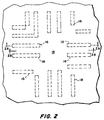
- the first photoresist layer 16 is selectively masked with unmasked portions being exposed to deep ultra-violent light in a conventional manner to form, after development, a segmented spiral shaped pattern as shown more clearly in FIG. 1.
- a second photoresist layer 18, here Novolac is deposited over the patterned first photoresist layer 16 and over portions of the passivation layer 16 exposed by the patterned first photoresist layer 16.
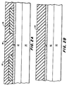
- the second photoresist layer 18 is masked and exposed to a less deep ultra-violet light to pattern it with a spiral shaped window disposed over and in vertical alignment with the segmented first photoresist layer 16, as shown in FIGS. 3, 3A and 3B.
- the window formed in the second photoresist layer is in the same shape as the spiral shaped inductor being formed.
- an electrical contact pad will be formed in the central region 22 of the inductor and a window is thus formed in the second photoresist layer 18 in the shape of the contact pad.
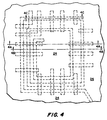
- a metalization layer 24 here a composite lower layer of titanium followed by a thicker layer of gold, is formed over the second photoresist 18 and through the window formed therein onto the patterned first photoresist layer 16 and onto the exposed portions of the passivation layer 14, as shown in FIGS 4, 4A, 4B and 4C.
- the second photoresist layer 18, together with the portions of the metalization layer 24 disposed thereon are removed (i.e., "lifted-off") with acetone leaving a spiral shaped metalization layer, as shown in FIGS. 5, 5A, 5B, 5C and 5D.
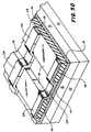
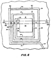
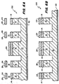
- the first photoresist layer 16 is removed here using n-methyl pyrolidinone, as shown in FIGS. 6, 6A, 6B, 6C and 6D to provide air-bridged segments 29 which pass over air 31, as shown.
- a third photoresist layer not shown, here Novolac is spun over the formed surface.
- a window is formed in the third photoresist layer over the patterned metalization layer 24.
- the exposed portions of the passivation layer 14 are removed, here using a dry etch, here a plasma etch using nitrogen tri-fluoride.
- exposed portions of the single crystal body 10 are etched here using a dry, vertically directional etch of tetrachloride or boron tri-chloride, for example, to provide the structure shown in FIGS. 6, 6A, 6B, 6C and 6D.
- a ground plane conductor 30 is disposed on the bottom surface of the substrate 10 to provide the inductor structure 100 shown in FIGS. 6, 6A, 6B, 6C and 6D.
- an inductor structure is formed in the single crystal body with a spiral shaped pedestal disposed in the upper surface of the body.
- the body is a dielectric body having a ground plane conductor disposed over a lower surface and a spiral shaped conductor disposed is disposed over the spiral shaped pedestal. Portions of The conductor are separated from underlying portions of the pedestal by air and laterally adjacent portions of the conductor are separated by air.
- dielectric may be material other than semiconductor material.
Landscapes
- Engineering & Computer Science (AREA)
- Power Engineering (AREA)
- Microelectronics & Electronic Packaging (AREA)
- Coils Or Transformers For Communication (AREA)
- Semiconductor Integrated Circuits (AREA)
Priority Applications (1)
| Application Number | Priority Date | Filing Date | Title |
|---|---|---|---|
| EP08075521A EP1975989A3 (fr) | 1998-01-22 | 1999-01-22 | Procédé de fabrication d'une structure d'inducteur |
Applications Claiming Priority (2)
| Application Number | Priority Date | Filing Date | Title |
|---|---|---|---|
| US12083 | 1998-01-22 | ||
| US09/012,083 US6169320B1 (en) | 1998-01-22 | 1998-01-22 | Spiral-shaped inductor structure for monolithic microwave integrated circuits having air gaps in underlying pedestal |
Related Child Applications (1)
| Application Number | Title | Priority Date | Filing Date |
|---|---|---|---|
| EP08075521A Division EP1975989A3 (fr) | 1998-01-22 | 1999-01-22 | Procédé de fabrication d'une structure d'inducteur |
Publications (2)
| Publication Number | Publication Date |
|---|---|
| EP0932189A2 true EP0932189A2 (fr) | 1999-07-28 |
| EP0932189A3 EP0932189A3 (fr) | 2002-10-09 |
Family
ID=21753312
Family Applications (2)
| Application Number | Title | Priority Date | Filing Date |
|---|---|---|---|
| EP99300479A Withdrawn EP0932189A3 (fr) | 1998-01-22 | 1999-01-22 | Structure d'une inductance utilisant de l'air comme diélectrique |
| EP08075521A Withdrawn EP1975989A3 (fr) | 1998-01-22 | 1999-01-22 | Procédé de fabrication d'une structure d'inducteur |
Family Applications After (1)
| Application Number | Title | Priority Date | Filing Date |
|---|---|---|---|
| EP08075521A Withdrawn EP1975989A3 (fr) | 1998-01-22 | 1999-01-22 | Procédé de fabrication d'une structure d'inducteur |
Country Status (2)
| Country | Link |
|---|---|
| US (2) | US6169320B1 (fr) |
| EP (2) | EP0932189A3 (fr) |
Cited By (1)
| Publication number | Priority date | Publication date | Assignee | Title |
|---|---|---|---|---|
| EP1264349A4 (fr) * | 2000-03-17 | 2007-11-07 | Robert Bruce Davies | Surface de fixation de puce comportant des bornes destinees a recevoir des composants et procede d'utilisation de cette fixation |
Families Citing this family (16)
| Publication number | Priority date | Publication date | Assignee | Title |
|---|---|---|---|---|
| US6542379B1 (en) * | 1999-07-15 | 2003-04-01 | International Business Machines Corporation | Circuitry with integrated passive components and method for producing |
| US6452247B1 (en) * | 1999-11-23 | 2002-09-17 | Intel Corporation | Inductor for integrated circuit |
| SG98398A1 (en) * | 2000-05-25 | 2003-09-19 | Inst Of Microelectronics | Integrated circuit inductor |
| FR2812755B1 (fr) * | 2000-08-04 | 2002-10-31 | St Microelectronics Sa | Inductance integree |
| US6774743B2 (en) | 2000-11-09 | 2004-08-10 | Merrimac Industries, Inc. | Multi-layered spiral couplers on a fluropolymer composite substrate |
| US6765455B1 (en) * | 2000-11-09 | 2004-07-20 | Merrimac Industries, Inc. | Multi-layered spiral couplers on a fluropolymer composite substrate |
| US7148553B1 (en) | 2001-08-01 | 2006-12-12 | Davies Robert B | Semiconductor device with inductive component and method of making |
| US6759275B1 (en) * | 2001-09-04 | 2004-07-06 | Megic Corporation | Method for making high-performance RF integrated circuits |
| JP3755453B2 (ja) * | 2001-11-26 | 2006-03-15 | 株式会社村田製作所 | インダクタ部品およびそのインダクタンス値調整方法 |
| US7022287B2 (en) * | 2002-05-08 | 2006-04-04 | Sandia National Laboratories | Single particle electrochemical sensors and methods of utilization |
| US20050086780A1 (en) * | 2003-10-23 | 2005-04-28 | Chartered Semiconductor Manufacturing Ltd. | Method of fabricating circular or angular spiral MIM capacitors |
| US7255801B2 (en) * | 2004-04-08 | 2007-08-14 | Taiwan Semiconductor Manufacturing Company, Ltd. | Deep submicron CMOS compatible suspending inductor |
| CN1901161B (zh) * | 2005-07-22 | 2010-10-27 | 米辑电子股份有限公司 | 连续电镀制作线路组件的方法及线路组件结构 |
| US20110223208A1 (en) | 2010-03-09 | 2011-09-15 | Beth Hill | Non-Aqueous High Concentration Reduced Viscosity Suspension Formulations |
| US9888568B2 (en) | 2012-02-08 | 2018-02-06 | Crane Electronics, Inc. | Multilayer electronics assembly and method for embedding electrical circuit components within a three dimensional module |
| US9230726B1 (en) | 2015-02-20 | 2016-01-05 | Crane Electronics, Inc. | Transformer-based power converters with 3D printed microchannel heat sink |
Family Cites Families (17)
| Publication number | Priority date | Publication date | Assignee | Title |
|---|---|---|---|---|
| US4729510A (en) * | 1984-11-14 | 1988-03-08 | Itt Corporation | Coaxial shielded helical delay line and process |
| JPS61144052A (ja) | 1984-12-17 | 1986-07-01 | Mitsubishi Electric Corp | 半導体装置 |
| JPH0377360A (ja) * | 1989-08-18 | 1991-04-02 | Mitsubishi Electric Corp | 半導体装置 |
| US5410179A (en) * | 1990-04-05 | 1995-04-25 | Martin Marietta Corporation | Microwave component having tailored operating characteristics and method of tailoring |
| US5550068A (en) * | 1990-11-05 | 1996-08-27 | Nippon Telegraph And Telephone Corporation | Process of fabricating a circuit element for transmitting microwave signals |
| US5336921A (en) * | 1992-01-27 | 1994-08-09 | Motorola, Inc. | Vertical trench inductor |
| JP2969025B2 (ja) | 1992-06-29 | 1999-11-02 | 毅 池田 | ノイズ・フィルタ |
| CA2154357C (fr) * | 1993-02-04 | 2004-03-02 | Kevin A. Shaw | Microstructures et methode a un seul masque et a cristal unique pour leur obtention |
| US5370766A (en) * | 1993-08-16 | 1994-12-06 | California Micro Devices | Methods for fabrication of thin film inductors, inductor networks and integration with other passive and active devices |
| JP3267049B2 (ja) * | 1994-05-25 | 2002-03-18 | 株式会社村田製作所 | エアブリッジ配線を有するスパイラルインダクタの製造方法 |
| JPH0936312A (ja) * | 1995-07-18 | 1997-02-07 | Nec Corp | インダクタンス素子およびその製造方法 |
| US5760456A (en) * | 1995-12-21 | 1998-06-02 | Grzegorek; Andrew Z. | Integrated circuit compatible planar inductors with increased Q |
| JP2904086B2 (ja) * | 1995-12-27 | 1999-06-14 | 日本電気株式会社 | 半導体装置およびその製造方法 |
| US6492705B1 (en) * | 1996-06-04 | 2002-12-10 | Intersil Corporation | Integrated circuit air bridge structures and methods of fabricating same |
| US5773870A (en) * | 1996-09-10 | 1998-06-30 | National Science Council | Membrane type integrated inductor and the process thereof |
| US5915188A (en) * | 1997-12-22 | 1999-06-22 | Motorola, Inc. | Integrated inductor and capacitor on a substrate and method for fabricating same |
| US6008102A (en) * | 1998-04-09 | 1999-12-28 | Motorola, Inc. | Method of forming a three-dimensional integrated inductor |
-
1998
- 1998-01-22 US US09/012,083 patent/US6169320B1/en not_active Expired - Lifetime
-
1999
- 1999-01-22 EP EP99300479A patent/EP0932189A3/fr not_active Withdrawn
- 1999-01-22 EP EP08075521A patent/EP1975989A3/fr not_active Withdrawn
-
2000
- 2000-11-02 US US09/704,892 patent/US6258652B1/en not_active Expired - Lifetime
Cited By (1)
| Publication number | Priority date | Publication date | Assignee | Title |
|---|---|---|---|---|
| EP1264349A4 (fr) * | 2000-03-17 | 2007-11-07 | Robert Bruce Davies | Surface de fixation de puce comportant des bornes destinees a recevoir des composants et procede d'utilisation de cette fixation |
Also Published As
| Publication number | Publication date |
|---|---|
| EP1975989A3 (fr) | 2009-06-03 |
| EP1975989A2 (fr) | 2008-10-01 |
| US6258652B1 (en) | 2001-07-10 |
| US6169320B1 (en) | 2001-01-02 |
| EP0932189A3 (fr) | 2002-10-09 |
Similar Documents
| Publication | Publication Date | Title |
|---|---|---|
| EP1975989A2 (fr) | Procédé de fabrication d'une structure d'inducteur | |
| US5812364A (en) | Capacitor | |
| US20020050626A1 (en) | Semiconductor device and manufacturing method therefor | |
| US5166096A (en) | Process for fabricating self-aligned contact studs for semiconductor structures | |
| US6239684B1 (en) | High-Q inductive elements | |
| US5583739A (en) | Capacitor fabricated on a substrate containing electronic circuitry | |
| US6232647B1 (en) | Air gap with borderless contact | |
| EP0166983A2 (fr) | Procédé pour l'exposition sélective des parois latérales d'une rainure et l'application pour la formation d'un contact de substrat en siliciure métallique pour dispositifs isolés par rainures remplies d'un matériau diélectrique | |
| US5973910A (en) | Decoupling capacitor in an integrated circuit | |
| US5216282A (en) | Self-aligned contact studs for semiconductor structures | |
| US6383889B2 (en) | Semiconductor device having improved parasitic capacitance and mechanical strength | |
| US6440839B1 (en) | Selective air gap insulation | |
| US5109267A (en) | Method for producing an integrated circuit structure with a dense multilayer metallization pattern | |
| US5915188A (en) | Integrated inductor and capacitor on a substrate and method for fabricating same | |
| EP0540276A2 (fr) | Procédé de fabrication d'un contact auto-aligné | |
| US5006485A (en) | Method of manufacturing an intergrated circuit including steps for forming interconnections between patterns formed at different levels | |
| WO2002029865A2 (fr) | Procede de fabrication d'un composant a semi-conducteur et composant ainsi obtenu | |
| JPH0640591B2 (ja) | モノリシツク半導体構造とその製法 | |
| JPS60124967A (ja) | 集積回路構造体 | |
| KR100345516B1 (ko) | 고주파 집적회로 장치 및 그 제조 방법 | |
| KR100611474B1 (ko) | 반도체 소자의 인덕터 제조 방법 | |
| JP2001223331A (ja) | 半導体装置及びその製造方法 | |
| KR20010043405A (ko) | 반도체 디바이스 제조 방법 | |
| JPH08222694A (ja) | 半導体装置および半導体装置の製造方法 | |
| US20100133586A1 (en) | Heterojunction bipolar transistor and method of forming the same |
Legal Events
| Date | Code | Title | Description |
|---|---|---|---|
| PUAI | Public reference made under article 153(3) epc to a published international application that has entered the european phase |
Free format text: ORIGINAL CODE: 0009012 |
|
| AK | Designated contracting states |
Kind code of ref document: A2 Designated state(s): AT BE CH CY DE DK ES FI FR GB GR IE IT LI LU MC NL PT SE |
|
| AX | Request for extension of the european patent |
Free format text: AL;LT;LV;MK;RO;SI |
|
| PUAL | Search report despatched |
Free format text: ORIGINAL CODE: 0009013 |
|
| AK | Designated contracting states |
Kind code of ref document: A3 Designated state(s): AT BE CH CY DE DK ES FI FR GB GR IE IT LI LU MC NL PT SE |
|
| AX | Request for extension of the european patent |
Free format text: AL;LT;LV;MK;RO;SI |
|
| 17P | Request for examination filed |
Effective date: 20030317 |
|
| AKX | Designation fees paid |
Designated state(s): DE FR |
|
| 17Q | First examination report despatched |
Effective date: 20030714 |
|
| RAP1 | Party data changed (applicant data changed or rights of an application transferred) |
Owner name: RAYTHEON COMPANY |
|
| GRAP | Despatch of communication of intention to grant a patent |
Free format text: ORIGINAL CODE: EPIDOSNIGR1 |
|
| RIC1 | Information provided on ipc code assigned before grant |
Ipc: H01L 21/02 20060101ALI20120313BHEP Ipc: H01L 21/768 20060101ALI20120313BHEP Ipc: H01F 17/00 20060101AFI20120313BHEP |
|
| STAA | Information on the status of an ep patent application or granted ep patent |
Free format text: STATUS: THE APPLICATION IS DEEMED TO BE WITHDRAWN |
|
| 18D | Application deemed to be withdrawn |
Effective date: 20120807 |