EP0933683A2 - Verfahren zur Bildung eines Lackmusters unter Verwendung einer, aus Siliziumkarbid, optimierten Antireflexionsschicht - Google Patents
Verfahren zur Bildung eines Lackmusters unter Verwendung einer, aus Siliziumkarbid, optimierten Antireflexionsschicht Download PDFInfo
- Publication number
- EP0933683A2 EP0933683A2 EP99108501A EP99108501A EP0933683A2 EP 0933683 A2 EP0933683 A2 EP 0933683A2 EP 99108501 A EP99108501 A EP 99108501A EP 99108501 A EP99108501 A EP 99108501A EP 0933683 A2 EP0933683 A2 EP 0933683A2
- Authority
- EP
- European Patent Office
- Prior art keywords
- reflective layer
- film
- refractive index
- thickness
- forming
- Prior art date
- Legal status (The legal status is an assumption and is not a legal conclusion. Google has not performed a legal analysis and makes no representation as to the accuracy of the status listed.)
- Withdrawn
Links
Images
























Classifications
-
- H—ELECTRICITY
- H10—SEMICONDUCTOR DEVICES; ELECTRIC SOLID-STATE DEVICES NOT OTHERWISE PROVIDED FOR
- H10P—GENERIC PROCESSES OR APPARATUS FOR THE MANUFACTURE OR TREATMENT OF DEVICES COVERED BY CLASS H10
- H10P70/00—Cleaning of wafers, substrates or parts of devices
- H10P70/20—Cleaning during device manufacture
- H10P70/27—Cleaning during device manufacture during, before or after processing of conductive materials, e.g. polysilicon or amorphous silicon layers
- H10P70/273—Cleaning during device manufacture during, before or after processing of conductive materials, e.g. polysilicon or amorphous silicon layers the processing being a delineation of conductive layers, e.g. by RIE
-
- G—PHYSICS
- G03—PHOTOGRAPHY; CINEMATOGRAPHY; ANALOGOUS TECHNIQUES USING WAVES OTHER THAN OPTICAL WAVES; ELECTROGRAPHY; HOLOGRAPHY
- G03F—PHOTOMECHANICAL PRODUCTION OF TEXTURED OR PATTERNED SURFACES, e.g. FOR PRINTING, FOR PROCESSING OF SEMICONDUCTOR DEVICES; MATERIALS THEREFOR; ORIGINALS THEREFOR; APPARATUS SPECIALLY ADAPTED THEREFOR
- G03F7/00—Photomechanical, e.g. photolithographic, production of textured or patterned surfaces, e.g. printing surfaces; Materials therefor, e.g. comprising photoresists; Apparatus specially adapted therefor
- G03F7/004—Photosensitive materials
- G03F7/09—Photosensitive materials characterised by structural details, e.g. supports, auxiliary layers
- G03F7/091—Photosensitive materials characterised by structural details, e.g. supports, auxiliary layers characterised by antireflection means or light filtering or absorbing means, e.g. anti-halation, contrast enhancement
-
- G—PHYSICS
- G03—PHOTOGRAPHY; CINEMATOGRAPHY; ANALOGOUS TECHNIQUES USING WAVES OTHER THAN OPTICAL WAVES; ELECTROGRAPHY; HOLOGRAPHY
- G03F—PHOTOMECHANICAL PRODUCTION OF TEXTURED OR PATTERNED SURFACES, e.g. FOR PRINTING, FOR PROCESSING OF SEMICONDUCTOR DEVICES; MATERIALS THEREFOR; ORIGINALS THEREFOR; APPARATUS SPECIALLY ADAPTED THEREFOR
- G03F7/00—Photomechanical, e.g. photolithographic, production of textured or patterned surfaces, e.g. printing surfaces; Materials therefor, e.g. comprising photoresists; Apparatus specially adapted therefor
- G03F7/70—Microphotolithographic exposure; Apparatus therefor
- G03F7/70691—Handling of masks or workpieces
-
- H—ELECTRICITY
- H10—SEMICONDUCTOR DEVICES; ELECTRIC SOLID-STATE DEVICES NOT OTHERWISE PROVIDED FOR
- H10P—GENERIC PROCESSES OR APPARATUS FOR THE MANUFACTURE OR TREATMENT OF DEVICES COVERED BY CLASS H10
- H10P50/00—Etching of wafers, substrates or parts of devices
- H10P50/20—Dry etching; Plasma etching; Reactive-ion etching
- H10P50/26—Dry etching; Plasma etching; Reactive-ion etching of conductive or resistive materials
- H10P50/264—Dry etching; Plasma etching; Reactive-ion etching of conductive or resistive materials by chemical means
- H10P50/266—Dry etching; Plasma etching; Reactive-ion etching of conductive or resistive materials by chemical means by vapour etching only
- H10P50/267—Dry etching; Plasma etching; Reactive-ion etching of conductive or resistive materials by chemical means by vapour etching only using plasmas
- H10P50/268—Dry etching; Plasma etching; Reactive-ion etching of conductive or resistive materials by chemical means by vapour etching only using plasmas of silicon-containing layers
-
- H—ELECTRICITY
- H10—SEMICONDUCTOR DEVICES; ELECTRIC SOLID-STATE DEVICES NOT OTHERWISE PROVIDED FOR
- H10P—GENERIC PROCESSES OR APPARATUS FOR THE MANUFACTURE OR TREATMENT OF DEVICES COVERED BY CLASS H10
- H10P50/00—Etching of wafers, substrates or parts of devices
- H10P50/71—Etching of wafers, substrates or parts of devices using masks for conductive or resistive materials
-
- H—ELECTRICITY
- H10—SEMICONDUCTOR DEVICES; ELECTRIC SOLID-STATE DEVICES NOT OTHERWISE PROVIDED FOR
- H10P—GENERIC PROCESSES OR APPARATUS FOR THE MANUFACTURE OR TREATMENT OF DEVICES COVERED BY CLASS H10
- H10P76/00—Manufacture or treatment of masks on semiconductor bodies, e.g. by lithography or photolithography
- H10P76/20—Manufacture or treatment of masks on semiconductor bodies, e.g. by lithography or photolithography of masks comprising organic materials
- H10P76/204—Manufacture or treatment of masks on semiconductor bodies, e.g. by lithography or photolithography of masks comprising organic materials of organic photoresist masks
- H10P76/2041—Photolithographic processes
- H10P76/2042—Photolithographic processes using lasers
-
- H—ELECTRICITY
- H10—SEMICONDUCTOR DEVICES; ELECTRIC SOLID-STATE DEVICES NOT OTHERWISE PROVIDED FOR
- H10P—GENERIC PROCESSES OR APPARATUS FOR THE MANUFACTURE OR TREATMENT OF DEVICES COVERED BY CLASS H10
- H10P76/00—Manufacture or treatment of masks on semiconductor bodies, e.g. by lithography or photolithography
- H10P76/20—Manufacture or treatment of masks on semiconductor bodies, e.g. by lithography or photolithography of masks comprising organic materials
- H10P76/204—Manufacture or treatment of masks on semiconductor bodies, e.g. by lithography or photolithography of masks comprising organic materials of organic photoresist masks
- H10P76/2041—Photolithographic processes
- H10P76/2043—Photolithographic processes using an anti-reflective coating
-
- H—ELECTRICITY
- H10—SEMICONDUCTOR DEVICES; ELECTRIC SOLID-STATE DEVICES NOT OTHERWISE PROVIDED FOR
- H10W—GENERIC PACKAGES, INTERCONNECTIONS, CONNECTORS OR OTHER CONSTRUCTIONAL DETAILS OF DEVICES COVERED BY CLASS H10
- H10W20/00—Interconnections in chips, wafers or substrates
- H10W20/01—Manufacture or treatment
- H10W20/031—Manufacture or treatment of conductive parts of the interconnections
Definitions
- the present invention concerns a method of determining conditions for an anti-reflective layer, a method of forming an anti-reflective layer, a method of forming a resist pattern by using a novel anti-reflective layer and a method of forming a film.
- a condition of an anti-reflective layer for defining optical conditions such as a thickness and a refractive index condition, for example, reflection refractive index and absorption refractive index of an anti-reflective layer upon forming a resist pattern by exposing a photoresist on an anti-reflective layer formed on an underlying material by a monochromatic light, a method of forming the anti-reflective layer utilizing the above-mentioned method and a method of forming a resist pattern by using a novel anti-reflective layer, and a method of forming a film which can be used in the above mentioned method of forming the anti-reflective layer.
- optical conditions such as a thickness and a refractive index condition, for example, reflection refractive index and absorption refractive index of an anti-reflective layer upon forming a resist pattern by exposing a photoresist on an anti-reflective layer formed on an underlying material by a monochromatic light
- the present invention can be utilized suitably, for example, to a case of setting an anti-reflective layer disposed for preventing the standing wave effect when photolithography is used or a case of forming a resist pattern by using an anti-reflective layer when photolithography is used upon manufacturing, for example, electronic materials (such as semi conductor devices).
- a KrF excimer laser beam (248 nm) is used and a lens of about 0.37 to 0.42 NA is mounted in most advanced steppers (projection exposing machine) at present (for example, Nikon NSR 1505 EX1, Canon FPA 4500).
- steppers projection exposing machine
- research and development have been studied for design rule devices in a sub-half micron (0.5 um) region.
- a monochromatic light is used as an exposing optical source.
- a phenomenon referred to as a standing wave effect occurs.
- the standing wave is caused by occurrence of light interference in a resist film. That is, it is caused by interference between an incident light P and a reflection light R from the interface between a resist PR and a substrate S in the film of the resist RR (Fig. 18).
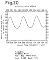
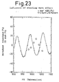
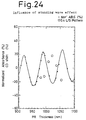
- the amount of light absorbed in the resist fluctuates depending on the thickness of the resist film (abscissa in the graph).
- the amount of light absorbed in the resist means an amount of light absorbed in the resist itself excluding the amount of light due to surface reflection, absorption by a metal if it is present in the resist, or light outgoing from the resist.
- the amount of the absorbed light constitutes an energy for causing light reaction to the resist.
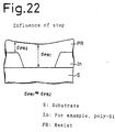
- the thickness of the resist film varies between upper and lower portions of the step. That is, the thickness dPR2 of the resist film on the protrusion In is smaller than the thickness dPR1 of the resist film in other portions than the above.
- the standing wave effect differs depending on the thickness of the resist film and, accordingly, fluctuation for the amount of the light absorbed in the resist changes respectively undergoing the effect of the standing wave effect.
- the dimension of the resist pattern obtained after exposure and development differs between the upper and the lower portions of the step.
- the dimensional accuracy of a resist pattern in a photolithographic step upon manufacturing a device such as a semiconductor device is generally ⁇ 5%. Although it is considered that an accuracy coarser than ⁇ 5% in total may be practically tolerable. However, it is desirable that the pattern accuracy upon resist exposure is within ⁇ 5%, if occurrence of scattering due to other factors such as focus is also taken into consideration. For attaining the dimensional accuracy of ⁇ 5%, it is essential to reduce the standing wave effect.
- Fig. 26 shows a dimensional variation of the resist pattern relative to the fluctuation (ordinate) for the amount of absorbed light in the resist film (abscissa).
- fluctuation for the amount of absorbed light in the resist film has to be within a range of less than 6% in order to manufacture, for example, a rule device of 0.35 um.
- the present invention has been achieved in view of the foregoing situations and it is an object thereof to provide a method of determining a condition for an anti-reflective layer capable of determining a condition of the anti-reflective layer used in a case of forming a resist pattern on an optional underlying material (substrate) by using an exposure optical source of an optional monochromatic light, so that a stable resist pattern can be formed satisfactorily even if the resist pattern is fine.
- Another object of the present invention is to provide a method of forming an anti-reflective layer by the condition described above.
- a further object of the present invention is to provide a method of forming a resist pattern by developing a novel anti-reflective layer and using such an anti-reflective layer.
- This method comprises determining a condition for an anti-reflective layer upon forming a resist pattern by exposing a photoresist on the anti-reflective layer formed on an underlying material by a monochromatic light, wherein the film thickness and the optical condition of the anti-reflective layer are determined by the following means, which comprises
- this method comprises forming an anti-reflective layer upon forming a photoresist pattern by exposing a photoresist on the anti-reflective layer formed on an underlying material by a monochromatic light, wherein the anti-reflective layer is formed by using a substance adaptable to the optical condition for the refractive index based on the optimum refractive index condition for the anti-reflective layer determined as optimum optical condition by the means (I) - (V) as defined in the first aspect.
- the method comprises forming a resist pattern which comprises forming an anti-reflective layer with silicon carbide on an underlying refractory metal silicide material and forming a photoresist on the anti-reflective layer.
- the method comprises forming a resist pattern by forming an anti-reflective layer on an underlying metalic material and forming a photoresist on the anti-reflective layer thereby forming a resist pattern, where in the anti-reflective layer is formed with an inorganic substance (SiC) under the conditions of the film thickness and the optical condition determined by the following means, which comprises:
- the method comprises forming a resist pattern which comprises forming an anti-reflective layer on an underlying metalic material with silicon carbide and forming a photoresist on the anti-reflective layer thereby, forming a resist pattern.
- the method comprises forming an anti-reflective layer on an underlying inorganic material (including metal material and silicon material) and forming a resist pattern on the anti-reflective layer thereby forming the resist pattern, wherein the anti-reflective layer is formed with an inorganic substance (SiC) satisfying the film thickness and the optical condition determined by the following means, which comprises:
- the method comprises forming a resist pattern which comprises forming an anti-reflective layer with silicon carbide on an underlying silicon material and forming a photoresist on the anti-reflective film, thereby forming a resist pattern.
- the method comprises forming a resist pattern as defined by the fourth aspect, wherein an anti-reflective layer is formed on an underlying metal material by using an inorganic substance (SiC) having a value within ⁇ 0.6 for the reflection refractive index n and a value within ⁇ 0.2 for the absorption refractive index k and forming a photoresist on the anti-reflective layer, thereby forming the resist pattern.
- SiC inorganic substance
- the method comprises forming a resist pattern as defined by the eighth aspect, wherein the underlying metalic material comprises a refractory metal silicide.
- the inventors have also developed a method of forming a resist pattern, in which a Si x O y N z film is formed as an anti-reflective layer on the underlying metalic material thereby forming a resist pattern.
- the metalic material is anyone of aluminum and aluminium alloys.
- the inventors have developed a method of forming a resist pattern in which a Si x O y N z or Si x N y film as an anti-reflective layer is formed on an underlying silicic material thereby forming a resist pattern.
- the silicic material comprises any one of single crystal silicon, polycrystalline silicon, amorphous silicon and doped poly-silicon.
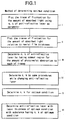
- the first aspect of the present invention comprises as shown in Fig. 1,
- An optimum condition for the anti-reflective layer is obtained in accordance with the foregoing constitution and a substance adaptable to the condition, that is, capable of satisfying or substantially satisfying such a condition is selected thereby enabling to form an effective anti-reflective layer.
- each of refractive indices n, k at each of specific wavelengths is determined by a means such as a spectroscopic ellipsometer and a substance having such refractive indices n, k is searched from existent substances as the anti-reflective material, or a substance for such a condition can be synthesized to serve for the anti-reflective material.
- the kind of the film that satisfies the condition to be met by the anti-reflective layer specified in (6) above is found by measuring the optical constant of each kind of the films by the exposure light. This corresponds to (V).
- an anti-reflective layer of an optimum condition can be formed in accordance with the condition obtained in (7) above and with the substance capable of satisfying the condition (corresponding to Fig. 1(VI)).
- the anti-reflective layer as an effective means for forming a stable fine pattern on an optional underlying material (substrate) by using a stepper having an optical source of an optional monochromatic light can be designed easily.
- the present invention can be utilized for finding a condition of an organic or inorganic film for forming an anti-reflective layer used for forming a stable resist pattern on a W-Si film by using a KrF excimer laser.
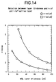
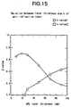
- a substance having n, k condition shown in Figs. 14 and 15 to be described later can be used.
- SiC constituting the anti-reflective layer can be formed by sputtering or CVD.
- SiC can also be etched by RIE using CF 4 , CHF 3 , C 2 F 6 , C 3 F 8 , SF 6 or NF 3 series gas as an etchant and by adding Ar to thereby improve ionic property.
- the third through eighth aspects of the present invention can be attained by conducting the operation for finding the substance capable of satisfying the condition as described above by using the above-mentioned method.
- SiC silicon carbide
- W-Si refractory metal silicide
- SiC constituting the anti-reflective layer can be formed by sputtering or CVD.
- SiC can be etched by RIE using CF 4 , CHF 3 , C 2 F 6 , C 3 F 8 , SF 6 or NF 3 gas as an etchant and by adding Ar to improve the ionic property.
- the concept of the first aspect is applied in a case of using a metalic material such as a refractory metal compound as the underlying material.
- SiC silicon carbide
- Al and Al-alloys material for example, Al, Al-Si, Al-Si-Cu or Cu and Cu-alloys material such as Cu, as well as that an organic or inorganic material found by the above-mentioned method is appropriate, based on which the present invention has been attained.
- This invention is preferably applied in a case of forming a stable resist pattern on an Al or al-alloys material such as Al, Al-Si or Al-Si-Cu or a Cu or Cu-alloys material such as Cu by using a KrF excimer laser.
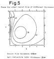
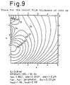
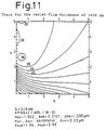
- an organic or inorganic substance having an optimum curve regarding the refractive index and the layer thickness of the anti-reflective layer obtained in (V) above, and within a range of the value on the curve ⁇ 0.2 for n and the value on the curve ⁇ 0.15 for k.
- SiO constituting the anti-reflective layer can be formed by CVD or thermal oxidation.
- SiC can be formed by sputtering or CVD.
- the anti-reflective layer can be etched by RIE using CF 4 , CHF 3 , C 2 F 6 , C 3 H 8 , SF 6 or NF 3 series gas as an etchant and adding Ar and O 2 to improve the ionic property.
- the concept of the first aspect is applied in a case of using an inorganic substance such as silicic material as an underlying material.
- SiC silicon carbide
- This invention can suitably be applied to a case of forming a stable resist pattern on a silicon substrate by using a KrF excimer layer.
- SiO constituting the anti-reflective layer can be formed, for example, by CVD or thermal oxidation.
- SiC can be formed, for example, by sputtering or CVD.
- the anti-reflective layer can be etched by RIE using CF 4 , CF 3 , C 2 F 6 , C 3 H 8 , SF 6 or NF 3 series gas as an etchant and adding Ar and O 2 or Ar or O 2 to improve the ionic property.
- SiO x film, SiO x N z film or S i N y film is appropriate on a metal material such as refractory metal silicide in accordance with the condition obtained by the method as described above.
- This invention is applicable preferably to a case of forming a stable resist pattern on a W-Si film by using a KrF excimer laser.
- a SiO x N y film is suitable on the underlying metalic material such as Al and Al-alloys material.
- SiO x N y film or Si x N y film is appropriate on the silicon series underlying material.
- the present invention is applied to determination of conditions to be satisfied by an anti-reflective layer (layer thickness, optical constant) for forming a stable pattern on a W-Si film by using KrF excimer lithography.
- an anti-reflective layer layer thickness, optical constant
- This example is practiced in accordance with the following steps (1) - (6).
- a film was formed by utilizing a thermal CVD process at a temperature of 100°C to 1500° and under a pressure of 0.01 to 10,000 Pa by using the following gas as the starting material gas:
- a film was formed by utilizing a plasma CVD process and using a photochemical reaction from a gas mixture comprising: Si 2 H 6 + Si(CH 3 ) H 3 + C 2 H 2 .
- a SiC film was formed as below to obtain an anti-reflective layer.
- a film was formed by utilizing an ECR plasma process and using a microwave (2.45 GHz) from a gas mixture comprising: SiH 4 + CH 4 + H 2 .
- a SiC film was formed as below to obtain an anti-reflective layer. That is, a film was formed by utilizing a sputtering method using SiC as a target.
- an anti-reflective layer was formed by patterning a SiC film by etching.
- the SiC film was etched by a reactive ion etching process using a CF 4 , CHF 3 , C 2 F 6 , C 3 F 8 , SF 6 or NF 3 series gas as an etchant and adding Ar to improve the ionic property, thereby obtaining an anti-reflective layer of a desired pattern.
- the present invention was applied by using SiC as an anti-reflective layer for forming a stable pattern on a W-Si film using KrF excimer lithography.
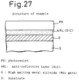
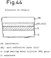
- an anti-reflective layer ARL was formed with silicon carbide on a W-Si underlying material which was a refractory metal silicide and a photoresist PR was formed on the anti-reflective layer ARL, thereby forming a resist pattern.
- the present invention is applied by using SiC as the anti-reflective layer ARC, particularly, in a case of forming a material layer with W-Si as a gate, on a substrate 1 such as a Si semiconductor substrate and patterning the same by a photolithographic step using a photoresist PR and an etching step, thereby obtaining a gate structure.
- a film was formed by utilizing a thermal CVD process at a temperature of 100°C to 1500° and under a pressure of 0.01 to 10,000 Pa by using the following gas as the starting material.
- a film was formed by utilizing a plasma CVD process and using a photochemical reaction for a gas mixture comprising: Si 2 H 6 + Si(CH 3 ) H 3 + C 2 H 2 .
- a SiC film was formed as blow to obtain an anti-reflective layer.
- a film was formed by utilizing an ECR plasma process and using a microwave (2.45 GHz) from a gas mixture comprising: SiH 4 + CH 4 + H 2 .
- a film was formed by utilizing an ECR plasma CVD process from SiH 4 + C 2 H 4 gas by a plasma process using a microwave at 2.45 GHz.
- a SiC film was formed as below to obtain an anti-reflective layer.
- a film was formed by a sputtering method using SiC as a target.
- an anti-reflective layer was formed by patterning a SiC film by etching.
- the SiC film was etched by a reactive ion etching process using CF 4 , CHF 3 , C 2 F 6 , C 3 F 8 , SF 6 or NF 3 series gas (or a mixed gas system) as an etchant and adding Ar to improve the ionic property, thereby obtaining an anti-reflective layer of a desired pattern.
- the present invention was applied by using SiC as the anti-reflective layer for forming a stable pattern on an Al, Al-Si or Al-Si-Cu film as the Al series material using KrF excimer lithography.
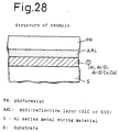
- an anti-reflective layer ARL was formed with silicon carbide on Al, Al-Si or Al-Si-Cu as an Al or Al-alloys metalic wiring material (1) and forming a photoresist PR on the anti-reflective layer ARL thereby forming a resist pattern.
- the present invention was applied, particularly, in a case of obtaining a wiring structure by forming a material layer as wiring with Al, Al-Si or Al-Si-Cu on a substrate S such as a Si semiconductor substrate, and patterning the same by a photolithographic step using the photoresist PR and an etching step, in which SiC was used as the anti-reflective layer ARC.
- Al-Si there can be preferably used, in addition to a generally used Al-Si alloy containing 1 wt% Si generally used, an alloy with lower or higher Si content. This example is preferably applicable to Al-Si-Cu in which Si is about 1 wt% and Cu is about 0.1 to 2 wt%, with no particular restriction only thereto.
- Al-Si-Cu alloy of 1 wt% Si, 0.5 wt% Cu is used.
- a film was formed by utilizing a thermal CVD process at a temperature of 100°C to 1500° and usually under a pressure, preferably, 0.01 to 10.000 Pa, more preferably, 100 to 10,000 Pa by using the following gas as the starting material gas:
- a SiC film was formed as below to obtain an anti-reflective layer. That is, in this example, a film was formed by utilizing a plasma CVD process and using a photochemical reaction in a gas mixture comprising: Si 2 H 6 + Si(CH 3 ) H 3 + C 2 H 2 .
- a SiC film was formed as below to obtain an anti-reflective layer.
- a film was formed by an ECR plasma process by utilizing an ECR plasma CVD process using a microwave (at 2.45 GHz) from a gas mixture comprising: SiH 4 + CH 4 + H 2 , SiH 4 + C 2 H 4 + H 2 or SiH 4 + CH 4 + H 2 .
- an SiC film was formed as below to obtain an anti-reflective layer, That is, a film was formed by utilizing a sputtering method using SiC as a target.
- an anti-reflective layer was formed by patterning a SiC film by etching.
- the SiC film was etched by a reactive ion etching process using a CF 4 , CHF 3 , C 2 F 6 , C 3 F 8 , SF 6 or NF 3 gas as an etchant and adding Ar to improve the ionic property, thereby obtaining an anti-reflective layer of a desired pattern.
- the present invention was applied by using SiO as an anti-reflective layer for forming a stable pattern on an Al, Al-Si or Al-Si-Cu film using KrF excimer lithography.
- an anti-reflective layer ARL was formed with silicon oxide SiO on an Al, Al-Si or Al-Si-Cu as the Al or Al-alloys metal wiring material and a photoresist PR was formed on the anti-reflective layer ARL, thereby forming the resist pattern.
- the present invention was applied by using SiO as the anti-reflective layer ARL, particularly, in a case of forming a material layer as wiring with Al, Al-Si or Al-Si-Cu on a substrate S such as a Si semiconductor substrate and patterning the same by a photolithographic step using a photoresist PR and an etching step, thereby obtaining a gate structure.
- a film was formed at a temperature from normal temperature to 500° and under a pressure of 0.01 to 10 Pa by using a gas mixture of SiH 4 + O 2 + N 2 .
- a SiO film having an aimed anti-reflective effect could be obtained.
- an anti-reflective layer was formed by patterning a SiO film by etching.
- the SiO film was etched by a reactive ion etching process using CF 4 , CHF 3 , C 2 F 6 , C 3 F 8 , SF 6 or NF 3 series gas (or a mixed gas system) as an etchant and adding Ar to improve the ionic property, thereby obtaining an anti-reflective layer of a desired pattern.
- an organic or inorganic substance suitable for forming a stable pattern on an Al, Al-Si or Al-Si-Cu film was obtained and using it as an anti-reflective layer by using KrF excimer lithography.
- an anti-reflective layer ARL was formed on Al, Al-Si or Al-Si-Cu as an Al or Al-alloys wiring material (1) and forming a photoresist PR on the anti-reflective layer ARL, thereby forming a resist pattern, in which an appropriate material was selected to form the anti-reflective layer.
- the anti-reflective layer was designed, particularly, in a case of obtaining a wiring structure by forming a material layer as wiring with Al, Al-Si or Al-Si-Cu on a substrate S such as a Si semiconductor substrate, and patterning the same by a photolithographic step using the photoresist PR and an etching step.
- the standing wave effect was reduced to less than ⁇ 3% by using an organic or inorganic substance capable of satisfying the optical property on the curve in Figs. 14 and 36, or within a range of a value on the curve ⁇ 0.2 for n and a value on the curve ⁇ 0.15 for k. Accordingly, such an organic or inorganic substance was determined to form an anti-reflective layer. As compared with the case of not using the anti-reflective layer, the standing wave effect was reduced to about 1/10.
- Cu wiring was formed by using Cu as the Cu or Cu-alloys material instead of the Al or Al-alloys metal material such as Al, Al-Si or Al-Si-Cu as the under-lying material in Examples 14 - 23 Embodiments 3 and 4, and an anti-reflective layer was formed thereon in the same manner as in each of the examples (SiC, SiO or an anti-reflective layer comprising an organic or inorganic substance determined by the same method as in Example 23 in a case where Cu was used as the under-lying material), thereby performing the resist patterning.
- the Al or Al-alloys metal material such as Al, Al-Si or Al-Si-Cu
- an anti-reflective layer was formed thereon in the same manner as in each of the examples (SiC, SiO or an anti-reflective layer comprising an organic or inorganic substance determined by the same method as in Example 23 in a case where Cu was used as the under-lying material), thereby performing the resist patterning.
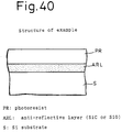
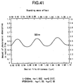
- the present invention was applied by using SiC as an anti-reflective layer for forming a stable pattern on a Si substrate using KrF excimer lithography.
- an anti-reflective layer ARL was formed with silicon carbide on a silicon substrate as the silicic underlying material and a photoresist PR was formed on the anti-reflective layer ARL, thereby forming the resist pattern.
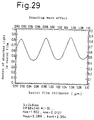
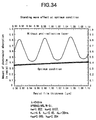
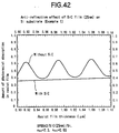
- Fig. 42 shows a comparison between a case of using SiC at 25 nm as the anti-reflective layer (graph for "with SiC") and a case of not using the anti-reflective layer (graph for "without SiC”).
- the standing wave effect was reduced to less than ⁇ 1%.
- the standing wave effect in the case of not using SiC was ⁇ 23%. Accordingly, the standing wave effect was reduced to less than 1/23 by using SiC as the anti-reflective layer on Si.
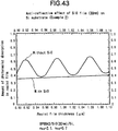
- Fig. 43 shows a comparison between a case of using SiO at 30 nm as the anti-reflective layer (graph for "with SiO") and a case of not using the anti-reflective layer (graph for "without SiO").
- the standing wave effect was about ⁇ 1%.
- the standing wave effect in the case of not using SiO was ⁇ 23%. Accordingly, the standing wave effect was reduced to less than about 1/23 by using SiC as the anti-reflective layer on Si.
- a film was formed by utilizing a thermal CVD process at a temperature of 100°C to 1500° and usually under a pressure, preferably, from 0.01 to 10,000 Pa, more preferably, 100 to 10,000 Pa by using the following gas as the starting material gas:
- an SiC film was formed as below to obtain an anti-reflective layer. That is, in this example, a film was formed by utilizing a plasma CVD process and using a photochemical reaction in a gas mixture comprising: Si 2 H 6 + Si(CH 3 ) H 3 + C 2 H 2 .
- a SiC film was formed as below to obtain an anti-reflective layer.
- a film was formed by an ECR plasma process by utilizing an ECR plasma CVD process using microwave (at 2.45 GHz) from a gas mixture comprising: SiH 4 + C 2 H 4 + H 2 , SiH 4 + C 2 H 4 + H 2 or SiH 4 + CH 4 + H 2 .
- a SiC film was formed as below to obtain an anti-reflective layer. That is, a film was formed by utilizing a sputtering method using SiC as a target.
- an anti-reflective layer was formed by patterning a SiC film by etching.
- the SiC film was etched by a reactive ion etching process using CF 4 , CHF 3 , C 2 F 6 , C 3 F 8 , SF 6 or NF 3 gas as an etchant and adding Ar to improve the ionic property, thereby obtaining an anti-reflective layer of a desired pattern.
- a film was formed by using a gas mixture of SiH 4 + O 2 + N 2 at a temperature from normal temperature to 500°C under a pressure of 0.01 Pa - 10 Pa.
- a gas mixture of SiH 4 + O 2 + N 2 at a temperature from normal temperature to 500°C under a pressure of 0.01 Pa - 10 Pa.
- the SiC layer and the SiO layer in each of the examples described above were formed on the underlying single crystal silicon, underlying polycrystalline silicon and underlying amorphous silicon, respectively, to form anti-reflective layers. As a result, a desired anti-reflective effect could be obtained to attain a satisfactory pattern formation.
- the present invention was applied by using SiO x as an anti-reflective layer for forming a stable pattern on a W-Si film using KrF excimer lithography.
- an anti-reflective layer ARL was formed with SiO x on an underlying W-Si material as refractory metal silicide and a photoresist PR was formed on the anti-reflective layer ARL, thereby forming the resist pattern.
- the present invention is applied by using SiO x as the anti-reflective layer ARL, particularly, in a case of forming a material layer as a gate with W-Si on a substrate 1 such as a Si semiconductor substrate and patterning the same by a photolithographic step using a photoresist PR and an etching step, thereby obtaining a gate structure.
- a film was formed by utilizing a parallel plate plasma CVD process and using a microwave (2.45 GHz) from a gas mixture of SiH 4 + O 2 .
- a film was formed by utilizing a parallel plate type plasma CVD process and using a microwave (2.45 GHz) from a gas mixture of SiH 4 + O 2 and using Ar as a buffer gas.
- a film was formed by utilizing an ECR type plasma CVD process and using a microwave (2.45 GHz) from a gas mixture of SiH 4 + O 2 .
- a film was formed by utilizing a ECR type plasma CVD process and using a microwave (2.45 GHz) from a gas mixture of SiH 4 + O 2 and using Ar as a buffer gas.
- a film was formed by utilizing a bias ECR plasma CVD process and using a microwave (2.45 GHz) from a gas mixture of SiH 4 + O 2 .
- a film was formed by utilizing a bias ECR type plasma CVD process and using a microwave (2.45 GHz) from a gas mixture of SiH 4 + O 2 and using Ar as a buffer gas.
- the SiO x film was etched by a reactive etching process using a gas system of CHF 3 (50 - 100 SCCM) + O 2 (3 - 20 SCCM) under a pressure of about 2 Pa and with a power of about 100 to 1000 W, to obtain a desired pattern by etching.
- the SiO x film was etched by a reactive etching process using a gas system of C 4 F 8 (30 - 70 SCCM) + CHF 3 (10 - 30 SCCM) under a pressure of about 2 Pa and with a power of about 100 to 1000 W, to obtain a desired pattern by etching.
- the SiO x film was etched by a reactive etching process using a gas system of S 2 F 2 (5 - 30 SCCM) under a pressure of about 2 Pa and with a power of about 100 to 1000 W, to obtain a desired pattern by etching.
- the present invention was applied by using a Si x O y N z or Si x N y film as an anti-reflective layer for forming a stable pattern on a W-Si film by using KrF excimer lithography.
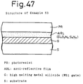
- an anti-reflective layer ARL was formed with Si x O y N z or Si x N y on the underlying W-Si as a refractory metal silicide and a photoresist PR was formed on the anti-reflective layer ARL, thereby forming the resist pattern.
- the present invention is applied by using Si x O y N z or Si x N y as the anti-reflective layer ARL, particularly, in a case of forming a material layer with W-Si as a gate on a substrate 1 such as a Si semiconductor substrate and patterning the same by a photolithographic step using a photoresist PR and an etching step, thereby obtaining a gate structure.
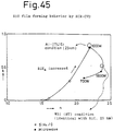
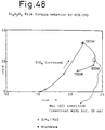
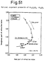
- the optical constant shows changes in Fig. 48 corresponding to the film forming conditions upon forming the Si x O y N z or Si x N y film by using the CVD process.
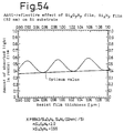
- Fig. 48 regions shown by open circles satisfy the conditions in Figs. 14 and 15. That is, Fig. 49 shows the standing wave effect in a case of using the Si x O y N z or Si x N y film at 25 nm thickness as an anti-reflective layer and in a case of not using the anti-reflective layer.
- the standing wave effect was about ⁇ 1.8% and the standing wave effect was reduced to less than about 1/12 as compared with the case of not using the anti-reflective layer.
- a film was formed by utilizing a parallel plate plasma CVD process, ECR plasma CVD process or bias ECR plasma CVD process, by using a microwave (2.45 GHz), from a gas mixture of SiH 4 + O 2 + N 2 or a gas mixture of SiH 4 + N 2 O.
- a film was formed by utilizing a parallel plate plasma CVD process, ECR plasma CVD process or bias ECR plasma CVD process, by using a microwave (2.45 GHz), from a gas mixture of SiH 4 + O 2 + N 2 or a gas mixture of SiH 4 + N 2 O and using Ar as a buffer gas.
- a film was formed by utilizing a parallel plate plasma CVD process, ECR plasma CVD process or bias ECR plasma CVD process, from a gas mixture of SiH 4 + O 2 + N 2 or a gas mixture of SiH 4 + N 2 O.
- a film was formed by utilizing a parallel plate plasma CVD process, ECR plasma CVD process or bias ECR plasma CVD process, from a gas mixture of SiH 4 + O 2 + N 2 or a gas mixture of SiH 4 + N 2 O and using Ar as a buffer gas.
- a film was formed by utilizing a parallel plate plasma CVD process, ECR plasma CVD process or bias ECR plasma CVD process, by using a microwave (2.45 GHz), from a gas mixture of SiH 4 + NH 3 or a gas mixture of SiH 2 Cl 2 + NH 3 .
- a film was formed by utilizing a parallel plate plasma CVD process, ECR plasma CVD process or bias ECR plasma CVD process, from a gas mixture of SiH 4 + O 2 or a gas mixture of SiH 2 Cl 2 + NH 3 and using Ar as a buffer gas.
- a film was formed by utilizing a parallel plate plasma CVD process, ECR plasma CVD process or bias ECR plasma CVD process, by using a microwave (2.45 GHz), from a gas mixture of SiH 4 + NH 3 or a gas mixture of SiH 2 CL 2 + NH 3 .
- a film was formed by utilizing a parallel plate plasma CVD process, ECR plasma CVD process or bias ECR plasma CVD process, from a gas mixture of SiH 4 + O 2 or a gas mixture of SiH 2 Cl 2 + NH 3 by using Ar as a buffer gas.
- the Si x O y N z or Si x N y film was etched by using a gas system of CHF 3 (50 - 100 SCCM) + O 2 (3 - 20 SCCM), under a pressure of about 2 Pa and with a power of about 100 - 1000 V by using a reactive etching process with improved ionic property, thereby etching a desired pattern.
- the Si x O y N z or Si x N y film was etched by using a gas system of C 4 F 8 (30 - 70 SCCM) + CHF 3 (10 - 30 SCCM), under a pressure of about 2 Pa and with a power of about 100 - 1000 V by using a reactive etching process with improved ionic property, thereby etching a desired pattern.
- the Si x O y N z or Si x N y film was etched by using a gas system of S 2 F 2 (5 - 30 SCCM), under a pressure of about 2 Pa and with a power of about 100 - 1000 V by using a reactive etching process with improved ionic property, thereby etching a desired pattern.
- the present invention was applied by using a Si x O y N z or Si x N y film as an anti-reflective layer for forming a stable resist pattern on an underlying Al, Al-Si or Al-Si-Cu material or on a silicon oxide film such as SiO 2 on the underlying material by using KrF excimer lithography.
- an anti-reflective layer ARL is formed with Si x O y N z or Si x N y on the underlying Al, Al-Si or Al-Si-Cu material as a metal wiring material, a photoresist PR was formed on the anti-reflective layer ARL or the photoresist PR was formed on the anti-reflective layer after forming a silicon oxide film such as SiO 2 on the anti-reflective layer to form a resist pattern.
- the present invention was applied by using Si x O y N z or Si x N y as the anti-reflective layer ARL, particularly, in a case of obtaining a wiring structure by forming a material layer as wiring with Al, Al-Si or Al-Si-Cu on a substrate such as a Si semiconductor substrate or forming a silicon oxide film such as SiO 2 on the material layer, which was then patterned by a photolithographic step using the photoresist PR and an etching step.
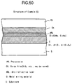
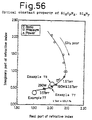
- an Si x O y N z film within a range of values on the curve in the graph showing the relation between the thickness of the anti-reflective layer and the optical property to be satisfied by the optimum anti-reflective layer (Fig. 14, Fig. 36) or values on the curve ⁇ 0.3 for n and values on the curve ⁇ 0.3 for k shown in Example 65 was formed by the method described below to form an anti-reflective layer shown in Fig. 50.
- a film was formed by utilizing a parallel plate plasma CVD process, ECR plasma CVD process or bias ECR plasma CVD process, using a microwave (2.45 GHz) from a gas mixture of SiH 4 + O 2 + N 2 or a gas mixture of SiH 4 + N 2 O.
- an Si x O y N z film within a range of values on the curve in the graph showing the relation between the thickness of the anti-reflective layer and the optical property to be satisfied by the optimum anti-reflective layer (Fig. 14, Fig. 36) or values on the curve ⁇ 0.3 for n and values on the curve ⁇ 0.3 for k shown in Example 65 was formed by the method described below to form an anti-reflective layer shown in Fig. 50.
- a film was formed by utilizing a parallel plate plasma CVD process, ECR plasma CVD process or bias ECR plasma CVD process, using a microwave (2.45 GHz) from a gas mixture of SiH 4 + NO 2 + N 2 or a gas mixture of SiH 4 + N 2 O and using Ar as a buffer gas.
- an Si x O y N z film within a range of values on the curve in the graph showing the relation between the thickness of the anti-reflective layer and the optical property to be satisfied by the optimum anti-reflective layer (Fig. 14, Fig. 36) or values on the curve ⁇ 0.3 for n and values on the curve ⁇ 0.3 for k shown in Example 65 was formed by the method described below to form an anti-reflective layer shown in Fig. 50.
- a film was formed by utilizing a parallel plate plasma CVD process, ECR plasma CVD process or bias ECR plasma CVD process, from a gas mixture of SiH 4 + O 2 + N 2 or a gas mixture of SiH 4 + N 2 O.
- an Si x O y N z film within a range of values on the curve in the graph showing the relation between the thickness of the anti-reflective layer and the optical property to be satisfied by the optimum anti-reflective layer (Fig. 14, Fig. 36) or values on the curve ⁇ 0.3 for n and value on the curve ⁇ 0.3 for k shown in Example 65 was formed by the method described below to form an anti-reflective layer shown in Fig. 50.
- a film was formed by utilizing a parallel plate plasma CVD process, ECR plasma CVD process or bias ECR plasma CVD process, from a gas mixture of SiH 4 + O 2 + N 2 or a gas mixture of SiH 4 + N 2 O, using Ar as a buffer gas.
- an Si x O y N z film within a range of values on the curve in the graph showing the relation between the thickness of the anti-reflective layer and the optical property to be satisfied by the optimum anti-reflective layer (Fig. 14, Fig. 36) or values on the curve ⁇ 0.3 for n and values on the curve ⁇ 0.3 for k shown in Example 65 was formed by the method described below to form an anti-reflective layer shown in Fig. 50.
- a film was formed by utilizing a parallel plate plasma CVD process, ECR plasma CVD process or bias ECR plasma CVD process, using a microwave (2.45 GHz) from a gas mixture of SiH 4 + NH 3 or a gas mixture of SiH 2 Cl 2 + NH 3
- an Si x N y film within a range of values on the curve in the graph showing the relation between the thickness of the anti-reflective layer and the optical property to be satisfied by the optimum anti-reflective layer (Fig. 14, Fig. 36) or values on the curve ⁇ 0.3 for n and values on the curve ⁇ 0.3 for k shown in Example 65 was formed by the method described below to form an anti-reflective layer shown in Fig. 50.
- a film was formed by utilizing a parallel plate plasma CVD process, ECR plasma CVD process or bias ECR plasma CVD process, using a microwave (2.45 GHz) from a gas mixture of SiH 4 + O 2 or a gas mixture of SiH 2 Cl 2 + NH 3 using Ar as a buffer gas.
- an Si x O y N z film within a range of values on the curve in the graph showing the relation between the thickness of the anti-reflective layer and the optical property to be satisfied by the optimum anti-reflective layer (Fig. 14, Fig. 36) or values on the curve ⁇ 0.3 for n and values on the curve ⁇ 0.3 for k shown in Example 65 was formed by the method described below to form an anti-reflective layer shown in Fig. 50.
- a film was formed by utilizing a parallel plate plasma CVD process, ECR plasma CVD process or bias ECR plasma CVD process, from a gas mixture of SiH 4 + NH 3 or a gas mixture of SiH 2 Cl 2 + NH 3 .
- an Si x N y film within a range of values on the curve in the graph showing the relation between the thickness of the anti-reflective layer and the optical property to be satisfied by the optimum anti-reflective layer (Fig. 14, Fig. 36) or values on the curve ⁇ 0.3 for n and values on the curve ⁇ 0.3 for k shown in Example 65 was formed by the method described below to form an anti-reflective layer shown in Fig. 50.
- a film was formed by utilizing a parallel plate plasma CVD process, ECR plasma CVD process or bias ECR plasma CVD process, from a gas mixture of SiH 4 + O 2 or a gas mixture of SiH 2 Cl 2 + NH 3 using Ar as a buffer gas.
- a Si x O y N z or Si x N y film within a range of values on the curve in the figure (Fig. 14, Fig. 36) showing a relationship between the thickness of the anti-reflective layer and the optical property to be satisfied by the optimum anti-reflective layer or values on the curve ⁇ 0.3 for n and values on the curve +_0.3 for k was etched by the following method using the resist pattern as a mask for the underlying material.
- the Si x O y N z or Si x N y film was etched by a reactive etching process using a gas system of CHF 3 (50 - 100 SCCM) + O 2 (3 - 20 SCCM) under a pressure of about 2 Pa and with a power of about 100 to 1000 W and improved with the ionic property to etch a desired pattern.
- a Si x O y N z or Si x N y film within a range of values on the curve in the figure (Fig. 14, Fig. 36) showing a relationship between the thickness of the anti-reflective layer and the optical property to be satisfied by the optimum anti-reflective layer or values on the curve ⁇ 0.3 for n and values on the curve +_0.3 for k was etched by the following method using the resist pattern as a mask for the underlying material.
- the Si x O y N z or Si x N y film was etched by a reactive etching process using a gas system of C 4 F 8 (30 - 70 SCCM) + CHF 3 (10 - 30 SCCM) under a pressure of about 2 Pa and with a power of about 100 to 1000 W and improved with the ionic property to etch a desired pattern.
- a Si x O y N z or Si x N y film within a range of values on the curve in the figure (Fig. 14, Fig. 36) showing a relationship between the thickness of the anti-reflective layer and the optical property to be satisfied by the optimum anti-reflective layer or values on the curve ⁇ 0.3 for n and values on the curve +_0.3 for k was etched by the following method using the resist pattern as a mask for the underlying material.
- the Si x O y N z or Si x N y film was etched by a reactive etching process using a gas system of S 2 F 2 (5 - 30 SCCM) under a pressure of about 2 Pa and with a power of about 100 to 1000 W and improved with the ionic property to etch a desired pattern.
- the film could be formed by various types of CVD processes. Further, Si x O y N z or Si x N y could be etched by RIE using CHF 3 , C 4 F 8 , CHF 3 , S 2 F 2 series gas as an etchant and improved with the ionic property.
- the present invention was applied in a case of using the Si x o y N x or Si x N y film as the anti-reflective layer for forming a stable resist pattern on a silicon series substrate such as single crystal silicon and, on a silicon oxide film such as SiO 2 , on the above-mentioned substrate by using KrF excimer lithography.
- an anti-reflective layer ARL was formed with Si x O y N z or Si x N y on a silic substrate such as single crystal silicon, a photoresist PR was formed on the anti-reflective layer ARL, or the photoresist PR was formed after forming the silicon oxide film such as SiO 2 on the anti-reflective layer, thereby forming a resist pattern.
- the present invention was applied, particularly, in a case of forming a silicon oxide film such as SiO 2 on a silicon series substrate such as of single crystal silicon or on the material layer, which was patterned by a photolithographic step using the photoresist PR and a etching step, in which Si x O y N z or Si x N y was used as the anti-reflective layer ARL.
- Si x O y N z or Si x N y was used as the anti-reflective layer ARL, particularly, in a case of patterning a silicic substrate such as of polycrystalline silicon, amorphous silicon or doped polysilicon, or a silicon oxide film such as SiO 2 on the silicic layer by a photo-lithographic step using a photoresist PR and an etching step by using the method shown in Example 77.
- the Si x O y N z film shown in Examples 77 and 78 was formed by the following method to form an anti-reflective layer as shown in Example 53.
- a film was formed by utilizing a parallel plate plasma CVD process, ECR plasma CVD process or bias ECR plasma CVD process using a microwave (2.45 GHz) for a gas mixture of SiH 4 + O 2 + N 2 or a gas mixture of SiH 4 + N 2 O.
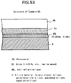
- the Si x O y N z film shown in Examples 77 and 78 was formed by the following method to form the anti-reflective layer as shown in Fig. 53.
- the film was formed by utilizing a parallel plate plasma CVD process, ECR plasma CVD process or bias ECR plasma CVD process at a microwave (2.45 GHz) from a gas mixture of SiH 4 + O 2 + N 2 or a gas mixture of SiH 4 + N 2 O using Ar as a buffer gas.
- the Si x O y N z film shown in Examples 77 and 78 was formed by the following method to form the anti-reflective layer as shown in Fig. 53.
- a film was formed by utilizing a parallel plate plasma CVD process, ECR plasma CVD process or a bias ECR plasma CVD process from a gas mixture of SiH 4 + O 2 + N 2 or a gas mixture of SiH 4 + N 2 O.
- the Si x O y N z film shown in Examples 77 and 78 was formed by the following method to form the anti-reflective layer as shown in Fig. 53.
- a film was formed by utilizing a parallel plate plasma CVD process, ECR plasma CVD process or a bias ECR plasma CVD process from a gas mixture of SiH 4 + O 2 + N 2 or a gas mixture of SiH 4 + N 2 O and using Ar as a buffer gas.
- the Si x N y film shown in Examples 77 and 78 was formed by the following method to form the anti-reflective layer as shown in Fig. 53.
- a film was formed by utilizing a parallel plate plasma CVD process, ECR plasma CVD process or a bias ECR plasma CVD process using a microwave (2.45 GHz) from a gas mixture of SiH 4 + NH 3 or a gas mixture of SiH 2 Cl 2 + NH 3 .
- the Si x N y film shown in Examples 77 and 78 was formed by the following method to form the anti-reflective layer as shown in Fig. 53.
- a film was formed by utilizing a parallel plate plasma CVD process, ECR plasma CVD process or a bias ECR plasma CVD process using a microwave (2.45 GHz) from a gas mixture of SiH 4 + O 2 or a gas mixture of SiH 2 Cl 2 + NH 3 using Ar as a buffer gas.
- the Si x N y film shown in Examples 77 and 78 was formed by the following method to form the anti-reflective layer as shown in Fig. 53.
- a film was formed by utilizing a parallel plate plasma CVD process, ECR plasma CVD process or a bias ECR plasma CVD process from a gas mixture of SiH 4 + NH 3 or a gas mixture of SiH 2 Cl 2 + NH 3 .
- the Si x N y film shown in Examples 77 and 78 was formed by the following method to form the anti-reflective layer as shown in Fig. 53.
- a film was formed by utilizing a parallel plate plasma CVD process, ECR plasma CVD process or a bias ECR plasma CVD process from a gas mixture of SiH 4 + O 2 or a gas mixture of SiH 2 Cl 2 + NH 3 using Ar as a buffer gas.
- the Si x O y N z or Si x N y film shown in Examples 77 and 78 was etched as the underlying material using the resist pattern as a mask by the following method.
- the Si x o y N z or Si x N y film was etched by a reactive etching process using a gas system of CHF 3 (50 - 100 SCCM) + O 2 (3 - 20 SCCM), under a pressure of about 2 Pa, with a power of about 100 - 1000 W and with the improved ionic property, to obtain a desired pattern by etching.
- the Si x O y N z or Si x N y film shown in Examples 77 and 78 was etched as the underlying material using the resist pattern as a mask by the following method.
- the Si x o y N z or Si x N y film was etched by a reactive etching process using a gas system of C 4 F 8 (30 - 70 SCCM) + CHF 3 (10 - 30 SCCM), under a pressure of about 2 Pa, with a power of about 100 - 1000 W and with the improved ionic property, to obtain a desired pattern by etching.
- the Si x O y N z or Si x N y film shown in Examples 77 and 78 was etched as the underlying material using the resist pattern as a mask by the following method.
- the Si x o y N z or Si x N y film was etched by a reactive etching process using a gas system of S 2 F 2 (5 - 30 SCCM), under a pressure of about 2 Pa, with a power of about 100 - 1000 W and with the improved ionic property, to obtain a desired pattern by etching.
- the condition for an anti-reflective layer used therein can be determined such that a stable resist pattern can be formed satisfactorily even if the resist pattern is fine. Further, according to the present invention, an anti-reflective layer with such a condition can be formed. Furthermore, according to the present invention, a novel anti-reflective layer can be developed to provide a method of forming a resist pattern using such an anti-reflective layer.
- a SiOxNy film is formed by using SiH 4 and N 2 O mix gas as raw gas. It is recognized that the formed film contains hydrogen.
- Fig.58 shows relationship between current ratio SiH 4 /N 2 O and n,k value of the formed film in this example.
- Fig.59 shows relationship between current ratio SiH 4 /N 2 O and atomic ratio of Si,O,N,H(atom %) of the formed film in this example.
- the formed SiOxNy film contains H, though the contain ratio changes according to current ratio SiH 4 /N 2 O. It shows the fact that SiOxNyHz film is formed.
- varioius x.y.z values of SioxNyHz film investigated from the current ratio SiH 4 /N 2 O based on Fig.58 which gives most suitable k and n value for i-line and excimer laser are shown in following table 1.
- WSi as refractry metal silicide, WSi with SiO 2 , and Al-1wt%Si as metal material are used as underlying material.
- various thickness of anti-reflective layers are formed on said underlying material using said SiH 4 /N 2 O mixed gas.
- SiOxNy;Hz is used as an anti-reflective layer for WSi for wavelength 150 to 450 nm
- x is 0.03 to 0.80
- y is 0.10 to 0.30
- z can be sero, but when hydrogen is contained, it is preferred that z is 0.20 to 0.60.
- SioxNy:Hz is used as an anti-reflective layer for AI-Si for wavelength 150 to 450 nm
- x is 0.03 to 0.70
- y is 0.05 to 0.30
- z can be sero, but when hydrogen is contained, it is preferred that z is 0.1 to 0.5.
- ordinarily used current ratio of SiH 4 /N 2 O for forming SiOxNy film is 0.2 to 2.0.
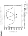
- Figs.62 and 63 show simulated anti-reflect effect ( effect for decreasing standing wave) when anti-reflective layers obtained in this example are used.
- Fig.62 shows the case that WSi with SiO 2 is used as underlying material.
- Fig.63 shows the case that AI-Si is used as underlying material.
- Fig.64 shows the measured anti-reflect effect on 0.44 m line and space pattern in real i-line lithography process. By referring Fig.64, anti-reflect effect in this example is also understood.
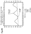
- Figs.65 and 66 show simulated anti-reflect effect.
- Fig.65 shows the case that WSi is used as underlying material (i-line, absorption ratio).
- Fig.66 shows also the case that WSi is used as underlying material (i-line, reflective ratio).
- An anti-reflective layer of 30 nm with n, k, value described in the Figures is formed, and deta are measured by using photoresist with n, k, value described in the Figures. Superior anti-reflective effect is obtained in both case of absorption ratio and reflective ratio.
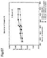
- Figs.67 and 68 show the relationship between thickness of photoresist and critical dimension. The experiment is operated using WSi as underlying material, and KrF excimer laser. Fig.67 shows the case that data are measured concerning 0.30 m line and space pattern. Fig.68 shows the case that data are measured concerning 0.35 m line and space pattern. In both cases, chemical amplifying posi resist is used.
- the material n value of which is about 2.4 and k value of which is about 0.7 is suitable as an anti-reflective layer for excimer laser on, for example, refractory metal silicide.
- SiOx, SINx, or SiOxNy is effective such an anti-reflecive layer as described above. It is considered that SiOx, SiNx, or SiOxNy with the n value and k value as described above which is effective for anti-reflectivity can be formed by controlling the n value and k value by controlling the element ratio x and y. It is , however, difficult to obtain a film with desired n value and k value by controlling the ratio by suitable means.
- the anti-reflective layer is formed by using as raw gas containing at least silicon element and oxide element.
- the element ratio x of SiOx by using gas current ratio as parameter, it is possible to make x smaller through using higher ratio of raw gas containing silicon element.
- the atomic ratio can be controlled, and the optical constant (n,k) can be controlled.
- SiH 4 is used as raw gas containing at least silicon element
- N 2 O is used as raw gas containing at least oxide element.
- the film with desired anti-reflective effect can be formed by controlling the optical constant through using current ratio of SiH 4 and N 2 O as parameter.
- Fig.58 shows the change of the optical constant of the formed film when the current ratio of SiH 4 and N 2 O in parallel electrodetype plasuma CVD camber is changed.
- the suitable example of film forming conditions for excimer lithography are as follows.
- an anti-reflective layer is formed by using at least one kind of organic compounds containing at least silicon element as raw material.
- coverage of an anti-reflective layer on step improves. Namely, a difference between thickness of an anti-reflective layer on even portion and that of perpendicular portion of step in this example is small, and uniformity of anti-reflective effect in semiconductor device tip improves.
- this example can be said it is especally effective for device with severe unevenness.
- used conditions for forming film in parallel electrode plasuma CVD chamber are as follows.
- SiH 4 which is Si source gas without containing O, N
- the example of conditions for forming film in parallel electrode plasuma CVD chamber are as follows.
Landscapes
- Physics & Mathematics (AREA)
- General Physics & Mathematics (AREA)
- Engineering & Computer Science (AREA)
- Architecture (AREA)
- Structural Engineering (AREA)
- Exposure Of Semiconductors, Excluding Electron Or Ion Beam Exposure (AREA)
- Liquid Crystal (AREA)
- Led Devices (AREA)
- Photosensitive Polymer And Photoresist Processing (AREA)
- Exposure And Positioning Against Photoresist Photosensitive Materials (AREA)
Applications Claiming Priority (7)
| Application Number | Priority Date | Filing Date | Title |
|---|---|---|---|
| JP24431492 | 1992-08-20 | ||
| JP24431492 | 1992-08-20 | ||
| JP31607392 | 1992-10-31 | ||
| JP31607392 | 1992-10-31 | ||
| JP4359750A JP2897569B2 (ja) | 1991-12-30 | 1992-12-29 | レジストパターン形成時に用いる反射防止膜の条件決定方法と、レジストパターン形成方法 |
| JP35975092 | 1992-12-29 | ||
| EP93113219A EP0588087B1 (de) | 1992-08-20 | 1993-08-18 | Verfahren zur Bildung eines Lackmusters unter Verwendung einer optimierten Antireflexionsschicht. |
Related Parent Applications (1)
| Application Number | Title | Priority Date | Filing Date |
|---|---|---|---|
| EP93113219A Division EP0588087B1 (de) | 1992-08-20 | 1993-08-18 | Verfahren zur Bildung eines Lackmusters unter Verwendung einer optimierten Antireflexionsschicht. |
Publications (2)
| Publication Number | Publication Date |
|---|---|
| EP0933683A2 true EP0933683A2 (de) | 1999-08-04 |
| EP0933683A3 EP0933683A3 (de) | 1999-12-15 |
Family
ID=27333224
Family Applications (2)
| Application Number | Title | Priority Date | Filing Date |
|---|---|---|---|
| EP93113219A Expired - Lifetime EP0588087B1 (de) | 1992-08-20 | 1993-08-18 | Verfahren zur Bildung eines Lackmusters unter Verwendung einer optimierten Antireflexionsschicht. |
| EP99108501A Withdrawn EP0933683A3 (de) | 1992-08-20 | 1993-08-18 | Verfahren zur Bildung eines Lackmusters unter Verwendung einer, aus Siliziumkarbid, optimierten Antireflexionsschicht |
Family Applications Before (1)
| Application Number | Title | Priority Date | Filing Date |
|---|---|---|---|
| EP93113219A Expired - Lifetime EP0588087B1 (de) | 1992-08-20 | 1993-08-18 | Verfahren zur Bildung eines Lackmusters unter Verwendung einer optimierten Antireflexionsschicht. |
Country Status (3)
| Country | Link |
|---|---|
| EP (2) | EP0588087B1 (de) |
| DE (1) | DE69326982T2 (de) |
| TW (2) | TW363146B (de) |
Families Citing this family (22)
| Publication number | Priority date | Publication date | Assignee | Title |
|---|---|---|---|---|
| US5378659A (en) * | 1993-07-06 | 1995-01-03 | Motorola Inc. | Method and structure for forming an integrated circuit pattern on a semiconductor substrate |
| JPH08255907A (ja) * | 1995-01-18 | 1996-10-01 | Canon Inc | 絶縁ゲート型トランジスタ及びその製造方法 |
| TW388083B (en) * | 1995-02-20 | 2000-04-21 | Hitachi Ltd | Resist pattern-forming method using anti-reflective layer, resist pattern formed, and method of etching using resist pattern and product formed |
| US5918147A (en) * | 1995-03-29 | 1999-06-29 | Motorola, Inc. | Process for forming a semiconductor device with an antireflective layer |
| US5968324A (en) | 1995-12-05 | 1999-10-19 | Applied Materials, Inc. | Method and apparatus for depositing antireflective coating |
| FR2749973B1 (fr) | 1996-06-13 | 1998-09-25 | France Telecom | Procede de gravure de la grille en technologie mos utilisant un masque dur a base de sion |
| US6127262A (en) * | 1996-06-28 | 2000-10-03 | Applied Materials, Inc. | Method and apparatus for depositing an etch stop layer |
| US6083852A (en) | 1997-05-07 | 2000-07-04 | Applied Materials, Inc. | Method for applying films using reduced deposition rates |
| US6156149A (en) * | 1997-05-07 | 2000-12-05 | Applied Materials, Inc. | In situ deposition of a dielectric oxide layer and anti-reflective coating |
| US6562544B1 (en) * | 1996-11-04 | 2003-05-13 | Applied Materials, Inc. | Method and apparatus for improving accuracy in photolithographic processing of substrates |
| US6274292B1 (en) | 1998-02-25 | 2001-08-14 | Micron Technology, Inc. | Semiconductor processing methods |
| US6174810B1 (en) | 1998-04-06 | 2001-01-16 | Motorola, Inc. | Copper interconnect structure and method of formation |
| US6281100B1 (en) | 1998-09-03 | 2001-08-28 | Micron Technology, Inc. | Semiconductor processing methods |
| US6268282B1 (en) | 1998-09-03 | 2001-07-31 | Micron Technology, Inc. | Semiconductor processing methods of forming and utilizing antireflective material layers, and methods of forming transistor gate stacks |
| JP2002530885A (ja) * | 1998-11-25 | 2002-09-17 | アドバンスト・マイクロ・ディバイシズ・インコーポレイテッド | 半導体製造における金属形状のパターニングのためのシランベース酸化物反射防止膜 |
| US6828683B2 (en) | 1998-12-23 | 2004-12-07 | Micron Technology, Inc. | Semiconductor devices, and semiconductor processing methods |
| US7235499B1 (en) | 1999-01-20 | 2007-06-26 | Micron Technology, Inc. | Semiconductor processing methods |
| US7067414B1 (en) | 1999-09-01 | 2006-06-27 | Micron Technology, Inc. | Low k interlevel dielectric layer fabrication methods |
| US6440860B1 (en) | 2000-01-18 | 2002-08-27 | Micron Technology, Inc. | Semiconductor processing methods of transferring patterns from patterned photoresists to materials, and structures comprising silicon nitride |
| US6605394B2 (en) * | 2001-05-03 | 2003-08-12 | Applied Materials, Inc. | Organic bottom antireflective coating for high performance mask making using optical imaging |
| US6703169B2 (en) | 2001-07-23 | 2004-03-09 | Applied Materials, Inc. | Method of preparing optically imaged high performance photomasks |
| FR2985255B1 (fr) * | 2011-12-28 | 2015-08-07 | Ecole Polytech | Article revetu d'un revetement interferentiel ayant des proprietes stables dans le temps. |
Family Cites Families (9)
| Publication number | Priority date | Publication date | Assignee | Title |
|---|---|---|---|---|
| FR1534173A (fr) * | 1966-08-10 | 1968-07-26 | Gen Precision Inc | Procédé pour former des réserves photographiques sur des supports transparents outranslucides avec une résolution élevée |
| JPS596540A (ja) * | 1982-07-05 | 1984-01-13 | Toshiba Corp | 半導体装置の製造方法 |
| US4451969A (en) * | 1983-01-10 | 1984-06-05 | Mobil Solar Energy Corporation | Method of fabricating solar cells |
| JPH0255416A (ja) * | 1988-08-19 | 1990-02-23 | Seiko Epson Corp | 半導体装置 |
| EP0379604B1 (de) * | 1989-01-23 | 1995-05-31 | Siemens Aktiengesellschaft | Verfahren zum Herstellen einer Siliziumnitridschicht, wie sie als Antireflexschicht in Photolithographieprozessen bei der Herstellung hochintegrierter Halbleiterschaltungen verwendet wird |
| JPH0712016B2 (ja) * | 1989-12-26 | 1995-02-08 | 信越化学工業株式会社 | X線リソグラフィー用SiC膜の成膜方法 |
| JP2895894B2 (ja) * | 1989-12-27 | 1999-05-24 | 三洋電機株式会社 | 固体撮像素子の製造方法 |
| JPH0456769A (ja) * | 1990-06-22 | 1992-02-24 | Nippon Steel Corp | 微結晶を含有する非晶質炭化ケイ素膜の形成方法 |
| JP2791525B2 (ja) * | 1992-04-16 | 1998-08-27 | 三菱電機株式会社 | 反射防止膜の選定方法およびその方法により選定された反射防止膜 |
-
1993
- 1993-08-10 TW TW082106366A patent/TW363146B/zh not_active IP Right Cessation
- 1993-08-10 TW TW086108534A patent/TW349185B/zh not_active IP Right Cessation
- 1993-08-18 DE DE69326982T patent/DE69326982T2/de not_active Expired - Lifetime
- 1993-08-18 EP EP93113219A patent/EP0588087B1/de not_active Expired - Lifetime
- 1993-08-18 EP EP99108501A patent/EP0933683A3/de not_active Withdrawn
Also Published As
| Publication number | Publication date |
|---|---|
| TW349185B (en) | 1999-01-01 |
| TW363146B (en) | 1999-07-01 |
| EP0588087A3 (de) | 1995-08-02 |
| EP0933683A3 (de) | 1999-12-15 |
| DE69326982D1 (de) | 1999-12-16 |
| DE69326982T2 (de) | 2000-04-20 |
| EP0588087A2 (de) | 1994-03-23 |
| EP0588087B1 (de) | 1999-11-10 |
Similar Documents
| Publication | Publication Date | Title |
|---|---|---|
| US5472827A (en) | Method of forming a resist pattern using an anti-reflective layer | |
| EP0588087B1 (de) | Verfahren zur Bildung eines Lackmusters unter Verwendung einer optimierten Antireflexionsschicht. | |
| US5472829A (en) | Method of forming a resist pattern by using an anti-reflective layer | |
| US5710067A (en) | Silicon oxime film | |
| US6514667B2 (en) | Tunable vapor deposited materials as antireflective coatings, hardmasks and as combined antireflective coating/hardmasks and methods of fabrication thereof and applications thereof | |
| US5998100A (en) | Fabrication process using a multi-layer antireflective layer | |
| KR100188508B1 (ko) | 비정질탄소막을 사용하는 패턴형성방법과 에칭방법 및 비정질탄소막 형성방법 | |
| JP4420592B2 (ja) | 半導体素子の微細パターン形成方法 | |
| US6884734B2 (en) | Vapor phase etch trim structure with top etch blocking layer | |
| US5677111A (en) | Process for production of micropattern utilizing antireflection film | |
| US8293460B2 (en) | Double exposure patterning with carbonaceous hardmask | |
| US20040092089A1 (en) | Polysilicon processing using an anti-reflective dual layer hardmask for 193 nm lithography | |
| US6365320B1 (en) | Process for forming anti-reflective film for semiconductor fabrication using extremely short wavelength deep ultraviolet photolithography | |
| US6395644B1 (en) | Process for fabricating a semiconductor device using a silicon-rich silicon nitride ARC | |
| US5342481A (en) | Dry etching method | |
| US6479401B1 (en) | Method of forming a dual-layer anti-reflective coating | |
| JP2897569B2 (ja) | レジストパターン形成時に用いる反射防止膜の条件決定方法と、レジストパターン形成方法 | |
| US6620575B2 (en) | Construction of built-up structures on the surface of patterned masking used for polysilicon etch | |
| JPH06342744A (ja) | a−Cによる反射防止 | |
| KR20030040030A (ko) | 반도체소자 제조방법 | |
| JPH0851072A (ja) | レジストパターン形成方法および反射防止膜形成方法 | |
| JP2953348B2 (ja) | レジストパターン形成方法、反射防止膜形成方法、反射防止膜および半導体装置 | |
| KR20040057502A (ko) | 불화아르곤 노광원을 이용한 반도체소자의 패턴 형성 방법 | |
| JPH0855790A (ja) | レジストパターン形成方法および反射防止膜形成方法 | |
| US20070119813A1 (en) | Gate patterning method for semiconductor processing |
Legal Events
| Date | Code | Title | Description |
|---|---|---|---|
| PUAI | Public reference made under article 153(3) epc to a published international application that has entered the european phase |
Free format text: ORIGINAL CODE: 0009012 |
|
| 17P | Request for examination filed |
Effective date: 19990430 |
|
| AC | Divisional application: reference to earlier application |
Ref document number: 588087 Country of ref document: EP |
|
| AK | Designated contracting states |
Kind code of ref document: A2 Designated state(s): DE FR NL |
|
| PUAL | Search report despatched |
Free format text: ORIGINAL CODE: 0009013 |
|
| RIC1 | Information provided on ipc code assigned before grant |
Free format text: 6G 03F 7/09 A, 6H 01L 21/027 B, 6H 01L 21/3213 B, 6C 23C 16/32 B, 6C 23C 14/06 B, 6H 01L 21/314 B, 6C 23C 16/30 B, 6C 23C 16/40 B |
|
| AK | Designated contracting states |
Kind code of ref document: A3 Designated state(s): DE FR NL |
|
| 17Q | First examination report despatched |
Effective date: 20010910 |
|
| STAA | Information on the status of an ep patent application or granted ep patent |
Free format text: STATUS: THE APPLICATION IS DEEMED TO BE WITHDRAWN |
|
| 18D | Application deemed to be withdrawn |
Effective date: 20020122 |