EP0933809B1 - Procédé de montage de dispositifs semiconducteurs du type flip-chip - Google Patents
Procédé de montage de dispositifs semiconducteurs du type flip-chip Download PDFInfo
- Publication number
- EP0933809B1 EP0933809B1 EP99300697A EP99300697A EP0933809B1 EP 0933809 B1 EP0933809 B1 EP 0933809B1 EP 99300697 A EP99300697 A EP 99300697A EP 99300697 A EP99300697 A EP 99300697A EP 0933809 B1 EP0933809 B1 EP 0933809B1
- Authority
- EP
- European Patent Office
- Prior art keywords
- resin composition
- substrate
- semiconductor chip
- particle size
- weight
- Prior art date
- Legal status (The legal status is an assumption and is not a legal conclusion. Google has not performed a legal analysis and makes no representation as to the accuracy of the status listed.)
- Expired - Lifetime
Links
Images

Classifications
-
- H—ELECTRICITY
- H10—SEMICONDUCTOR DEVICES; ELECTRIC SOLID-STATE DEVICES NOT OTHERWISE PROVIDED FOR
- H10W—GENERIC PACKAGES, INTERCONNECTIONS, CONNECTORS OR OTHER CONSTRUCTIONAL DETAILS OF DEVICES COVERED BY CLASS H10
- H10W74/00—Encapsulations, e.g. protective coatings
- H10W74/01—Manufacture or treatment
- H10W74/012—Manufacture or treatment of encapsulations on active surfaces of flip-chip devices, e.g. forming underfills
-
- H—ELECTRICITY
- H10—SEMICONDUCTOR DEVICES; ELECTRIC SOLID-STATE DEVICES NOT OTHERWISE PROVIDED FOR
- H10W—GENERIC PACKAGES, INTERCONNECTIONS, CONNECTORS OR OTHER CONSTRUCTIONAL DETAILS OF DEVICES COVERED BY CLASS H10
- H10W72/00—Interconnections or connectors in packages
- H10W72/30—Die-attach connectors
-
- H—ELECTRICITY
- H10—SEMICONDUCTOR DEVICES; ELECTRIC SOLID-STATE DEVICES NOT OTHERWISE PROVIDED FOR
- H10W—GENERIC PACKAGES, INTERCONNECTIONS, CONNECTORS OR OTHER CONSTRUCTIONAL DETAILS OF DEVICES COVERED BY CLASS H10
- H10W74/00—Encapsulations, e.g. protective coatings
- H10W74/10—Encapsulations, e.g. protective coatings characterised by their shape or disposition
- H10W74/15—Encapsulations, e.g. protective coatings characterised by their shape or disposition on active surfaces of flip-chip devices, e.g. underfills
-
- H—ELECTRICITY
- H10—SEMICONDUCTOR DEVICES; ELECTRIC SOLID-STATE DEVICES NOT OTHERWISE PROVIDED FOR
- H10W—GENERIC PACKAGES, INTERCONNECTIONS, CONNECTORS OR OTHER CONSTRUCTIONAL DETAILS OF DEVICES COVERED BY CLASS H10
- H10W72/00—Interconnections or connectors in packages
- H10W72/071—Connecting or disconnecting
- H10W72/072—Connecting or disconnecting of bump connectors
-
- H—ELECTRICITY
- H10—SEMICONDUCTOR DEVICES; ELECTRIC SOLID-STATE DEVICES NOT OTHERWISE PROVIDED FOR
- H10W—GENERIC PACKAGES, INTERCONNECTIONS, CONNECTORS OR OTHER CONSTRUCTIONAL DETAILS OF DEVICES COVERED BY CLASS H10
- H10W72/00—Interconnections or connectors in packages
- H10W72/071—Connecting or disconnecting
- H10W72/073—Connecting or disconnecting of die-attach connectors
-
- H—ELECTRICITY
- H10—SEMICONDUCTOR DEVICES; ELECTRIC SOLID-STATE DEVICES NOT OTHERWISE PROVIDED FOR
- H10W—GENERIC PACKAGES, INTERCONNECTIONS, CONNECTORS OR OTHER CONSTRUCTIONAL DETAILS OF DEVICES COVERED BY CLASS H10
- H10W72/00—Interconnections or connectors in packages
- H10W72/50—Bond wires
- H10W72/551—Materials of bond wires
- H10W72/552—Materials of bond wires comprising metals or metalloids, e.g. silver
- H10W72/5522—Materials of bond wires comprising metals or metalloids, e.g. silver comprising gold [Au]
-
- H—ELECTRICITY
- H10—SEMICONDUCTOR DEVICES; ELECTRIC SOLID-STATE DEVICES NOT OTHERWISE PROVIDED FOR
- H10W—GENERIC PACKAGES, INTERCONNECTIONS, CONNECTORS OR OTHER CONSTRUCTIONAL DETAILS OF DEVICES COVERED BY CLASS H10
- H10W72/00—Interconnections or connectors in packages
- H10W72/851—Dispositions of multiple connectors or interconnections
- H10W72/853—On the same surface
- H10W72/856—Bump connectors and die-attach connectors
-
- H—ELECTRICITY
- H10—SEMICONDUCTOR DEVICES; ELECTRIC SOLID-STATE DEVICES NOT OTHERWISE PROVIDED FOR
- H10W—GENERIC PACKAGES, INTERCONNECTIONS, CONNECTORS OR OTHER CONSTRUCTIONAL DETAILS OF DEVICES COVERED BY CLASS H10
- H10W90/00—Package configurations
- H10W90/701—Package configurations characterised by the relative positions of pads or connectors relative to package parts
- H10W90/721—Package configurations characterised by the relative positions of pads or connectors relative to package parts of bump connectors
- H10W90/724—Package configurations characterised by the relative positions of pads or connectors relative to package parts of bump connectors between a chip and a stacked insulating package substrate, interposer or RDL
Definitions
- This invention relates to a method for fabricating semiconductor devices of the flip chip design.
- the conventional system of connecting semiconductor chips to lead frames using gold wires is employed less frequently.
- the flip chip system of mounting semiconductor chips to substrates or boards via solder is more frequently employed in the recent years, as in the prior art EP-A-0 446 580.
- the reliability of semiconductor chips is improved by infiltrating a liquid epoxy resin into the space between semiconductor chips and substrates and curing the resin therein. Since the space between semiconductor chips and substrates is filled with the resin by capillary action, the filling step requires a very long time.
- the inorganic filler in the encapsulating resin composition can settle during heat curing, resulting in a difference in expansion coefficient between upper and lower portions of the cured resin. This detracts from the reliability of semiconductor devices.
- the space between a semiconductor chip and a substrate can be rapidly sealed with a resin encapsulant by transfer molding, more particularly by introducing a specific encapsulating resin composition in molten state and under pressure into the space between the chip and the substrate and heat curing the resin thereat. Then encapsulation can be completed within a very short cycle without allowing the filler to settle.
- Semiconductor devices are manufactured to high reliability.
- the present invention provides a method for fabricating (or manufacturing) a semiconductor device, comprising the steps of placing a semiconductor chip having contacts over a circuit substrate having interconnecting electrodes such that the semiconductor chip contacts abut against the substrate electrodes via solder bumps; heating and fusing the solder bumps to join the semiconductor chip to the substrate; placing the substrate having the semiconductor chip mounted thereon in a cavity of a mold; melting a resin composition to produce an encapsulating resin composition in molten state; feeding said molten composition; under pressure into the mold cavity through a gate for forcibly filling the space between said substrate and said semiconductor chip with the resin composition; and heat-curing the resin composition at a molding temperature in the range 130-200°C for encapsulating the space with the resin composition.
- the encapsulating resin composition comprises (a) an epoxy resin, (b) a phenolic resin curing agent, and (c) a particulate inorganic filler having a maximum particle size of up to 24 ⁇ m as essential components.
- the content of filler (c) is 50 to 85% by weight based on the entire composition.
- the composition has a melt viscosity of 5 to 200 poises at the molding temperature.
- a substrate 1 has a wiring circuit formed on one surface thereof, which is depicted as interconnecting electrodes 2.
- a semiconductor chip 4 having contacts 5 is placed over the substrate 1 such that the semiconductor chip contacts 5 abut against the substrate electrodes 2 via solder bumps 3.
- the solder bumps 3 are then heated and fused to join the semiconductor chip 4 to the substrate 1.
- the distance between the semiconductor chip and the substrate is about 10 ⁇ m to about 150 ⁇ m, and desirably about 20 ⁇ m to about 100 ⁇ m.
- the chip-to-substrate distance is desirably 30 ⁇ m or more.
- the solder bumps 3 are distributed in a pattern as shown in FIG. 2.
- the substrate having the semiconductor chip mounted thereon is then set in a cavity of a mold.
- An encapsulating resin composition in molten state and under pressure is introduced into the mold cavity through a gate of the mold for forcibly filling the space between the substrate and the semiconductor chip with the resin composition, and cured thereat. This is a so-called transfer molding process. In this way, the space between the substrate and the semiconductor chip is encapsulated with the resin composition.
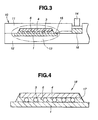
- a mold 10 includes an upper mold section 11 and a lower mold section 12 defining a cavity 13 which are removably mated.
- the substrate 1 having the semiconductor chip 4 mounted thereon is set in the cavity 13 of the lower mold section 12 whereupon the upper mold section 11 is moved back to close the cavity 13.
- the mold is heated at a suitable temperature, preferably about 130 to about 200°C. If the mold temperature is below 130°C, the encapsulating resin composition would have a higher melt viscosity so that the resin can sweep away solder bumps during molding or allow voids to be left in the interior. If the mold temperature is above 200°C, rapid reaction can result in short-filling.
- the encapsulating resin composition 16 is admitted in a plunger pot and compressed under a plunger 14. Before admitting into the plunger pot, the encapsulating resin composition may have a cylindrical preform or be in granular form.
- a pressure below 10 kgf/cm 2 would be too low to achieve full filling whereas a pressure above 100 kgf/cm 2 would carry away the solder. It is preferred from the reliability standpoint to set the pressure as high as possible within the range causing no troubles.
- the molten resin composition 16 is introduced under pressure into the cavity 13 through a gate 15 of the mold 10 for forcibly filling the space 6 between the substrate 1 and the semiconductor chip 4 with the resin composition.
- the resin composition is cured in the space 6, yielding a semiconductor device 18 having the space 6 sealed with the resin 17 as shown in FIG. 4.
- the curing time is usually 60 to 240 seconds, desirably 60 to 120 seconds.
- 3P system the pre-packaged-process
- the encapsulating resin composition used herein is a curable epoxy resin composition comprising (a) an epoxy resin, (b) a phenolic resin curing agent, and (c) an inorganic filler as essential components. Since semiconductor chips typically dimensioned 5 to 20 mm by 5 to 20 mm by 0.1 to 0.6 mm thick and presenting a space of 10 to 150 ⁇ m must be encapsulated, the resin composition used herein should have different flow properties and cure properties than the conventional well-known semiconductor device-encapsulating resin compositions. In particular, the viscosity of the composition during molding is crucial. Specifically, the composition should have a melt viscosity of 5 to 200 poises at the molding temperature.
- the composition has a melt viscosity of 5 to 200 poises, desirably 5 to 100 poises, more desirably 10 to 50 poises, as measured at the molding temperature. Since it is desirable to finish the resin injection within about 3 to 30 seconds, the resin composition should desirably have a gel time of at least 20 seconds, more desirably at least 30 seconds, most desirably at least 35 seconds, at the molding temperature. As a measure of fluidity, the resin composition should desirably have a spiral flow of about 100 to 250 cm, more desirably about 150 to 250 cm as measured at 175°C and 70 kgf/cm 2 .
- Component (a) is any of conventional well-known epoxy resins having at least two epoxy groups per molecule.
- Exemplary are bisphenol type epoxy resins such as bisphenol A and bisphenol F type epoxy resins, novolak type epoxy resins such as phenol novolak and cresol novolak type epoxy resins, cyclopentadiene epoxy resins, triphenol alkane epoxy resins such as triphenol methane epoxy resins and triphenol propane epoxy resins, biphenyl epoxy resins, naphthalene ring-containing epoxy resins, phenol aralkyl epoxy resins, and biphenyl aralkyl epoxy resins. Also useful are epoxy resins of the following structural formulae.
- G is glycidyl
- Me is methyl
- n is an integer of 0 to 10, preferably 0 to 3.
- the epoxy resins should desirably have a total chlorine content of up to about 1,500 ppm, more desirably up to about 1,000 ppm.
- the water-extracted chlorine content is preferably up to about 5 ppm.
- a total chlorine content in excess of about 1,500 ppm or a water-extracted chlorine content of more than about 5 ppm can be detrimental to the moisture-resistant reliability of semiconductors.
- the curing agent (b) of the resin composition according to the invention is usually selected from among conventional phenolic resin curing agents known to cause epoxy resins to cure.
- the use of phenolic resins is required from the reliability standpoint. Any phenolic resin having at least two phenolic hydroxyl groups in a molecule may be used.
- Exemplary phenolic resins include bisphenol resins such as bisphenol A resins and bisphenol F resins, novolak resins such as phenol novolak resins and cresol novolak resins, phenol aralkyl resins, naphthalene ring-containing phenolic resins, cyclopentadiene phenolic resins, triphenol alkane resins such as triphenol methane resins and triphenol propane resins, biphenyl resins, and biphenyl aralkyl resins as well as phenolic hydroxy group-bearing resins of the following structures.
- Letter n is an integer of 0 to 10, preferably 0 to 3.
- the concentrations of extracted ions such as chloride ions and sodium ions are preferably each up to about 10 ppm, and more preferably up to about 5 ppm.
- the mixing ratio of the epoxy resin and the phenolic resin is preferably such that about 0.5 to 1.6 mol, more preferably about 0.6 to 1.4 mol of phenolic hydroxyl groups in the phenolic resins are available per mol of epoxy groups in the epoxy resins. Less than 0.5 mol of phenolic hydroxyl groups on this basis would allow homo-polymerization of more epoxy groups due to shortage of hydroxyl groups, leading to a lower glass transition temperature. On the other than, a mixing ratio in excess of 1.6 mol of phenolic hydroxyl groups would result in a lower crosslinking density and lower strength due to lower reactivity.
- phosphorus compounds, imidazole derivatives and cycloamidine derivatives may be used as a curing promoter.
- the curing promoter is blended in an amount of 0 to about 10 parts, preferably about 0.01 to 10 parts by weight per 100 parts by weight of the epoxy resin and the phenolic resin combined.
- Component (c) is an inorganic filler having a maximum particle size of up to 24 ⁇ m.
- Useful fillers include fused silica ground in ball mills, spherical silica prepared by flame fusion, spherical silica prepared by the sol-gel process, crystalline silica, alumina, boron nitride, aluminum nitride, silicon nitride, magnesia, and magnesium silicate.
- fillers having a greater heat conductivity and a lower coefficient of expansion such as alumina, boron nitride, aluminum nitride and silicon nitride. They may also be blended with fused silica.
- spherical inorganic fillers typically fused silica, are often used, and alumina and aluminum nitride are preferred when heat conductivity is required.
- the amount of fused silica or alumina used is preferably 100 to 550 parts, more preferably 200 to 450 parts by weight per 100 parts by weight of the epoxy resin and the curing agent combined. Less than 100 parts of fused silica or alumina would be too small to fully reduce the coefficient of expansion whereas compositions containing more than 550 parts of fused silica or alumina would become too viscous to mold.
- the inorganic filler used herein typically fused silica or alumina, has such a particle size distribution that the mean particle size is from 1 to 15 ⁇ m, more desirably 2 to 10 ⁇ m, fine particles having a particle size of up to 5 ⁇ m account for 20 to 60% by weight of the entire filler, the maximum particle size is up to 24 ⁇ m, more desirably up to 20 ⁇ m, most desirably up to 10 ⁇ m, and the specific surface area (BET adsorption method) is 3.5 to 6.0 m 2 /g, more desirably 4.0 to 5.0 m 2 /g.
- the mean particle size is from 1 to 15 ⁇ m, more desirably 2 to 10 ⁇ m
- fine particles having a particle size of up to 5 ⁇ m account for 20 to 60% by weight of the entire filler
- the maximum particle size is up to 24 ⁇ m, more desirably up to 20 ⁇ m, most desirably up to 10 ⁇ m
- fine particles having a particle size of up to 5 ⁇ m constitute less than 20% by weight of the entire filler, the space between the semiconductor chip and the substrate would not be fully filled, giving rise to the problems of voids and solder bump failure. If fine particles having a particle size of up to 5 ⁇ m constitute more than 60% by weight of the entire filler, which means a greater proportion of fines, the wetting of the filler surface with the resin becomes insufficient and the composition becomes increased in viscosity, which requires to increase the molding pressure, sometimes causing solder bump failure. More desirable results are obtained when fine particles having a particle size of up to 5 ⁇ m account for 30 to 50% by weight of the entire filler.
- the maximum particle size of the filler is up to 1/5, preferably up to 1/10 of the distance between the substrate and the semiconductor chip.
- the mean particle size can be determined as a weight average value (or median diameter) by means of a particle size distribution meter of the laser light diffraction system, for example.
- an auxiliary silica filler ranging from a silica filler having a particle size of 3 ⁇ m to ultra-microparticulate silica (particle size of up to 0.05 ⁇ m, preferably 0.001 to 0.05 ⁇ m) may be added to the above-described filler for assisting in closest packing of the filler and imparting thixotropy.
- ultra-microparticulate silica having a specific surface area of 50 to 300 m 2 /g or a particle size of 0.001 to 0.05 ⁇ m as typified by aerosil, a fine silica filler having a particle size of 0.05 to 0.5 ⁇ m, and a silica filler having a particle size of 0.5 to 3 ⁇ m in a suitable proportion.
- compositions consist of 0 to 5% by weight of ultra-microparticulate silica, 1 to 15% by weight of silica having a particle size of 0.05 to 0.5 ⁇ m, and 5 to 20% by weight of silica having a particle size of 0.5 to 3 ⁇ m, based on the weight of the entire filler.
- the mixture may be prepared and blended so that it has a mean particle size of 1 ⁇ m or less.
- the inorganic filler is contained in an amount of 50 to 85%, especially 70 to 82% by weight based on the entire composition.
- Compositions with a filler content of less than 50% by weight have a low viscosity, but a high coefficient of expansion so that the encapsulant may peel from the semiconductor chip surface in a thermal cycling test.
- Compositions with a filler content of more than 85% by weight have a too high viscosity and become less effective in filling capability, causing short-filling defects.
- the epoxy resin composition according to the invention may contain a well-known stress-reducing agent.
- stress-reducing agents include silicone rubber powder, silicone gel powder, silicone-modified epoxy resins, silicone-modified phenolic resins, and thermoplastic resins of methyl methacrylate/butadiene/styrene and derivatives thereof including their hydrogenated products.
- any of well-known diluents may be added.
- diluents include n-butylglycidyl ether, phenylglycidyl ether, styrene oxide, t-butylphenylglycidyl ether, dicyclopentadiene diepoxide, phenol, cresol, and t-butylphenol.
- additives which can be added to the epoxy resin composition of the invention include flame retardants such as brominated epoxy resins and antimony trioxide; coupling agents such as silane coupling agents, titanium coupling agents, and aluminum coupling agents; coloring agents such as carbon black; wetting modifiers and antifoaming agents such as nonionic surfactants, fluorochemical surfactants, and silicone oil.
- composition of the invention can be prepared by uniformly mixing the above-mentioned essential and optional components in a high-speed mixer or the like and then thoroughly milling in a twin-roll mill or continuous kneader.
- Each resin composition was prepared by mixing the ingredients shown in Table 1 in the proportion shown in Table 1. The ingredients were mixed in a high-speed mixture for 10 minutes, milled in a continuous kneader at 50 to 100°C, and sheeted. The sheet was cooled, ground, and compacted into cylindrical tablets.
- Epoxy resin (1) epoxy equivalent 165
- Epoxy resin (2) epoxy equivalent 210
- n is a number to give an epoxy equivalent of 210.
- Epoxy resin (3) epoxy equivalent 195
- Phenolic resin (1) novolak type phenolic resin, hydroxyl equivalent 110 Phenolic resin (2): phenol aralkyl resin MEH7800 (Meiwa Chemicals K.K.), hydroxyl equivalent 175 Brominated epoxy resin: BREN-S (Nippon Kayaku K.K.), epoxy equivalent 280
- Phenolic resin (2) phenol aralkyl resin MEH7800 (Meiwa Chemicals K.K.), hydroxyl equivalent 175
- Brominated epoxy resin BREN-S (Nippon Kayaku K.K.)
- epoxy equivalent 280 Inorganic fillers: The mean particle size and the maximum particle size were measured by using a laser diffraction type particle size distribution measuring apparatus: Granurometer 920 manufactured by CILAS ALCATEL CO., LTD. in France.
- Spiral flow was measured by transfer molding a composition at a temperature of 175°C and a pressure of 70 kgf/cm 2 .
- the melt viscosity was measured at a temperature of 175°C under a load of 10 kg using a constant-load, orifice-type flow testing apparatus of the kind known in Japan as a Koka-type flow tester (Shimazu Mfg. K.K.) equipped with a nozzle having a diameter of 1 mm.
- Test specimens with dimensions of 4x4x15 mm were obtained by molding each composition at 175°C and 70 kgf/cm 2 for a time of 2 minutes and post-curing at 180°C for 4 hours. Measurement of both properties was carried out by raising the temperature of the test specimen at a rate of 5°C/min in a dilatometer.
- a semiconductor device assembly as used above was encapsulated using a conventional flip-chip underfill material (epoxy resin composition) of the acid anhydride curing type (Comparative Example 3).
- the flip-chip underfill material of the acid anhydride curing type was of the following composition. Parts by weight Bisphenol A type epoxy resin 50 4-methylhexahydrophthalic anhydride 30 Spherical silica (mean particle size 5 ⁇ m, maximum particle size 15 ⁇ m) 100 2-phenylimidazole 0.2
- Example 1 Five samples for each of the semiconductor device encapsulated in Example 1 and the semiconductor device encapsulated in Comparative Example 3 were placed in a pressure cooker at 121°C and 2.1 atmospheres. The samples were taken out at predetermined time intervals, and the separation between the chip surface and the resin was observed by an ultrasonic flaw detector. The results are shown in Table 4. Table 4 Number of defective samples/total Time 48 hr. 96 hr. 196 hr. 392 hr. Example 1 0/5 0/5 0/5 0/5 Comparative Example 3 0/5 0/5 1/5 3/5
Landscapes
- Structures Or Materials For Encapsulating Or Coating Semiconductor Devices Or Solid State Devices (AREA)
- Compositions Of Macromolecular Compounds (AREA)
Claims (7)
- Procédé pour fabriquer un dispositif à semi-conducteur (18) comprenant les étapes consistant à, dans l'ordre suivant:placer une puce à semi-conducteur (4) ayant des contacts (5) sur un substrat de circuit (1) ayant des électrodes d'interconnexion (2), telles que les contacts de la puce à semi-conducteur (5) viennent en butée contre les électrodes du substrat (2) via des perles de soudure (3);chauffer et fondre les perles de soudure (3) pour joindre la puce à semi-conducteur (4) au substrat (1);placer le substrat (1) où la puce à semi-conducteur (4) est montée dans la cavité d'un moule (10);faire fondre une composition de résine (16) pour produire une composition de résine encapsulante dans un état fondu;amener ladite composition de résine fondue (16) sous pression à l'intérieur de la cavité du moule à travers une porte (15) pour remplir en force l'espace (6) entre ledit substrat (1) et ladite puce à semi-conducteur (4) avec la composition de résine (16), le moule étant à une température de moulage comprise entre 130 et 200 °C, etpolymériser à chaud la composition de résine pour encapsuler l'espace (6) avec la composition de résine (17);ladite composition de résine comprenant (a) une résine époxy, (b) un agent de polymérisation de résine phénolique, et (c) de 50 à 85 % en masse, en se basant sur la composition d'ensemble d'un matériau de remplissage inorganique particulaire ayant une taille de particule maximum atteignant jusqu'à 24 µm, ladite composition ayant une viscosité à l'état fondu de 5 à 200 poises à la température de moulage.
- Procédé selon la revendication 1, dans lequel le matériau de remplissage inorganique particulaire contient de fines particules ayant une taille de particule atteignant jusqu'à 5 µm, dans une proportion de 20 à 60 % en masse de l'ensemble du matériau de remplissage, et a une surface spécifique de 3,5 à 6,0 m2/g.
- Procédé selon les revendications 1 ou 2, dans lequel la taille de particule maximum du matériau de remplissage inorganique particulaire est supérieure à 1/5 de la distance entre le substrat (1) et la puce à semi-conducteur (4).
- Procédé selon l'une quelconque des revendications précédentes, dans lequel le matériau de remplissage inorganique particulaire contient de 0 à 5 % en mas se de silice ultra -microparticulaire ayant une taille de particule atteignant jusqu'à 0,05 µm, 1 à 15 % en masse de la silice ayant une taille de particule de 0,05 à 0,5 µm et 5 à 20 % en masse de la silice ayant une taille de particule de 0,5 à 3 µm, en se basant sur la masse de l'ensemble du matériau de remplissage.
- Procédé selon l'une quelconque des revendications précédentes, dans lequel la distance entre la puce à semi-conducteur (4) et le substrat (1) est comprise entre 10 µm et 150 µm.
- Procédé selon l'une quelconque des revendications précédentes, dans lequel la pression de moulage est comprise entre 10 et 100 kgf/cm2.
- Procédé selon l'une quelconque des revendications précédentes, dans lequel, avant d'être fondue, la composition de résine (16) est granulaire ou a une préforme cylindrique.
Applications Claiming Priority (2)
| Application Number | Priority Date | Filing Date | Title |
|---|---|---|---|
| JP3545398 | 1998-02-02 | ||
| JP3545398 | 1998-02-02 |
Publications (3)
| Publication Number | Publication Date |
|---|---|
| EP0933809A2 EP0933809A2 (fr) | 1999-08-04 |
| EP0933809A3 EP0933809A3 (fr) | 2000-03-29 |
| EP0933809B1 true EP0933809B1 (fr) | 2006-11-29 |
Family
ID=12442231
Family Applications (1)
| Application Number | Title | Priority Date | Filing Date |
|---|---|---|---|
| EP99300697A Expired - Lifetime EP0933809B1 (fr) | 1998-02-02 | 1999-01-29 | Procédé de montage de dispositifs semiconducteurs du type flip-chip |
Country Status (3)
| Country | Link |
|---|---|
| US (1) | US6083774A (fr) |
| EP (1) | EP0933809B1 (fr) |
| DE (1) | DE69934153T2 (fr) |
Families Citing this family (27)
| Publication number | Priority date | Publication date | Assignee | Title |
|---|---|---|---|---|
| JP2000294692A (ja) * | 1999-04-06 | 2000-10-20 | Hitachi Ltd | 樹脂封止型電子装置及びその製造方法並びにそれを使用した内燃機関用点火コイル装置 |
| US6376923B1 (en) * | 1999-06-08 | 2002-04-23 | Shin-Etsu Chemical Co., Ltd. | Flip-chip type semiconductor device sealing material and flip-chip type semiconductor device |
| JP3417354B2 (ja) | 1999-08-19 | 2003-06-16 | ソニーケミカル株式会社 | 接着材料及び回路接続方法 |
| JP3485507B2 (ja) * | 1999-10-25 | 2004-01-13 | 沖電気工業株式会社 | 半導体装置 |
| US20020089836A1 (en) * | 1999-10-26 | 2002-07-11 | Kenzo Ishida | Injection molded underfill package and method of assembly |
| US6323263B1 (en) * | 1999-11-11 | 2001-11-27 | Shin-Etsu Chemical Co., Ltd. | Semiconductor sealing liquid epoxy resin compositions |
| US6309908B1 (en) * | 1999-12-21 | 2001-10-30 | Motorola, Inc. | Package for an electronic component and a method of making it |
| KR100611548B1 (ko) * | 2000-03-29 | 2006-08-10 | 닛토덴코 가부시키가이샤 | 반도체 장치, 그 제조 공정 및 에폭시 수지 조성물을포함하는 태블릿 |
| JP4438973B2 (ja) * | 2000-05-23 | 2010-03-24 | アムコア テクノロジー,インコーポレイテッド | シート状樹脂組成物及びそれを用いた半導体装置の製造方法 |
| DE10031139C2 (de) * | 2000-06-27 | 2003-04-17 | Wacker Siltronic Halbleitermat | Verfahren und Stoffmischung zur Montage und Demontage von Halbleiterscheiben |
| WO2002026626A1 (fr) * | 2000-09-27 | 2002-04-04 | Mitsubishi Rayon Co., Ltd. | Silice sphérique non poreuse et procédé de production |
| US20040169276A1 (en) * | 2001-05-28 | 2004-09-02 | Tan Loon Lee | Method of packaging a semiconductor chip |
| DE60334295D1 (de) * | 2002-05-23 | 2010-11-04 | 3M Innovative Properties Co | Elektronische baugruppe und verfahren zur herstellung einer elektronischen baugruppe |
| JP3847693B2 (ja) * | 2002-09-30 | 2006-11-22 | シャープ株式会社 | 半導体装置の製造方法 |
| US6800373B2 (en) * | 2002-10-07 | 2004-10-05 | General Electric Company | Epoxy resin compositions, solid state devices encapsulated therewith and method |
| US20050266263A1 (en) * | 2002-11-22 | 2005-12-01 | General Electric Company | Refractory solid, adhesive composition, and device, and associated method |
| US7047633B2 (en) * | 2003-05-23 | 2006-05-23 | National Starch And Chemical Investment Holding, Corporation | Method of using pre-applied underfill encapsulant |
| US7352070B2 (en) * | 2003-06-27 | 2008-04-01 | Delphi Technologies, Inc. | Polymer encapsulated electrical devices |
| TWI224374B (en) * | 2003-09-26 | 2004-11-21 | Advanced Semiconductor Eng | Method for forming a backside encapsulating layer on flip-chip type wafer |
| US6979600B2 (en) * | 2004-01-06 | 2005-12-27 | Intel Corporation | Apparatus and methods for an underfilled integrated circuit package |
| CA2576761C (fr) * | 2004-09-15 | 2011-07-05 | Lg Chem, Ltd. | Films ou materiaux structuraux exterieurs utilisant une composition de revetement a propriete autonettoyante et procede de preparation de ladite composition |
| US7510108B2 (en) * | 2005-07-26 | 2009-03-31 | Delphi Technologies, Inc. | Method of making an electronic assembly |
| US7626269B2 (en) * | 2006-07-06 | 2009-12-01 | Micron Technology, Inc. | Semiconductor constructions and assemblies, and electronic systems |
| US20080237842A1 (en) * | 2007-03-29 | 2008-10-02 | Manepalli Rahul N | Thermally conductive molding compounds for heat dissipation in semiconductor packages |
| JP2008274080A (ja) * | 2007-04-27 | 2008-11-13 | Shin Etsu Chem Co Ltd | 液状エポキシ樹脂組成物及び半導体装置 |
| CN110058490A (zh) * | 2011-08-10 | 2019-07-26 | 日立化成株式会社 | 感光性树脂组合物、感光性薄膜、永久抗蚀剂以及永久抗蚀剂的制造方法 |
| US11608435B2 (en) * | 2017-06-09 | 2023-03-21 | Nagase Chemtex Corporation | Epoxy resin composition, electronic component mounting structure, and method for producing the same |
Citations (1)
| Publication number | Priority date | Publication date | Assignee | Title |
|---|---|---|---|---|
| US5360837A (en) * | 1990-04-04 | 1994-11-01 | Toray Industries, Inc. | Semiconductor device-encapsulating epoxy resin composition |
Family Cites Families (11)
| Publication number | Priority date | Publication date | Assignee | Title |
|---|---|---|---|---|
| US5121190A (en) * | 1990-03-14 | 1992-06-09 | International Business Machines Corp. | Solder interconnection structure on organic substrates |
| US5089440A (en) * | 1990-03-14 | 1992-02-18 | International Business Machines Corporation | Solder interconnection structure and process for making |
| US4999699A (en) * | 1990-03-14 | 1991-03-12 | International Business Machines Corporation | Solder interconnection structure and process for making |
| JPH04300914A (ja) * | 1991-03-29 | 1992-10-23 | Shin Etsu Chem Co Ltd | エポキシ樹脂組成物及び半導体装置 |
| JP2570002B2 (ja) * | 1991-05-29 | 1997-01-08 | 信越化学工業株式会社 | フリップチップ用封止材及び半導体装置 |
| JP2523250B2 (ja) * | 1991-08-16 | 1996-08-07 | インターナショナル・ビジネス・マシーンズ・コーポレイション | ジシアネ―トの混合物を含む組成物 |
| JPH08300397A (ja) * | 1995-05-01 | 1996-11-19 | Motorola Inc | 封止材料をモールドキャビティに転送するための装置および方法 |
| ID19376A (id) * | 1995-06-12 | 1998-07-09 | Matsushita Electric Industrial Co Ltd | Paket unit semikonduktor, metode pemaketan unit semikonduktor, dan bahan pengkapsul untuk penggunaan dalam pemaketan unit semikonduktor (pecahan dari p-961658) |
| US5817545A (en) * | 1996-01-24 | 1998-10-06 | Cornell Research Foundation, Inc. | Pressurized underfill encapsulation of integrated circuits |
| US5700723A (en) * | 1996-05-15 | 1997-12-23 | Lsi Logic Corporation | Method of packaging an integrated circuit |
| JP3588539B2 (ja) * | 1996-09-30 | 2004-11-10 | 株式会社東芝 | ポリフェニレンサルファイド樹脂組成物、およびこれを用いた樹脂封止型半導体装置 |
-
1999
- 1999-01-29 DE DE69934153T patent/DE69934153T2/de not_active Expired - Lifetime
- 1999-01-29 EP EP99300697A patent/EP0933809B1/fr not_active Expired - Lifetime
- 1999-02-01 US US09/240,575 patent/US6083774A/en not_active Expired - Lifetime
Patent Citations (1)
| Publication number | Priority date | Publication date | Assignee | Title |
|---|---|---|---|---|
| US5360837A (en) * | 1990-04-04 | 1994-11-01 | Toray Industries, Inc. | Semiconductor device-encapsulating epoxy resin composition |
Also Published As
| Publication number | Publication date |
|---|---|
| DE69934153T2 (de) | 2007-09-20 |
| DE69934153D1 (de) | 2007-01-11 |
| US6083774A (en) | 2000-07-04 |
| EP0933809A3 (fr) | 2000-03-29 |
| EP0933809A2 (fr) | 1999-08-04 |
Similar Documents
| Publication | Publication Date | Title |
|---|---|---|
| EP0933809B1 (fr) | Procédé de montage de dispositifs semiconducteurs du type flip-chip | |
| EP0951070B1 (fr) | Compositions de résines époxydes pour l'encapsulage de semiconducteurs et dispositifs semiconducteurs encapsulés au moyen de celles-ci | |
| US6294271B1 (en) | Flip-chip type semiconductor device sealing material and flip-chip type semiconductor device | |
| CN101516993B (zh) | 半导体密封用环氧树脂组合物和半导体器件 | |
| US6225704B1 (en) | Flip-chip type semiconductor device | |
| JP5031403B2 (ja) | 封止用エポキシ樹脂組成物、樹脂封止型半導体装置及びその製造方法 | |
| US5940688A (en) | Epoxy resin composition and semiconductor device encapsulated therewith | |
| EP0829455A2 (fr) | Charge inorganique, composition de résine exoxy et dispositif semiconducteur | |
| KR19980064256A (ko) | 에폭시 수지 조성물 | |
| JPH11288979A (ja) | 半導体装置の製造方法 | |
| KR102097798B1 (ko) | 과립상 반도체 밀봉용 에폭시 수지 조성물 및 이를 이용하여 밀봉된 반도체 장치 | |
| JP2002284849A (ja) | 液状樹脂組成物および半導体装置 | |
| JP3365725B2 (ja) | エポキシ樹脂組成物及び半導体装置 | |
| JP2000063636A (ja) | 半導体封止用エポキシ樹脂組成物及び半導体装置 | |
| JPH1167982A (ja) | エポキシ樹脂組成物及び半導体装置 | |
| JP4710200B2 (ja) | エリア実装型半導体封止用エポキシ樹脂組成物の製造方法及びエリア実装型半導体装置 | |
| JP2002309067A (ja) | 封止用エポキシ樹脂組成物及び半導体装置 | |
| JP2000269387A (ja) | 半導体封止用樹脂及びこれを用いた半導体装置 | |
| JP2000332165A (ja) | 半導体封止用樹脂組成物およびそれを用いた半導体装置 | |
| JPS6119620A (ja) | 液状エポキシ樹脂組成物 | |
| JP2003277585A (ja) | エポキシ樹脂組成物及び半導体装置 | |
| JP3844098B2 (ja) | エポキシ樹脂組成物及び半導体装置 | |
| JPH11172075A (ja) | エポキシ樹脂組成物及び半導体装置 | |
| KR0136373B1 (ko) | 성형용 페놀수지 조성물, 이의 제조방법 및 이 조성물로 밀봉된 반도체 장치 | |
| JP3649554B2 (ja) | エポキシ樹脂組成物及び半導体装置 |
Legal Events
| Date | Code | Title | Description |
|---|---|---|---|
| PUAI | Public reference made under article 153(3) epc to a published international application that has entered the european phase |
Free format text: ORIGINAL CODE: 0009012 |
|
| AK | Designated contracting states |
Kind code of ref document: A2 Designated state(s): DE FR GB |
|
| AX | Request for extension of the european patent |
Free format text: AL;LT;LV;MK;RO;SI |
|
| PUAL | Search report despatched |
Free format text: ORIGINAL CODE: 0009013 |
|
| AK | Designated contracting states |
Kind code of ref document: A3 Designated state(s): AT BE CH CY DE DK ES FI FR GB GR IE IT LI LU MC NL PT SE |
|
| AX | Request for extension of the european patent |
Free format text: AL;LT;LV;MK;RO;SI |
|
| 17P | Request for examination filed |
Effective date: 20000626 |
|
| AKX | Designation fees paid |
Free format text: DE FR GB |
|
| GRAP | Despatch of communication of intention to grant a patent |
Free format text: ORIGINAL CODE: EPIDOSNIGR1 |
|
| GRAS | Grant fee paid |
Free format text: ORIGINAL CODE: EPIDOSNIGR3 |
|
| GRAA | (expected) grant |
Free format text: ORIGINAL CODE: 0009210 |
|
| AK | Designated contracting states |
Kind code of ref document: B1 Designated state(s): DE FR GB |
|
| REG | Reference to a national code |
Ref country code: GB Ref legal event code: FG4D |
|
| REF | Corresponds to: |
Ref document number: 69934153 Country of ref document: DE Date of ref document: 20070111 Kind code of ref document: P |
|
| PGFP | Annual fee paid to national office [announced via postgrant information from national office to epo] |
Ref country code: GB Payment date: 20070124 Year of fee payment: 9 |
|
| ET | Fr: translation filed | ||
| PLBE | No opposition filed within time limit |
Free format text: ORIGINAL CODE: 0009261 |
|
| STAA | Information on the status of an ep patent application or granted ep patent |
Free format text: STATUS: NO OPPOSITION FILED WITHIN TIME LIMIT |
|
| 26N | No opposition filed |
Effective date: 20070830 |
|
| GBPC | Gb: european patent ceased through non-payment of renewal fee |
Effective date: 20080129 |
|
| PG25 | Lapsed in a contracting state [announced via postgrant information from national office to epo] |
Ref country code: GB Free format text: LAPSE BECAUSE OF NON-PAYMENT OF DUE FEES Effective date: 20080129 |
|
| REG | Reference to a national code |
Ref country code: FR Ref legal event code: PLFP Year of fee payment: 18 |
|
| REG | Reference to a national code |
Ref country code: FR Ref legal event code: PLFP Year of fee payment: 19 |
|
| PGFP | Annual fee paid to national office [announced via postgrant information from national office to epo] |
Ref country code: FR Payment date: 20161215 Year of fee payment: 19 |
|
| PGFP | Annual fee paid to national office [announced via postgrant information from national office to epo] |
Ref country code: DE Payment date: 20170125 Year of fee payment: 19 |
|
| REG | Reference to a national code |
Ref country code: DE Ref legal event code: R119 Ref document number: 69934153 Country of ref document: DE |
|
| PG25 | Lapsed in a contracting state [announced via postgrant information from national office to epo] |
Ref country code: DE Free format text: LAPSE BECAUSE OF NON-PAYMENT OF DUE FEES Effective date: 20180801 Ref country code: FR Free format text: LAPSE BECAUSE OF NON-PAYMENT OF DUE FEES Effective date: 20180131 |
|
| REG | Reference to a national code |
Ref country code: FR Ref legal event code: ST Effective date: 20180928 |