EP0933840A2 - Herstellungsverfahren für elektrische Endstücke und Endstückmodule - Google Patents
Herstellungsverfahren für elektrische Endstücke und Endstückmodule Download PDFInfo
- Publication number
- EP0933840A2 EP0933840A2 EP99100477A EP99100477A EP0933840A2 EP 0933840 A2 EP0933840 A2 EP 0933840A2 EP 99100477 A EP99100477 A EP 99100477A EP 99100477 A EP99100477 A EP 99100477A EP 0933840 A2 EP0933840 A2 EP 0933840A2
- Authority
- EP
- European Patent Office
- Prior art keywords
- terminals
- portions
- terminal portions
- terminal
- sheet
- Prior art date
- Legal status (The legal status is an assumption and is not a legal conclusion. Google has not performed a legal analysis and makes no representation as to the accuracy of the status listed.)
- Withdrawn
Links
Images


Classifications
-
- H—ELECTRICITY
- H01—ELECTRIC ELEMENTS
- H01R—ELECTRICALLY-CONDUCTIVE CONNECTIONS; STRUCTURAL ASSOCIATIONS OF A PLURALITY OF MUTUALLY-INSULATED ELECTRICAL CONNECTING ELEMENTS; COUPLING DEVICES; CURRENT COLLECTORS
- H01R43/00—Apparatus or processes specially adapted for manufacturing, assembling, maintaining, or repairing of line connectors or current collectors or for joining electric conductors
-
- H—ELECTRICITY
- H01—ELECTRIC ELEMENTS
- H01R—ELECTRICALLY-CONDUCTIVE CONNECTIONS; STRUCTURAL ASSOCIATIONS OF A PLURALITY OF MUTUALLY-INSULATED ELECTRICAL CONNECTING ELEMENTS; COUPLING DEVICES; CURRENT COLLECTORS
- H01R43/00—Apparatus or processes specially adapted for manufacturing, assembling, maintaining, or repairing of line connectors or current collectors or for joining electric conductors
- H01R43/16—Apparatus or processes specially adapted for manufacturing, assembling, maintaining, or repairing of line connectors or current collectors or for joining electric conductors for manufacturing contact members, e.g. by punching and by bending
-
- H—ELECTRICITY
- H01—ELECTRIC ELEMENTS
- H01R—ELECTRICALLY-CONDUCTIVE CONNECTIONS; STRUCTURAL ASSOCIATIONS OF A PLURALITY OF MUTUALLY-INSULATED ELECTRICAL CONNECTING ELEMENTS; COUPLING DEVICES; CURRENT COLLECTORS
- H01R12/00—Structural associations of a plurality of mutually-insulated electrical connecting elements, specially adapted for printed circuits, e.g. printed circuit boards [PCB], flat or ribbon cables, or like generally planar structures, e.g. terminal strips, terminal blocks; Coupling devices specially adapted for printed circuits, flat or ribbon cables, or like generally planar structures; Terminals specially adapted for contact with, or insertion into, printed circuits, flat or ribbon cables, or like generally planar structures
- H01R12/70—Coupling devices
- H01R12/71—Coupling devices for rigid printing circuits or like structures
- H01R12/72—Coupling devices for rigid printing circuits or like structures coupling with the edge of the rigid printed circuits or like structures
- H01R12/721—Coupling devices for rigid printing circuits or like structures coupling with the edge of the rigid printed circuits or like structures cooperating directly with the edge of the rigid printed circuits
-
- Y—GENERAL TAGGING OF NEW TECHNOLOGICAL DEVELOPMENTS; GENERAL TAGGING OF CROSS-SECTIONAL TECHNOLOGIES SPANNING OVER SEVERAL SECTIONS OF THE IPC; TECHNICAL SUBJECTS COVERED BY FORMER USPC CROSS-REFERENCE ART COLLECTIONS [XRACs] AND DIGESTS
- Y10—TECHNICAL SUBJECTS COVERED BY FORMER USPC
- Y10T—TECHNICAL SUBJECTS COVERED BY FORMER US CLASSIFICATION
- Y10T29/00—Metal working
- Y10T29/49—Method of mechanical manufacture
- Y10T29/49002—Electrical device making
- Y10T29/49117—Conductor or circuit manufacturing
- Y10T29/49204—Contact or terminal manufacturing
-
- Y—GENERAL TAGGING OF NEW TECHNOLOGICAL DEVELOPMENTS; GENERAL TAGGING OF CROSS-SECTIONAL TECHNOLOGIES SPANNING OVER SEVERAL SECTIONS OF THE IPC; TECHNICAL SUBJECTS COVERED BY FORMER USPC CROSS-REFERENCE ART COLLECTIONS [XRACs] AND DIGESTS
- Y10—TECHNICAL SUBJECTS COVERED BY FORMER USPC
- Y10T—TECHNICAL SUBJECTS COVERED BY FORMER US CLASSIFICATION
- Y10T29/00—Metal working
- Y10T29/49—Method of mechanical manufacture
- Y10T29/49002—Electrical device making
- Y10T29/49117—Conductor or circuit manufacturing
- Y10T29/49204—Contact or terminal manufacturing
- Y10T29/49208—Contact or terminal manufacturing by assembling plural parts
- Y10T29/4922—Contact or terminal manufacturing by assembling plural parts with molding of insulation
-
- Y—GENERAL TAGGING OF NEW TECHNOLOGICAL DEVELOPMENTS; GENERAL TAGGING OF CROSS-SECTIONAL TECHNOLOGIES SPANNING OVER SEVERAL SECTIONS OF THE IPC; TECHNICAL SUBJECTS COVERED BY FORMER USPC CROSS-REFERENCE ART COLLECTIONS [XRACs] AND DIGESTS
- Y10—TECHNICAL SUBJECTS COVERED BY FORMER USPC
- Y10T—TECHNICAL SUBJECTS COVERED BY FORMER US CLASSIFICATION
- Y10T29/00—Metal working
- Y10T29/49—Method of mechanical manufacture
- Y10T29/49002—Electrical device making
- Y10T29/49117—Conductor or circuit manufacturing
- Y10T29/49204—Contact or terminal manufacturing
- Y10T29/49208—Contact or terminal manufacturing by assembling plural parts
- Y10T29/49222—Contact or terminal manufacturing by assembling plural parts forming array of contacts or terminals
-
- Y—GENERAL TAGGING OF NEW TECHNOLOGICAL DEVELOPMENTS; GENERAL TAGGING OF CROSS-SECTIONAL TECHNOLOGIES SPANNING OVER SEVERAL SECTIONS OF THE IPC; TECHNICAL SUBJECTS COVERED BY FORMER USPC CROSS-REFERENCE ART COLLECTIONS [XRACs] AND DIGESTS
- Y10—TECHNICAL SUBJECTS COVERED BY FORMER USPC
- Y10T—TECHNICAL SUBJECTS COVERED BY FORMER US CLASSIFICATION
- Y10T29/00—Metal working
- Y10T29/51—Plural diverse manufacturing apparatus including means for metal shaping or assembling
- Y10T29/5147—Plural diverse manufacturing apparatus including means for metal shaping or assembling including composite tool
- Y10T29/5148—Plural diverse manufacturing apparatus including means for metal shaping or assembling including composite tool including severing means
- Y10T29/5149—Plural diverse manufacturing apparatus including means for metal shaping or assembling including composite tool including severing means to sever electric terminal from supply strip
Definitions
- This invention generally relates to the art of electrical connectors and, particularly, to the terminals for such connectors. Specifically, the invention relates to a method of manufacturing or fabricating electrical terminals, including terminals used in a terminal module.
- a typical electrical connector includes an insulating or dielectric housing which mounts a plurality of terminals.
- the connector is mateable with a complementary mating connector or other connecting device wherein the terminals engage or mate with the terminals of the complementary connector.
- the terminals for electrical connectors by stamping and forming the terminals from a continuous sheet or strip of metal material. During the stamping or punching operation, portions of the sheet metal material are removed, leaving the profiles of the terminals which subsequently are formed into their desired configurations.
- the terminals typically are joined by a carrier strip and/or a tie bar of the sheet metal material to facilitate moving the material through a sequence of processing stations and to facilitate subsequent fabrication operations. For instance, the stamped and formed terminals may be transported to a processing station whereat the terminals are overmolded by a dielectric housing to form a terminal module. The entire module, including the overmolded terminals, then can be unitarily inserted into an electrical connector housing.
- stamping and forming processes continue to create barriers in achieving these goals.
- One problem involves the stamping or punching operation, itself.
- sheet metal material when the sheet metal material is stamped into a blank of a desired configuration to subsequently form the terminals, sheet metal material inherently is removed from between the terminals, leaving their desired profiles. Therefore, the density or pitch between the respective terminals is limited by the widths of the punching tool portions and the width of the terminal portion or solder pad and the resultant strength of the solder joint formed being reduced. In other words, the terminals cannot be stamped in positions immediately adjacent to each other.
- the present invention is directed to solving these problems by a manufacturing method which includes a sequence of fabricating steps including both stamping and shearing processes which results in higher density terminal arrays and/or wider terminal portions because metal material is not removed between the portions.
- An object, therefore, of the invention is to provide a new and improved method of manufacturing electrical terminals, including a terminal module.
- the method generally, includes the steps of stamping from a sheet of metal material a blank for a plurality of elongated terminals having contact portions at one end and terminal portions at the other end and joining the terminals by a tie bar intermediate the ends.
- the contact portions of the respective terminals are separated from each other by the stamping step.
- the terminal portions remain joined in the sheet metal material.
- the blank then is sheared to separate the terminal portions.
- the tie bar then is removed to separate the terminals.
- the invention also contemplates a method of manufacturing a terminal module using the steps outlined above.
- a dielectric housing is overmolded about the terminals intermediate the ends thereof, with the tie bar being located outside the housing.
- the tie bar subsequently can be cut to separate the terminals to insulatingly isolate the terminals by the dielectric housing.
- the method includes the step of forming at least some of the terminals out of the plane of the sheet metal material after the shearing step.
- the terminal portions of the terminals are formed such that alternating terminal portions are disposed in one plane and the remaining alternating terminal portions are disposed in a second plane. At least some of the terminal portions are formed to one side of the sheet metal material. With the terminal portions in two planes, the portions can be used as solder pads for engaging circuit traces on opposite sides of a printed circuit board at the edge thereof.
- the preferred embodiment illustrated herein includes a carrier strip joining one end of the terminals after the stamping step, with finger portions projecting inwardly from the carrier strip.
- the finger portions are formed out of the plane of the sheet metal material on the same side thereof as some of the terminal portions. Thereby, the finger portions provide support for a transport sheet and protect the formed terminal portions.
- Figure 1 shows a blank, generally designated 10, which has been stamped or punched from a continuous sheet or strip of metal material in an initial step of the manufacturing method of the invention.
- the stamping process removes metal material to leave a profile which includes a plurality of elongated legs 12 which eventually will be formed into the contact portions of elongated terminals.
- the terminals will include terminal portions at the opposite ends thereof which are formed from a continuous web 14 of the sheet metal material.
- a continuous tie bar 16 joins legs 12.
- a continuous carrier strip 18 is joined by fingers 20 to continuous web 14. Essentially, fingers 20 are in line with legs 12.
- a line of indexing holes 22 are punched in carrier strip 18 to facilitate moving the blank through sequential stations of a continuous punching press as is known in the art.
- Blank 10 then is fed to a shearing station whereat the continuous web 14 (Fig. 1) is sheared at lines 24 in Figure 2, and alternate fingers 20 are sheared at lines 26.
- the sheet metal material between shear lines 24 eventually will be formed into terminal portions of the elongated terminals.
- Figure 2 that, in the shearing process, material is not removed from the sheet metal as in a stamping or punching process.
- shear lines 24 and 26 are made by shearing blades in a "scissors" type action, leaving terminal portions 24 immediately adjacent each other. This allows for the terminal portions to be as wide as possible.
- a wire terminal portion may result in a stronger solder joint or a more secure sliding contact engagement than would be available with the narrow terminal portion formed from a stamping and not shearing operation.
- the stamped and sheared blank of Figure 2 then is formed as shown in Figures 3-5.
- the distal ends of legs 12 are formed out of the plane thereof to define rounded contact portions or surfaces 30.
- Alternating terminal portions 28a are formed out of the plane of the sheet metal material to be disposed in one plane, while the remaining alternating terminal portions 28b remain in their original plane. Therefore, alternating terminal portions 28a, in essence, are in a first plane and alternating terminal portions 28b are in a second plane. Alternate terminal portions 28b still are joined to carrier web 18 by alternating fingers 20b, while the remaining alternating fingers 20a (which have been sheared from terminal portions 28a) have been formed out of the plane of the sheet metal material so that they lie substantially in the plane of terminal portions 28a. Finally, the tips or distal ends of terminal portions 28a are formed to flare upwardly or outwardly, as at 32.
- the stamped and formed blank shown in Figures 3-5 then can be transported to subsequent stations for further fabrications and/or assembly into electrical connectors.
- the continuous stamped and formed metal strip may be wound on a reel and separated by paper-like material or transport sheet.
- Formed fingers 20a and formed terminal portions 28a form points of a plane upon which a first surface of the transport sheet may rest determining formed fingers 20b and alternate terminal portions 28b form points of a plane upon which a second surface of the transport sheet may rest.
- Figures 6-8 show a dielectric housing 34 which has been overmolded about portions of legs 12 between contact portions 30 and tie bar 16.
- the overmolded housing is effective to electrically insulate the terminals and to rigidly join the terminals into a module for subsequent assembly into an electrical connector.
- support fingers 20a (Figs. 3-5) are removed by an appropriate cutting operation, as illustrated in Figure 6.
- Carrier web 18 also is removed as illustrated in Figures 7 and 8.
- Tie bar 16 also is removed by cutting between the terminals, to electrically separate the terminals and leave a completed terminal module 36.
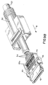
- Figure 9 shows how terminal module 36 (Fig. 8) might be used in an electrical connector.
- the terminal module is inserted into the rear of a dielectric or insulating housing 40 such that terminal portions 30 are disposed within a forwardly projecting plug portion 42 of the housing, and terminal portions 28a and 28b projecting rearwardly between wing portions 44 of the housing.
- terminal portions 28a and 28b are disposed in different planes and, thereby, define a mouth therebetween and into which a narrow circuit board 48 is inserted in the direction of arrows "A". Therefore, terminal portions 28a (28b) form solder pads for soldering to a plurality of parallel conductors or circuit traces 48a on opposite sides of circuit board 48.
- FIG. 9A The subassembly of Figure 9A then can be assembled in an electrical connector as shown in Figure 9B.
- a boot 50 is slipped onto a multi-conductor cable 52.
- the cable includes a plurality of discrete electrical wires 54.
- the insulating cladding of the wires is removed to expose lengths of the conductive cores of the wires.
- the exposed cores then are soldered to conductors 48a of circuit board 48 to thereby electrically connect the conductive cores of the electrical wires of cable 52 to terminal portions 28a and 28b of terminal module 36 within the connector assembly.
- Boot 50 then is moved forwardly in the direction of arrow "B" into latching engagement with latches 56 to form the completed electrical connector assembly.
Landscapes
- Engineering & Computer Science (AREA)
- Manufacturing & Machinery (AREA)
- Manufacturing Of Electrical Connectors (AREA)
- Coupling Device And Connection With Printed Circuit (AREA)
Applications Claiming Priority (2)
| Application Number | Priority Date | Filing Date | Title |
|---|---|---|---|
| US16851 | 1998-01-30 | ||
| US09/016,851 US6453552B1 (en) | 1998-01-30 | 1998-01-30 | Method of manufacturing electrical terminals and terminal modules |
Publications (2)
| Publication Number | Publication Date |
|---|---|
| EP0933840A2 true EP0933840A2 (de) | 1999-08-04 |
| EP0933840A3 EP0933840A3 (de) | 2001-11-07 |
Family
ID=21779327
Family Applications (1)
| Application Number | Title | Priority Date | Filing Date |
|---|---|---|---|
| EP99100477A Withdrawn EP0933840A3 (de) | 1998-01-30 | 1999-01-12 | Herstellungsverfahren für elektrische Endstücke und Endstückmodule |
Country Status (7)
| Country | Link |
|---|---|
| US (1) | US6453552B1 (de) |
| EP (1) | EP0933840A3 (de) |
| KR (1) | KR100296893B1 (de) |
| CN (1) | CN1155146C (de) |
| MY (1) | MY122427A (de) |
| SG (1) | SG75149A1 (de) |
| TW (1) | TW402831B (de) |
Families Citing this family (16)
| Publication number | Priority date | Publication date | Assignee | Title |
|---|---|---|---|---|
| WO2000037766A2 (en) * | 1998-12-22 | 2000-06-29 | Weatherford/Lamb, Inc. | Procedures and equipment for profiling and jointing of pipes |
| US6764336B2 (en) * | 2001-02-27 | 2004-07-20 | Hon Hai Precision Ind. Co., Ltd. | Method for forming an electrical connector and an electrical connector obtained thereby |
| GB0119977D0 (en) * | 2001-08-16 | 2001-10-10 | E2 Tech Ltd | Apparatus and method |
| US7156179B2 (en) * | 2001-09-07 | 2007-01-02 | Weatherford/Lamb, Inc. | Expandable tubulars |
| JP4026605B2 (ja) * | 2004-03-01 | 2007-12-26 | 松下電工株式会社 | 電線接続用コネクタの製造方法 |
| US7503396B2 (en) * | 2006-02-15 | 2009-03-17 | Weatherford/Lamb | Method and apparatus for expanding tubulars in a wellbore |
| US8104173B2 (en) | 2008-04-08 | 2012-01-31 | Delphi Technologies, Inc. | Method for manufacturing a series of electric terminals |
| CN201294322Y (zh) * | 2008-09-08 | 2009-08-19 | 东莞长安旭竤电子制品厂 | Hdmi端子料带 |
| CN101552421B (zh) * | 2009-05-18 | 2011-01-05 | 安徽汇精模具研发科技有限公司 | 低压电器双层接线终端连续模 |
| JP5009972B2 (ja) * | 2009-12-21 | 2012-08-29 | 日立オートモティブシステムズ株式会社 | コネクタの製造方法 |
| KR101185502B1 (ko) | 2011-04-06 | 2012-09-24 | 미성텔레컴(주) | 프레스 핏트 카드에지 커넥터용 단자 및 그 제조방법 |
| TW201401696A (zh) * | 2012-06-27 | 2014-01-01 | Golden Transmart Internat Co Ltd | 萬用序列匯流排母座連接器之製造方法 |
| TWM588383U (zh) * | 2019-05-02 | 2019-12-21 | 矽瑪科技股份有限公司 | 具兩件式膠體嵌接結構之視頻連接器 |
| CN113258325A (zh) * | 2020-01-28 | 2021-08-13 | 富加宜(美国)有限责任公司 | 高频中板连接器 |
| USD1103122S1 (en) * | 2024-03-29 | 2025-11-25 | Dinkle Enterprise Co., Ltd. | Connector spacer |
| USD1096655S1 (en) * | 2024-09-09 | 2025-10-07 | Dinkle Enterprise Co., Ltd. | Clamping terminal of connector |
Family Cites Families (14)
| Publication number | Priority date | Publication date | Assignee | Title |
|---|---|---|---|---|
| US4021095A (en) | 1974-02-21 | 1977-05-03 | Amp Incorporated | Stacked carrier strip assembly |
| JPS5826764B2 (ja) | 1978-10-31 | 1983-06-04 | 新光電気工業株式会社 | 多接点接触ばねの製造方法 |
| US4442594A (en) | 1980-12-30 | 1984-04-17 | Thomas & Betts Corporation | Method for making an electrical connector |
| US4428642A (en) | 1982-01-11 | 1984-01-31 | Litton Systems, Inc. | Body-carry electrical contact strips |
| JPS5927485A (ja) | 1982-08-09 | 1984-02-13 | ソニー株式会社 | 基板用コネクタの製造方法 |
| JPS60101888A (ja) * | 1983-10-31 | 1985-06-05 | アンプ インコーポレーテッド | 電気コネクタ |
| JPH0541265A (ja) * | 1991-08-01 | 1993-02-19 | Tanaka Kikinzoku Kogyo Kk | ハンドラー用コンタクトピンの製造方法 |
| GB9324064D0 (en) * | 1993-11-23 | 1994-01-12 | Amp Gmbh | Grounding electrical leads |
| JPH0864315A (ja) * | 1994-08-02 | 1996-03-08 | Molex Inc | リセプタクル型電気コネクタ |
| JPH08273798A (ja) * | 1995-03-30 | 1996-10-18 | Japan Aviation Electron Ind Ltd | Smtコネクタ用コンタクトの製造方法 |
| JPH0992426A (ja) * | 1995-09-21 | 1997-04-04 | Matsushita Electric Ind Co Ltd | リード端子の製造方法 |
| US5722861A (en) * | 1996-02-28 | 1998-03-03 | Molex Incorporated | Electrical connector with terminals of varying lengths |
| JP3638713B2 (ja) * | 1996-05-15 | 2005-04-13 | 株式会社オートネットワーク技術研究所 | 基板用の接続端子中間品および接続端子付き基板 |
| US5848920A (en) * | 1996-07-16 | 1998-12-15 | Molex Incorporated | Fabrication of electrical terminals for edge card connectors |
-
1998
- 1998-01-30 US US09/016,851 patent/US6453552B1/en not_active Expired - Fee Related
- 1998-12-29 SG SG1998005966A patent/SG75149A1/en unknown
-
1999
- 1999-01-04 TW TW088100030A patent/TW402831B/zh not_active IP Right Cessation
- 1999-01-12 EP EP99100477A patent/EP0933840A3/de not_active Withdrawn
- 1999-01-28 KR KR1019990002794A patent/KR100296893B1/ko not_active Expired - Fee Related
- 1999-01-29 MY MYPI99000324A patent/MY122427A/en unknown
- 1999-01-29 CN CNB99101720XA patent/CN1155146C/zh not_active Expired - Fee Related
Also Published As
| Publication number | Publication date |
|---|---|
| MY122427A (en) | 2006-04-29 |
| US6453552B1 (en) | 2002-09-24 |
| CN1224938A (zh) | 1999-08-04 |
| KR19990072312A (ko) | 1999-09-27 |
| KR100296893B1 (ko) | 2001-07-12 |
| EP0933840A3 (de) | 2001-11-07 |
| CN1155146C (zh) | 2004-06-23 |
| SG75149A1 (en) | 2000-09-19 |
| TW402831B (en) | 2000-08-21 |
Similar Documents
| Publication | Publication Date | Title |
|---|---|---|
| US6453552B1 (en) | Method of manufacturing electrical terminals and terminal modules | |
| US4292736A (en) | Method for making jack type receptacles | |
| US5964620A (en) | Insulation displacement connector | |
| EP0261905B1 (de) | Elektrischer Verbinder und Verfahren zur Verbindung von Adern an diesem | |
| CN110932006A (zh) | 电连接器及其制造方法 | |
| WO2007127467A2 (en) | Insulation displacement terminal | |
| GB2037493A (en) | Insulation displacing contact for electrical connector | |
| US6406338B1 (en) | Board terminal and method of producing same | |
| US4113338A (en) | Insulation-piercing contact | |
| US6431903B1 (en) | Insulation displacement contact for use with fine wires | |
| US20020002007A1 (en) | Board terminal and method of producing same | |
| US4187606A (en) | Flexible electrical jumper and method of making same | |
| CN100394514C (zh) | 扁形电缆 | |
| US8272901B2 (en) | Crimp contacts and electrical connector assemblies including the same | |
| US5208978A (en) | Method of fabricating an electrical terminal pin | |
| EP0568907B1 (de) | Elektrischer Anschlussstift | |
| EP0570832B1 (de) | Verbindergehäuseanordnung für einzelne Drähte | |
| EP1429429B1 (de) | Verfahren zur Herstellung von Steckstiften und die Steckstifte selbst | |
| US11489307B1 (en) | Method of crimping an electrical terminal onto a flat flexible cable | |
| EP0924811A1 (de) | Systemträger, und Verfahren zum Herstellen eines Systemträgers | |
| US6176730B1 (en) | Electrical connection cable and manufacturing method thereof | |
| JPH07220792A (ja) | 雌型端子およびその製造方法 | |
| US4266843A (en) | Insulation displacing electrical contact and method of making same | |
| EP0125098A1 (de) | Verfahren zur Herstellung von elektrisch leitenden Stiften | |
| JPH06208858A (ja) | 同軸ケーブル接続装置 |
Legal Events
| Date | Code | Title | Description |
|---|---|---|---|
| PUAI | Public reference made under article 153(3) epc to a published international application that has entered the european phase |
Free format text: ORIGINAL CODE: 0009012 |
|
| AK | Designated contracting states |
Kind code of ref document: A2 Designated state(s): AT BE CH CY DE DK ES FI FR GB GR IE IT LI LU MC NL PT SE Kind code of ref document: A2 Designated state(s): DE FR GB IT |
|
| AX | Request for extension of the european patent |
Free format text: AL;LT;LV;MK;RO;SI |
|
| PUAL | Search report despatched |
Free format text: ORIGINAL CODE: 0009013 |
|
| AK | Designated contracting states |
Kind code of ref document: A3 Designated state(s): AT BE CH CY DE DK ES FI FR GB GR IE IT LI LU MC NL PT SE |
|
| AX | Request for extension of the european patent |
Free format text: AL;LT;LV;MK;RO;SI |
|
| 17P | Request for examination filed |
Effective date: 20020427 |
|
| AKX | Designation fees paid |
Free format text: DE FR GB IT |
|
| STAA | Information on the status of an ep patent application or granted ep patent |
Free format text: STATUS: THE APPLICATION HAS BEEN WITHDRAWN |
|
| 18W | Application withdrawn |
Effective date: 20021211 |