EP0936455A2 - Halbleiterdrucksensor - Google Patents
Halbleiterdrucksensor Download PDFInfo
- Publication number
- EP0936455A2 EP0936455A2 EP98120577A EP98120577A EP0936455A2 EP 0936455 A2 EP0936455 A2 EP 0936455A2 EP 98120577 A EP98120577 A EP 98120577A EP 98120577 A EP98120577 A EP 98120577A EP 0936455 A2 EP0936455 A2 EP 0936455A2
- Authority
- EP
- European Patent Office
- Prior art keywords
- hole
- base
- base plate
- package
- semiconductor pressure
- Prior art date
- Legal status (The legal status is an assumption and is not a legal conclusion. Google has not performed a legal analysis and makes no representation as to the accuracy of the status listed.)
- Granted
Links
Images

Classifications
-
- G—PHYSICS
- G01—MEASURING; TESTING
- G01L—MEASURING FORCE, STRESS, TORQUE, WORK, MECHANICAL POWER, MECHANICAL EFFICIENCY, OR FLUID PRESSURE
- G01L19/00—Details of, or accessories for, apparatus for measuring steady or quasi-steady pressure of a fluent medium insofar as such details or accessories are not special to particular types of pressure gauges
- G01L19/14—Housings
- G01L19/147—Details about the mounting of the sensor to support or covering means
Definitions
- the present invention relates to a strain gauge type semiconductor pressure detecting device for detecting relatively high pressure.
- a strain gauge type semiconductor pressure detecting device of the prior art is disclosed, for example, in Japanese Non-examined Patent Publication No. 7-294353.
- the semiconductor pressure detecting device disclosed in this publication has a pressure sensor chip 104 mounted in a recess 101b, formed in a body 101, via a metal base 102 (which corresponds to a base plate of the present invention) and a glass base 103, wherein pressure is introduced via through holes 101a, 102a, 103a made in the body 101, the metal base 102 and the glass base 103, respectively, to be concentric with each other, and is applied to the pressure sensor chip 104.
- a circular groove 102b concentric with the through hole 102a is formed inside the laser-welded portion in this prior art example, thereby making the central portion relatively raised so that the glass base 103 and the pressure sensor chip 104 are not subject to undesirable stress caused by thermal expansion of components due to the heat of laser welding.
- the semiconductor pressure detecting device of the prior art has such a problem that since the laser welding step takes much time, the device can not produced at low cost.
- Use of the projection welding step may be conceived to counter this problem, but this causes another problem that impact generated during bonding or residual thermal stress may cause breakage in the joint of the base.
- An object of the present invention is to solve the above problems of the prior art and to provide a semiconductor pressure detecting device of low cost and high reliability, which is capable of measuring relatively high pressure.
- a first semiconductor pressure detecting device comprises a package having a pressure introducing hole; a base plate which has a first through hole made at the center thereof and is mounted in the package so that the first through hole is disposed substantially concentrically with the pressure introducing hole; a base which has a second through hole made at the center thereof and is mounted on the base plate so that the second through hole is disposed substantially concentrically with the first through hole; and a semiconductor pressure sensor chip which is mounted on the base and detects a pressure introduced through the pressure introducing hole and the first and second through holes; wherein the base plate has a thickened portion formed around the first through hole and is fixed by welding the circumference of the thickened portion onto the package.
- the thickened portion formed in the base plate makes it possible to prevent the base plate from deforming in the thickened portion under a pressure applied thereto.
- cross section of the base has a rectangular shape and cross section of the thickened portion is a circle of a diameter substantially equal to the diagonal of the rectangular, with the base being mounted right above the thickened portion.
- a second semiconductor pressure detecting device comprises a package having a pressure introducing hole; a base plate which has a first through hole made at the center thereof and is mounted in the package so that the first through hole is disposed substantially concentrically with the pressure introducing hole; a base which has a second through hole made at the center thereof and is mounted on the base plate so that the second through hole is disposed substantially concentrically with the first through hole; and a semiconductor pressure sensor chip which is mounted on the base and detects a pressure introduced through the pressure introducing hole and the first and second through holes; wherein the base plate has a ring placed to surround the first through hole to be concentric with the first through hole and is fixed by welding the circumference of the ring onto the package.
- the ring provided on the base plate makes it possible to prevent the portion of the base plate right above the ring from deforming under a pressure applied thereto.
- cross section of the base has a profile substantially matching that of the cross section of the ring and the base is mounted right above the ring.
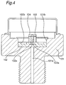
- Fig. 1 is a schematic cross sectional view showing the configuration of a semiconductor pressure sensor according to one embodiment of the present invention.
- the semiconductor pressure sensor comprises a semiconductor pressure sensor chip 1 mounted in a package 4 as described below.
- the thickened portion 7 is preferably smaller across as far as such a condition is satisfied as the base 2 is located within the thickened portion 7 of the base plate 3.
- the present invention is embodied by using the circular thickened portion 7 and the base 2 having rectangular cross section, preferably outer diameter of the thickened portion 7 and the diagonal of the cross section of the base 2 are substantially the same.
- the present invention is embodied by using the thickened portion 7 having rectangular cross section and the base 2 having rectangular cross section, preferably the thickened portion 7 and the base 2 have substantially the same cross sectional configuration.
- substantially the same means that the difference between two dimensions is not greater than about 0.5 mm which is the tolerable variation in production such as the assembly step.
- Cross sectional profile of the thickened portion 7 may be either greater or smaller than the cross sectional profile of the base 2, as far as such a condition is satisfied that the stress generated in the base 2 due to warping of the base plate 3 is less than the fracture stress. Whether the condition that the stress generated in the base 2 due to warping of the base plate 3 is less than the fracture stress is satisfied or not is determined by such factors as the shapes of the thickened portion 7 and the base 2, materials used to make the base plate 3 and the base 2 and the maximum possible pressure applied, among others.
- the package body 4a constructed as described above is fitted with the base plate 3, the base 2, the semiconductor pressure sensor chip 1, the circuit board 50 and necessary interconnections, with the package cover placed thereon to complete the semiconductor pressure sensor of the embodiment.
- the base plate 3 is placed on the package body 4a so that the thickened portion 7 is located within the first recess 43 and the through hole 30 becomes substantially concentric with the pressure introducing hole 40, and is then fixed by projection welding of the thin portion 5 and the ridge 6.
- the base 2 is fixed by bonding onto the base plate 3 so that the through hole 20 becomes substantially concentric with the through hole 30.
- the semiconductor pressure sensor chip 1 is fixed onto the base 2 by means of an adhesive or the like so that the thin portion whereon the diffused resistor is formed is located right above the through hole 20.
- the semiconductor pressure sensor chip is fitted with necessary internal wiring by means of wire bonding or the like, with detection signal being output via the circuit board 50 and an output terminal 51.
- the semiconductor pressure sensor of this embodiment configured as described above has the thickened portion 7 formed at the joint of the base 2 with the base plate 3, and is therefore capable of minimizing the warp of the base plate (thickened portion) located right below the base 2 even when a relatively high pressure is applied to the base plate 3, thereby making it possible to measure high pressures.
- the semiconductor pressure sensor of this embodiment configured as described above has the thickened portion 7 formed at the joint of the base 2 with the base plate 3, stress caused by impact and heat during welding is prevented from being transmitted to the base 2, thereby preventing the joint of the base 2 and the base plate 3 from breaking. Consequently, the semiconductor pressure sensor of this embodiment can be produced by employing projection welding step which can be completed in a relatively short period of time compared to laser welding, resulting in a lower production cost.
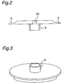
- a ring 8 may be attached onto the base plate on the side opposite to the base by brazing or other method. Similar effects as those of the embodiment described previously can be achieved also with this configuration, and a ring of appropriate width and height determined according to the purpose can be used thus allowing for greater degree of freedom in design.
- a ring of appropriate width and height determined according to the purpose can be used thus allowing for greater degree of freedom in design.
- the thickened portion 7 is formed on the base plate as in the embodiment shown in Fig. 1, there is a limitation on the thickness of the thickened portion 7 when the base plate is made by punching with a press and a die, there is no such limitation when the separate ring 8 is attached.
- Fig. 3 is a perspective view showing the base plate of this variation of the embodiment up side down.
- the first semiconductor pressure detecting device comprises the package having the pressure introducing hole, the base plate which has the first through hole made at the center thereof and is mounted in the package so that the first through hole is disposed concentrically with the pressure introducing hole, the base which has the second through hole made at the center thereof and is mounted on the base plate so that the second through hole is disposed substantially concentrically with the first through hole, and the semiconductor pressure sensor chip mounted on the base.
- the base plate has the thickened portion formed around the first through hole and is fixed by welding the circumference of the thickened portion onto the package, thereby making it possible to prevent the base plate from deforming in the thickened portion under a pressure applied thereto.
- the first semiconductor pressure detecting device can be produced by projection welding which requires shorter period of time, resulting in lower production cost. Also because the semiconductor pressure sensor chip can be prevented from experiencing undesirable stress when a pressure is applied during operation, reliability can be improved and relatively high pressure can be measured.
- the semiconductor pressure sensor chip can be effectively prevented from experiencing undesirable stress when a pressure is applied, and therefore reliability can be improved and relatively high pressure can be measured.
- the second semiconductor pressure detecting device has a ring mounted on the base plate to surround the first through hole concentrically with the first through hole, and the base plate is fixed by welding the circumference of the ring onto the package, thus making it possible to reduce the deformation of the portion of the base plate right above the ring under a pressure applied thereto.
- the second semiconductor pressure detecting device can be produced by projection welding step which requires shorter period of time, resulting in lower production cost. Also because the semiconductor pressure sensor chip can be prevented from experiencing undesirable stress when a pressure is applied during operation, reliability can be improved and relatively high pressure can be measured.
- the cross section of the base has a profile substantially matching that of the cross section of the ring and the base is mounted right above the ring, the semiconductor pressure sensor chip can be more effectively prevented from experiencing undesirable stress when a pressure is applied, and therefore reliability can be improved and relatively high pressure can be measured.
Landscapes
- Chemical & Material Sciences (AREA)
- Analytical Chemistry (AREA)
- Physics & Mathematics (AREA)
- General Physics & Mathematics (AREA)
- Measuring Fluid Pressure (AREA)
- Pressure Sensors (AREA)
Applications Claiming Priority (2)
| Application Number | Priority Date | Filing Date | Title |
|---|---|---|---|
| JP10034548A JPH11230845A (ja) | 1998-02-17 | 1998-02-17 | 半導体圧力検出装置 |
| JP3454898 | 1998-02-17 |
Publications (3)
| Publication Number | Publication Date |
|---|---|
| EP0936455A2 true EP0936455A2 (de) | 1999-08-18 |
| EP0936455A3 EP0936455A3 (de) | 2000-04-05 |
| EP0936455B1 EP0936455B1 (de) | 2004-01-07 |
Family
ID=12417375
Family Applications (1)
| Application Number | Title | Priority Date | Filing Date |
|---|---|---|---|
| EP98120577A Expired - Lifetime EP0936455B1 (de) | 1998-02-17 | 1998-10-30 | Halbleiterdrucksensor |
Country Status (4)
| Country | Link |
|---|---|
| US (1) | US6127713A (de) |
| EP (1) | EP0936455B1 (de) |
| JP (1) | JPH11230845A (de) |
| DE (1) | DE69820981T2 (de) |
Cited By (2)
| Publication number | Priority date | Publication date | Assignee | Title |
|---|---|---|---|---|
| WO2004001358A1 (de) * | 2002-06-22 | 2003-12-31 | Robert Bosch Gmbh | Hochdruck-sensor mit silizium-membran und lotschicht |
| CN102620880A (zh) * | 2012-03-31 | 2012-08-01 | 浙江理工大学 | 测量激波加载固定颗粒群非稳态力的传感器固定装置 |
Families Citing this family (6)
| Publication number | Priority date | Publication date | Assignee | Title |
|---|---|---|---|---|
| CN103926029B (zh) * | 2014-04-28 | 2016-03-30 | 中国电子科技集团公司第四十九研究所 | 压阻式压力传感器敏感芯片气密性硬封装方法 |
| KR101593093B1 (ko) * | 2014-06-27 | 2016-02-18 | 주식회사 현대케피코 | 압력측정장치 |
| DE102014119396A1 (de) * | 2014-12-22 | 2016-06-23 | Endress + Hauser Gmbh + Co. Kg | Druckmesseinrichtung |
| DE102015117736A1 (de) * | 2015-10-19 | 2017-04-20 | Endress+Hauser Gmbh+Co. Kg | Druckmesseinrichtung |
| US10640374B2 (en) * | 2017-05-18 | 2020-05-05 | Dunan Microstaq, Inc. | Method and structure of attachment layer for reducing stress transmission to attached MEMS die |
| US10495538B2 (en) * | 2017-09-18 | 2019-12-03 | Measurement Specialties, Inc | Modular sensor package having adhesive-free seal to housing |
Family Cites Families (10)
| Publication number | Priority date | Publication date | Assignee | Title |
|---|---|---|---|---|
| JPS6272178A (ja) * | 1985-09-26 | 1987-04-02 | Nippon Denso Co Ltd | 半導体圧力検出装置およびその製造方法 |
| JPH0269630A (ja) * | 1988-09-05 | 1990-03-08 | Nippon Denso Co Ltd | 半導体圧力センサ |
| JP2503290B2 (ja) * | 1990-05-21 | 1996-06-05 | 株式会社日立製作所 | 半導体圧力・差圧測定ダイヤフラム |
| US5119196A (en) * | 1990-06-25 | 1992-06-02 | At&T Bell Laboratories | Ghost cancellation of analog tv signals |
| IL106790A (en) * | 1992-09-01 | 1996-08-04 | Rosemount Inc | A capacitive pressure sensation consisting of the bracket and the process of creating it |
| JPH06125096A (ja) * | 1992-10-09 | 1994-05-06 | Mitsubishi Electric Corp | 半導体圧力センサ |
| JP3365038B2 (ja) * | 1994-04-28 | 2003-01-08 | 松下電工株式会社 | 圧力センサ |
| JPH07294354A (ja) * | 1994-04-28 | 1995-11-10 | Nippondenso Co Ltd | 半導体圧力センサ |
| FR2738340B1 (fr) * | 1995-08-28 | 1997-11-21 | Europ Propulsion | Architecture d'integration d'un element sensible dans un capteur de pression |
| JPH09222372A (ja) * | 1996-02-19 | 1997-08-26 | Mitsubishi Electric Corp | 半導体式センサ |
-
1998
- 1998-02-17 JP JP10034548A patent/JPH11230845A/ja active Pending
- 1998-10-29 US US09/181,929 patent/US6127713A/en not_active Expired - Fee Related
- 1998-10-30 EP EP98120577A patent/EP0936455B1/de not_active Expired - Lifetime
- 1998-10-30 DE DE69820981T patent/DE69820981T2/de not_active Expired - Fee Related
Cited By (5)
| Publication number | Priority date | Publication date | Assignee | Title |
|---|---|---|---|---|
| WO2004001358A1 (de) * | 2002-06-22 | 2003-12-31 | Robert Bosch Gmbh | Hochdruck-sensor mit silizium-membran und lotschicht |
| US7152483B2 (en) | 2002-06-22 | 2006-12-26 | Robert Bosch Gmbh | High pressure sensor comprising silicon membrane and solder layer |
| RU2324158C2 (ru) * | 2002-06-22 | 2008-05-10 | Роберт Бош Гмбх | Устройство для измерения давления |
| CN102620880A (zh) * | 2012-03-31 | 2012-08-01 | 浙江理工大学 | 测量激波加载固定颗粒群非稳态力的传感器固定装置 |
| CN102620880B (zh) * | 2012-03-31 | 2013-11-06 | 浙江理工大学 | 测量激波加载固定颗粒群非稳态力的传感器固定装置 |
Also Published As
| Publication number | Publication date |
|---|---|
| EP0936455A3 (de) | 2000-04-05 |
| US6127713A (en) | 2000-10-03 |
| DE69820981D1 (de) | 2004-02-12 |
| DE69820981T2 (de) | 2004-10-28 |
| EP0936455B1 (de) | 2004-01-07 |
| JPH11230845A (ja) | 1999-08-27 |
Similar Documents
| Publication | Publication Date | Title |
|---|---|---|
| US6062088A (en) | Pressure sensor | |
| US5625151A (en) | Silicone oil-filled semiconductor pressure sensor | |
| EP1316786B1 (de) | Drucksensor des kapazitätstyps und verfahren zu seiner herstellung | |
| US7093493B2 (en) | Pressure sensor having a silicon chip on a steel diaphragm | |
| US5604363A (en) | Semiconductor pressure sensor with package | |
| US5721446A (en) | Semiconductor pressure sensor with spacing member disposed between sensor and substrate | |
| JP2503290B2 (ja) | 半導体圧力・差圧測定ダイヤフラム | |
| US8127617B2 (en) | Pressure sensor, manufacturing method thereof, and electronic component provided therewith | |
| JP2012500974A (ja) | センサデバイスパッケージ及び方法 | |
| US6127713A (en) | Semiconductor pressure detecting device | |
| CN116577003A (zh) | 一种轴力传感器 | |
| JP3915605B2 (ja) | 圧力センサ装置 | |
| US5191798A (en) | Pressure sensor | |
| US6591686B1 (en) | Oil filled pressure transducer | |
| JPH07101747B2 (ja) | 半導体圧力センサ | |
| JPH11304612A (ja) | 半導体圧力検出装置 | |
| US6021673A (en) | Semiconductor pressure detecting device | |
| US4400682A (en) | Pressure sensor | |
| JP3365038B2 (ja) | 圧力センサ | |
| CN219416519U (zh) | 一种轴力传感器 | |
| JP3220346B2 (ja) | 圧力センサ及びその製造方法 | |
| JP3876615B2 (ja) | 半導体加速度センサ | |
| JP4168813B2 (ja) | 圧力センサ装置 | |
| JP4019966B2 (ja) | 圧力センサ装置 | |
| JPH04267566A (ja) | 高圧用半導体圧力センサ |
Legal Events
| Date | Code | Title | Description |
|---|---|---|---|
| PUAI | Public reference made under article 153(3) epc to a published international application that has entered the european phase |
Free format text: ORIGINAL CODE: 0009012 |
|
| AK | Designated contracting states |
Kind code of ref document: A2 Designated state(s): DE ES FR GB IT NL |
|
| AX | Request for extension of the european patent |
Free format text: AL;LT;LV;MK;RO;SI |
|
| PUAL | Search report despatched |
Free format text: ORIGINAL CODE: 0009013 |
|
| AK | Designated contracting states |
Kind code of ref document: A3 Designated state(s): AT BE CH CY DE DK ES FI FR GB GR IE IT LI LU MC NL PT SE |
|
| AX | Request for extension of the european patent |
Free format text: AL;LT;LV;MK;RO;SI |
|
| 17P | Request for examination filed |
Effective date: 20000721 |
|
| AKX | Designation fees paid |
Free format text: DE ES FR GB IT NL |
|
| 17Q | First examination report despatched |
Effective date: 20021113 |
|
| GRAH | Despatch of communication of intention to grant a patent |
Free format text: ORIGINAL CODE: EPIDOS IGRA |
|
| GRAS | Grant fee paid |
Free format text: ORIGINAL CODE: EPIDOSNIGR3 |
|
| GRAA | (expected) grant |
Free format text: ORIGINAL CODE: 0009210 |
|
| AK | Designated contracting states |
Kind code of ref document: B1 Designated state(s): DE ES FR GB IT NL |
|
| PG25 | Lapsed in a contracting state [announced via postgrant information from national office to epo] |
Ref country code: NL Free format text: LAPSE BECAUSE OF FAILURE TO SUBMIT A TRANSLATION OF THE DESCRIPTION OR TO PAY THE FEE WITHIN THE PRESCRIBED TIME-LIMIT Effective date: 20040107 |
|
| REG | Reference to a national code |
Ref country code: GB Ref legal event code: FG4D |
|
| REF | Corresponds to: |
Ref document number: 69820981 Country of ref document: DE Date of ref document: 20040212 Kind code of ref document: P |
|
| PG25 | Lapsed in a contracting state [announced via postgrant information from national office to epo] |
Ref country code: ES Free format text: LAPSE BECAUSE OF FAILURE TO SUBMIT A TRANSLATION OF THE DESCRIPTION OR TO PAY THE FEE WITHIN THE PRESCRIBED TIME-LIMIT Effective date: 20040418 |
|
| NLV1 | Nl: lapsed or annulled due to failure to fulfill the requirements of art. 29p and 29m of the patents act | ||
| ET | Fr: translation filed | ||
| PLBE | No opposition filed within time limit |
Free format text: ORIGINAL CODE: 0009261 |
|
| STAA | Information on the status of an ep patent application or granted ep patent |
Free format text: STATUS: NO OPPOSITION FILED WITHIN TIME LIMIT |
|
| 26N | No opposition filed |
Effective date: 20041008 |
|
| PGFP | Annual fee paid to national office [announced via postgrant information from national office to epo] |
Ref country code: GB Payment date: 20061025 Year of fee payment: 9 |
|
| PGFP | Annual fee paid to national office [announced via postgrant information from national office to epo] |
Ref country code: DE Payment date: 20061026 Year of fee payment: 9 |
|
| PGFP | Annual fee paid to national office [announced via postgrant information from national office to epo] |
Ref country code: IT Payment date: 20061031 Year of fee payment: 9 |
|
| GBPC | Gb: european patent ceased through non-payment of renewal fee |
Effective date: 20071030 |
|
| PG25 | Lapsed in a contracting state [announced via postgrant information from national office to epo] |
Ref country code: DE Free format text: LAPSE BECAUSE OF NON-PAYMENT OF DUE FEES Effective date: 20080501 |
|
| REG | Reference to a national code |
Ref country code: FR Ref legal event code: ST Effective date: 20080630 |
|
| PGFP | Annual fee paid to national office [announced via postgrant information from national office to epo] |
Ref country code: FR Payment date: 20061010 Year of fee payment: 9 |
|
| PG25 | Lapsed in a contracting state [announced via postgrant information from national office to epo] |
Ref country code: GB Free format text: LAPSE BECAUSE OF NON-PAYMENT OF DUE FEES Effective date: 20071030 |
|
| PG25 | Lapsed in a contracting state [announced via postgrant information from national office to epo] |
Ref country code: FR Free format text: LAPSE BECAUSE OF NON-PAYMENT OF DUE FEES Effective date: 20071031 |
|
| PG25 | Lapsed in a contracting state [announced via postgrant information from national office to epo] |
Ref country code: IT Free format text: LAPSE BECAUSE OF NON-PAYMENT OF DUE FEES Effective date: 20071030 |