EP0936625A2 - Assoziativspeicher (CAM) - Google Patents
Assoziativspeicher (CAM) Download PDFInfo
- Publication number
- EP0936625A2 EP0936625A2 EP99200438A EP99200438A EP0936625A2 EP 0936625 A2 EP0936625 A2 EP 0936625A2 EP 99200438 A EP99200438 A EP 99200438A EP 99200438 A EP99200438 A EP 99200438A EP 0936625 A2 EP0936625 A2 EP 0936625A2
- Authority
- EP
- European Patent Office
- Prior art keywords
- data
- cam
- cam array
- row
- bit
- Prior art date
- Legal status (The legal status is an assumption and is not a legal conclusion. Google has not performed a legal analysis and makes no representation as to the accuracy of the status listed.)
- Withdrawn
Links
Images
Classifications
-
- G—PHYSICS
- G11—INFORMATION STORAGE
- G11C—STATIC STORES
- G11C15/00—Digital stores in which information comprising one or more characteristic parts is written into the store and in which information is read-out by searching for one or more of these characteristic parts, i.e. associative or content-addressed stores
- G11C15/04—Digital stores in which information comprising one or more characteristic parts is written into the store and in which information is read-out by searching for one or more of these characteristic parts, i.e. associative or content-addressed stores using semiconductor elements
Definitions
- the present invention relates generally to computer memories, and more particularly to a content addressable memory with reduced size, power, and access time and increased floor planning flexibility.
- Random access memory is the memory most often used in current electronic systems.
- the address of data is provided on an address bus and the corresponding data is then retrieved.
- the width of the address bus determines how many memory locations can be addressed and thus determines the size of the memory.
- CAM content addressable memory
- the data itself is provided in a special register.
- the CAM is then searched for the data by comparing each bit of the data with each bit of the information stored in the CAM. If a match is found, a match flag is set to indicate that the data was found.
- a priority encoder then prioritizes the matching locations (if more than one match was found) and generates the corresponding address of the highest priority matching location.
- One application for the CAM is in a memory cache system in which the matching process is used to determine whether the cache includes data needed elsewhere, such as data requested by a processor.
- the CAM Since the CAM is searched based on the contents of the memory location rather than based on the data location in the memory, and further, since the same data content may be found in more than one location in the CAM, the CAM is also useful in applications in which it is desirable to retrieve multiple items from memory simultaneously.
- the highly parallel nature of content addressing is also an advantageous feature useful, for example, in processing high level algorithmic functions.
- Use of the CAM in these types of applications also generally requires much larger CAMs than typically used in a cache. For smaller CAMs such as those used in cache applications, a primary concern is fast, efficient access and thus, the focus is on optimizing the access method to minimize latency. In larger CAMs, however, where the objective is to support a large number of entries, attention must be focused on maintaining an efficient layout shape and a reasonable bandwidth.
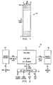
- Fig. 1 shows an architectural diagram of a prior art CAM array 100.
- the prior art CAM array 100 consists of 1024 words, each word having 56 bits. Each row in the CAM array 100 represents one of the 1024 words. Each of the 56 columns in the CAM array 100 represents one bit in each of the 1024 words.
- a long, narrow memory structure is typically used.
- the CAM array may be extended to increase memory capacity by adding more rows. This long, narrow structure, however, not only becomes increasingly cumbersome as more capacity is added but also severely impacts the layout of the floor plan of any device in which it is used.
- the present invention is a content addressable memory (CAM) system, having a CAM array operable to store a number of data words, each of the data words having a number of bits.
- the CAM is made up of rows and columns of CAM cells, each CAM cell operable to store one of the bits of one of the data words.
- Each row of the CAM system of the present invention stores the bits of at least two of the data words. The bits of the at least two data words on a single row are interleaved.
- the CAM system of the present invention accesses each of the data words on the row in turn during one of a number of cycles.
- a portion of the content of the data words is used to determine where on the row the data word is stored and, thus, reduces the number of cycles required to search for a particular data word.
- Fig. 2 illustrates a CAM system 50 in accordance with the present invention.
- the CAM system 50 shown in Fig. 2 includes a CAM array 52 which, although other similarly proportioned dimensions can be used as will be understood from the description hereinbelow, is comprised of 57,344 CAM cells arranged in 256 rows and 224 columns.
- the CAM array 52 is bidirectionally coupled to a bit line controller 54 by 224 bit line pairs, each bit line pair connecting one of the columns of CAM cells in the CAM array 52.
- the 224 bit line pairs are selectively enabled by the bit line controller 54 in one embodiment of the present invention in accordance with a 2-bit 'column address" signal and a 'mode control' signal.
- the ⁇ column address' signal being provided by a cycle counter, not shown.
- the 224 bit line pairs are selectively enabled by the bit line controller 54 in accordance with the 'column address' signal, the 'mode control' signal and a 56-bit 'data in' signal.
- the 56-bit 'data in' signal provides data to be stored in or matched to data stored in the CAM array 56.
- a 56-bit 'data out' signal returns data retrieved from the CAM array 52.
- the CAM array 52 is also connected to an address decoder 53 by 256 row select lines and to a priority encoder 58 by 256 match lines.
- the 256 row select lines are each connected to one row of CAM cells in the CAM array 52 which are selectively enabled in accordance with a 8-bit 'row address in' signal decoded by the address decoder 53.
- the priority encoder 58 generates an 8-bit 'address out' signal to indicate the location in the CAM array 52 of matching data in accordance with the 256 match lines. Operation of the CAM system 50 is discussed in more detail hereinbelow.
- the CAM system 50 of the present invention has three modes of operation as shown hereinbelow in Table 1.
- the three modes of operation are data write, data read, and match.
- the bit line controller 54 is operable to cause data to be written into selected CAM cells in the CAM array 52 in accordance with a row address provided by the ⁇ row address in' signal, and a column address provided by the ⁇ column address in' signal. Since multiple data words can be stored in each row of the CAM array 52, the column address is used to determine which of the data words on the selected row to use.
- the content of the data word to be stored in the CAM array 52 is provided by the 'data in' signal.
- data is read from selected CAM cells in the CAM array 52 in accordance with a row address provided by the ⁇ row address in' signal and a column address provided by the 'column address in' signal.
- the corresponding stored data word is then retrieved, passed to the bit line controller 54 and is then provided as output by the 'data out' signal.
- target data provided on the 'data in' signal is searched for in the CAM array 52.
- a column address is again provided by the 'column address in' signal.
- the match operation is performed sequentially across selectively enabled ones of the columns using a time multiplexing technique, discussed in more detail hereinbelow. Indication of the match or matches found are provided to the priority encoder 58.
- the resultant address of the highest priority matching data word, since multiple matches may be found, is provided by the priority encoder 58 using the 'address out' signal.
- Fig. 3 illustrates an exemplary structure of the CAM array 52 used in the CAM system 52 in accordance with the present invention.
- the CAM array 52 instead of having one 56 bit data word per row in the CAM array 52, the CAM array 52, as shown in detail in Fig. 3, includes four data words per row. Each data word has 56 bits which are interleaved with the bits of the other data words on the same row.
- bit 0 of data word 0 (W0 0 ) is adjacent to bit 0 of data word 1 (W1 0 ).
- Bit 0 of data word 1 (W1 0 ) is adjacent to bit 0 of data word 2 (W2 0 ).
- Bit 0 of data word 2 (W2 0 ) is adjacent to bit 0 of data word 3 (W30).
- Bit 0 of data word 3 (W3 0 ) since only four data words are shown in Fig. 3 by way of example, is then adjacent to bit 1 of data word 0 (W0 1 ).
- interleaving the bits of each data word stored on a row provides for an efficient floor plan layout of the CAM array 52.
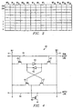
- Fig. 4 shows a detailed diagram of a CAM cell 40 in accordance with the present invention.
- the CAM cell 40 includes a bit storage circuit which is operable to store one bit of one data word.
- the bit storage circuit is comprised of a pair of inverters 43 forming a flip-flop, the upper inverter's output determining memory output.
- Each inverter 43 has an input which is coupled to the other's output and to a pair of bit lines 41 by a corresponding normally-open transistor switch 105 which is controlled by a gate coupled to a row select line 44.
- bit and its complement are set on the bit lines 41, and a logical ⁇ 1' signal is placed on the row select line 44 to close the switches 45.
- the CAM cell 40 also includes a bit compare circuit which is operable to perform a comparison of the bit stored in the CAM cell 40 with a corresponding bit of a target data word, i.e., during a data match operation.
- the bit compare circuit is comprised of a three transistor comparator formed by transistors switches 47 and 49. Each switch 47 is controlled by a gate coupled to the output of a corresponding inverter 43 and a source coupled to a corresponding row select line 41. Switch 49 couples the switches 47 to the match line 46 and to ground.
- the match line 46 is initially pre-charged to logical ⁇ 1' or HIGH.
- the target data bit and its complement are set on the bit lines 41 of the CAM cell 40.
- the bit compare circuit generates a cell output signal which indicates the result of the comparison. If there is a mismatch between the bit stored in the CAM cell 40 and the target data bit, the cell output signal causes the match line 46 to discharged to ground through switch 49. Otherwise, the bit compare circuit of that CAM cell 40 has no effect on the charge of the match line 46.
- All of the CAM cells 40 on the same row in the CAM array 52 share a common match line 46 and thus, during a match operation, the bit lines 41 apply all of the bits of the target data word in parallel to the selectively enabled CAM cells 40 in each row of the CAM array 52. If any enabled CAM cell 40 has a mismatch, it discharges that row's match line 46 to ground. If, however, all of the bits of the enabled CAM cells 40 on a row match their corresponding bit in the target data word, the match line 46 for that row remains at logical ⁇ 1' or HIGH.
- all of the CAM cells 40 in one column in the CAM array 52 share a common pair of bit lines 41.
- Each of the bit line pairs connects a column of CAM cells and provides each bit of the data word and its inverse to selected columns of CAM cells in the CAM array 52 for storage during the data write operation and provides the corresponding bit of the target data word and its inverse to selected columns of CAM cells for comparison during the match operation and accepts the bits of a stored data word retrieved as a result of the data read operation.
- the bit lines 41 simultaneously apply each of the bits of a target data word in parallel to the selectively enabled CAM cells 40 of all rows. Any CAM cell in a row having a mismatch discharges its corresponding matchline 46 to logical ⁇ 0' or LOW, but a row having all matching CAM cells 40 maintains its match line 46 at logical ⁇ 1' or HIGH.
- the output of the OR gate provides a global match indicator signal, not shown, is provided for the CAM array 52.
- the CAM system 50 of the present invention uses four cycles to perform the match operation.
- a first cycle is indicated when the 'column address in' signal has a value of ⁇ 00'.
- a second cycle is indicated when the ⁇ column address in' signal has a value of ⁇ 01'.
- a third cycle is indicated when the 'column address in' signal has a value of ⁇ 10'.
- a fourth cycle is indicated when the 'column address in' signal has a value of ⁇ 11'.
- the CAM controller simultaneously activates the CAM cells corresponding to data word 0 on each row.
- the bit line controller 54 simultaneously activates the CAM cells corresponding to data word 1 on each row.
- bit line controller 54 simultaneously activates the CAM cells corresponding to data word 2 on each row.
- the bit line controller 54 simultaneously activates the CAM cells corresponding to data word 3 on each row.
- At least four cycles are required during the match operation to ensure either finding the target data word or determining that the target data word is not present in the CAM array 52 in that the bit line controller 54 is time multiplexed to provide the target data to only one of the four data words on each row during each cycle.
- only one of the four possible bit line pairs for each bit position (since four interleaved data words are stored on each row in the CAM array 52) is active during any one match cycle.
- the other three pairs of bit lines (which represent the same bit for the other three data words on the same row) are held LOW, at ⁇ 00'. With both bit lines in the bit line pair (BIT and BIT ) held LOW, the compare circuit in the CAM cell does not operate and thus will not cause the match line to discharge.
- the four cycles are thus required to sequentially allow each of the four bit line pairs corresponding to a bit position of each of the four data words stored on a single row to be active while the others are inactive.
- the bit line controller 54 is operable to supply the target data word to more than one of the data words on each row during each cycle.
- the mux factor is not the same as the mux factor in the first embodiment of the present invention.
- the bit line controller 54 is operable to use some property of the target data word, e.g., the least significant bit or any other bit or the parity of any combination of bits, to determine in which of the data words on the selected row to store the data. If, for example, the parity of the least significant bit is used, then even data could be stored in data word 0 or in data word 1 and odd data could be stored in data word 2 or in data word 3. Thus, only two cycles are required to locate the data during a match operation. If the target data is even, data word 0 is searched during the first cycle and data word 1 is searched in the second cycle. If the target data is odd, then data word 2 is searched in the first cycle and data word 3 is searched during the second cycle.
- some property of the target data word e.g., the least significant bit or any other bit or the parity of any combination of bits
- bit line controller 54 uses two bits of the data to determine in which data word on a selected row to store the data during the data write operation, then only one cycle is needed to search for data during the match operation.
- the two least significant bits of the data are used to determine in which data word to store the data, then if the two least significant bits of the data are ⁇ 00', the data is stored in data word 0, if the two least significant bits of the data are ⁇ 01', the data is stored in data word 1, if the two least significant bits of the data are ⁇ 10', the data is stored in data word 2, and if the two least significant bits of the data are ⁇ 11', the data is stored in data word 3.
- the two least significant bits in the target data are used to determine which data word on each row to search in the CAM array 52. Thus, only one lookup cycle is required to search for the target data in the CAM array 52.
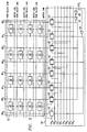
- Fig. 5 is a block diagram illustrating in more detail the control flow between the CAM array 52 and the bit line controller 54.
- Fig. 5 shows four columns and four rows of the CAM array 52.
- Fig. 5 shows the CAM cells 40 for bit 0 of the four data words stored on each of four rows in the CAM array 52. Bits 1-55 of the four data words, not shown, would be similarly structured for each row.
- bit line controller 54 Also shown in Fig. 5 is a detailed portion of the bit line controller 54. Included in the bit line controller 54 is a number of CMOS transmission gates 62, each of which couples each bit D n and its complement D n of a target data word to bit n and its complement n , respectively, of each data word stored on a row of the CAM array 52. In Fig. 5, D 0 and D 0 , generated using inverter 68, are shown connected to their respective CMOS transmission gates 62 through sense amps 64.
- Each of the CMOS transmission gates 62 shown in Fig. 5 are comprised of parallel n-channel and p-channel CMOS transistors.
- the n-channel side of each of the CMOS transmission gates 62 is connected to an enable signal, EN.
- the p-channel side of each of the CMOS transistors 62 is connected to the complement of the associated enable signal, EN .
- there are four enable signals, EN 0 , EN 1 , EN 2 , and EN 3 each of which corresponds to a particular data word.
- the bit line controller 54 sets enable signal EN 0 to logical ⁇ 1', or HIGH which activates all bit positions of data word 0 (W0 0 through W0 55 ), while the other three enable signals, EN 1 , EN 2 , and EN 3 , are set to logical ⁇ 0' or LOW.
- the column address signals are generated by the bit line controller 54 using the selected property.
- bit lines which provide exemplary data bit D 0 of the target data word can be located closely with the same bit of all the data words stored in the CAM array 52, even though multiple data words are stored on each row.
Landscapes
- Dram (AREA)
- Static Random-Access Memory (AREA)
Applications Claiming Priority (2)
| Application Number | Priority Date | Filing Date | Title |
|---|---|---|---|
| US7494998P | 1998-02-17 | 1998-02-17 | |
| US74949P | 1998-02-17 |
Publications (2)
| Publication Number | Publication Date |
|---|---|
| EP0936625A2 true EP0936625A2 (de) | 1999-08-18 |
| EP0936625A3 EP0936625A3 (de) | 2003-09-03 |
Family
ID=22122616
Family Applications (1)
| Application Number | Title | Priority Date | Filing Date |
|---|---|---|---|
| EP99200438A Withdrawn EP0936625A3 (de) | 1998-02-17 | 1999-02-12 | Assoziativspeicher (CAM) |
Country Status (3)
| Country | Link |
|---|---|
| US (1) | US6374325B1 (de) |
| EP (1) | EP0936625A3 (de) |
| JP (1) | JPH11273365A (de) |
Families Citing this family (26)
| Publication number | Priority date | Publication date | Assignee | Title |
|---|---|---|---|---|
| US6505271B1 (en) * | 1999-11-12 | 2003-01-07 | Integrated Device Technology, Inc. | Increasing priority encoder speed using the most significant bit of a priority address |
| US6792502B1 (en) * | 2000-10-12 | 2004-09-14 | Freescale Semiconductor, Inc. | Microprocessor having a content addressable memory (CAM) device as a functional unit therein and method of operation |
| US6700827B2 (en) | 2001-02-08 | 2004-03-02 | Integrated Device Technology, Inc. | Cam circuit with error correction |
| US7017089B1 (en) * | 2001-11-01 | 2006-03-21 | Netlogic Microsystems, Inc | Method and apparatus for testing a content addressable memory device |
| US7076602B2 (en) * | 2001-11-05 | 2006-07-11 | Hywire Ltd. | Multi-dimensional associative search engine having an external memory |
| US7054994B2 (en) * | 2002-07-29 | 2006-05-30 | Hy Wire Ltd. | Multiple-RAM CAM device and method therefor |
| AU2002214240A1 (en) * | 2001-11-05 | 2003-06-10 | Hywire Ltd. | Ram-based range content addressable memory |
| US7401180B1 (en) * | 2001-12-27 | 2008-07-15 | Netlogic Microsystems, Inc. | Content addressable memory (CAM) device having selectable access and method therefor |
| US7117300B1 (en) | 2001-12-27 | 2006-10-03 | James David V | Method and apparatus for restricted search operation in content addressable memory (CAM) devices |
| US7301961B1 (en) | 2001-12-27 | 2007-11-27 | Cypress Semiconductor Corportion | Method and apparatus for configuring signal lines according to idle codes |
| US6728153B2 (en) * | 2002-08-19 | 2004-04-27 | Hewlett-Packard Development Company, L.P. | Magnetic memory which compares first memory cell data bits and second data bits |
| US6934797B2 (en) * | 2002-12-30 | 2005-08-23 | Micron Technology, Inc. | Counter in CAM word |
| US6900999B1 (en) | 2003-06-30 | 2005-05-31 | Integrated Device Technology, Inc. | Ternary content addressable memory (TCAM) cells with small footprint size and efficient layout aspect ratio |
| US6987684B1 (en) | 2003-07-15 | 2006-01-17 | Integrated Device Technology, Inc. | Content addressable memory (CAM) devices having multi-block error detection logic and entry selective error correction logic therein |
| US6870749B1 (en) | 2003-07-15 | 2005-03-22 | Integrated Device Technology, Inc. | Content addressable memory (CAM) devices with dual-function check bit cells that support column redundancy and check bit cells with reduced susceptibility to soft errors |
| US7193876B1 (en) | 2003-07-15 | 2007-03-20 | Kee Park | Content addressable memory (CAM) arrays having memory cells therein with different susceptibilities to soft errors |
| US7304875B1 (en) | 2003-12-17 | 2007-12-04 | Integrated Device Technology. Inc. | Content addressable memory (CAM) devices that support background BIST and BISR operations and methods of operating same |
| US7149101B1 (en) | 2004-12-15 | 2006-12-12 | Netlogic Microsystems, Inc. | Method and apparatus for smoothing current transients in a content addressable memory (CAM) device with dummy searches |
| US8625320B1 (en) | 2010-08-31 | 2014-01-07 | Netlogic Microsystems, Inc. | Quaternary content addressable memory cell having one transistor pull-down stack |
| US8462532B1 (en) | 2010-08-31 | 2013-06-11 | Netlogic Microsystems, Inc. | Fast quaternary content addressable memory cell |
| US8553441B1 (en) | 2010-08-31 | 2013-10-08 | Netlogic Microsystems, Inc. | Ternary content addressable memory cell having two transistor pull-down stack |
| US8582338B1 (en) | 2010-08-31 | 2013-11-12 | Netlogic Microsystems, Inc. | Ternary content addressable memory cell having single transistor pull-down stack |
| US8773880B2 (en) | 2011-06-23 | 2014-07-08 | Netlogic Microsystems, Inc. | Content addressable memory array having virtual ground nodes |
| US8837188B1 (en) | 2011-06-23 | 2014-09-16 | Netlogic Microsystems, Inc. | Content addressable memory row having virtual ground and charge sharing |
| US9001545B2 (en) | 2012-08-31 | 2015-04-07 | Aplus Flash Technology, Inc. | NOR-based BCAM/TCAM cell and array with NAND scalability |
| US20160350012A1 (en) * | 2014-03-20 | 2016-12-01 | Hewlett Packard Enterprise Development Lp | Data source and destination timestamps |
Family Cites Families (12)
| Publication number | Priority date | Publication date | Assignee | Title |
|---|---|---|---|---|
| US4928260A (en) | 1988-05-11 | 1990-05-22 | Advanced Micro Devices, Inc. | Content addressable memory array with priority encoder |
| US4888731A (en) | 1988-05-11 | 1989-12-19 | Advanced Micro Devices, Inc. | Content addressable memory array system with multiplexed status and command information |
| JPH03160694A (ja) * | 1989-11-16 | 1991-07-10 | Mitsubishi Electric Corp | 半導体記憶装置 |
| JP2966638B2 (ja) * | 1992-04-17 | 1999-10-25 | 三菱電機株式会社 | ダイナミック型連想メモリ装置 |
| JP2775549B2 (ja) * | 1992-05-08 | 1998-07-16 | 三菱電機株式会社 | 連想メモリセルおよび連想メモリ回路 |
| US5383146A (en) | 1992-06-08 | 1995-01-17 | Music Semiconductors, Inc. | Memory with CAM and RAM partitions |
| JPH0676583A (ja) | 1992-07-06 | 1994-03-18 | Mitsubishi Electric Corp | 内容番地付記憶装置および一致ワード不要化方法 |
| US5642322A (en) * | 1995-05-24 | 1997-06-24 | Kawasaki Steel Corporation | Layout of semiconductor memory and content-addressable memory |
| JP3038649B2 (ja) * | 1997-04-16 | 2000-05-08 | 日本電気株式会社 | 連想検索装置および方法 |
| JP3036467B2 (ja) * | 1997-06-19 | 2000-04-24 | 日本電気株式会社 | 最長一致検出装置 |
| US5943252A (en) * | 1997-09-04 | 1999-08-24 | Northern Telecom Limited | Content addressable memory |
| US6101116A (en) * | 1999-06-30 | 2000-08-08 | Integrated Device Technology, Inc. | Six transistor content addressable memory cell |
-
1999
- 1999-02-12 EP EP99200438A patent/EP0936625A3/de not_active Withdrawn
- 1999-02-17 JP JP11038899A patent/JPH11273365A/ja active Pending
- 1999-02-17 US US09/251,517 patent/US6374325B1/en not_active Expired - Lifetime
Also Published As
| Publication number | Publication date |
|---|---|
| JPH11273365A (ja) | 1999-10-08 |
| US6374325B1 (en) | 2002-04-16 |
| EP0936625A3 (de) | 2003-09-03 |
Similar Documents
| Publication | Publication Date | Title |
|---|---|---|
| US6374325B1 (en) | Content addressable memory (CAM) | |
| US5752260A (en) | High-speed, multiple-port, interleaved cache with arbitration of multiple access addresses | |
| US7502245B2 (en) | Content addressable memory architecture | |
| US5014195A (en) | Configurable set associative cache with decoded data element enable lines | |
| US9076527B2 (en) | Charge sharing in a TCAM array | |
| US5343437A (en) | Memory having nonvolatile and volatile memory banks | |
| US5267210A (en) | SRAM with flash clear for selectable I/OS | |
| US20070074070A1 (en) | Repairable block redundancy scheme | |
| US5668972A (en) | Method and system for efficient miss sequence cache line allocation utilizing an allocation control cell state to enable a selected match line | |
| US5657291A (en) | Multiport register file memory cell configuration for read operation | |
| US20090141527A1 (en) | Apparatus and method for implementing matrix-based search capability in content addressable memory devices | |
| US6525987B2 (en) | Dynamically configured storage array utilizing a split-decoder | |
| US5367655A (en) | Memory and associated method including an operating mode for simultaneously selecting multiple rows of cells | |
| US6571323B2 (en) | Memory-access management method and system for synchronous dynamic Random-Access memory or the like | |
| HK1003851B (en) | A memory apparatus and method for use in a data processing system | |
| US5890221A (en) | Method and system for offset miss sequence handling in a data cache array having multiple content addressable field per cache line utilizing an MRU bit | |
| US6707752B2 (en) | Tag design for cache access with redundant-form address | |
| GB2244157A (en) | Apparatus for row caching in random access memory | |
| KR20080009129A (ko) | 저장 회로 및 방법 | |
| JP2777034B2 (ja) | 半導体記憶装置 | |
| JP2754492B2 (ja) | 選択的にクリア可能なメモリセルを備えたメモリ | |
| KR910010136B1 (ko) | Lru 회로 | |
| JPH06105557B2 (ja) | 連想メモリ装置 | |
| KR19980035680A (ko) | 어드레스 변환기 회로 | |
| JPH04271087A (ja) | 半導体記憶装置 |
Legal Events
| Date | Code | Title | Description |
|---|---|---|---|
| PUAI | Public reference made under article 153(3) epc to a published international application that has entered the european phase |
Free format text: ORIGINAL CODE: 0009012 |
|
| AK | Designated contracting states |
Kind code of ref document: A2 Designated state(s): AT BE CH CY DE DK ES FI FR GB GR IE IT LI LU MC NL PT SE |
|
| AX | Request for extension of the european patent |
Free format text: AL;LT;LV;MK;RO;SI |
|
| PUAL | Search report despatched |
Free format text: ORIGINAL CODE: 0009013 |
|
| AK | Designated contracting states |
Kind code of ref document: A3 Designated state(s): AT BE CH CY DE DK ES FI FR GB GR IE IT LI LU MC NL PT SE |
|
| AX | Request for extension of the european patent |
Extension state: AL LT LV MK RO SI |
|
| RIC1 | Information provided on ipc code assigned before grant |
Ipc: 7G 11C 15/04 B Ipc: 7G 11C 15/00 A |
|
| 17P | Request for examination filed |
Effective date: 20040303 |
|
| AKX | Designation fees paid |
Designated state(s): DE FR GB |
|
| 17Q | First examination report despatched |
Effective date: 20040429 |
|
| STAA | Information on the status of an ep patent application or granted ep patent |
Free format text: STATUS: THE APPLICATION IS DEEMED TO BE WITHDRAWN |
|
| 18D | Application deemed to be withdrawn |
Effective date: 20041110 |