EP0936679A1 - Procédé pour fabriquer des dispositifs semi-conducteurs avec condensateur intégré - Google Patents
Procédé pour fabriquer des dispositifs semi-conducteurs avec condensateur intégré Download PDFInfo
- Publication number
- EP0936679A1 EP0936679A1 EP99103398A EP99103398A EP0936679A1 EP 0936679 A1 EP0936679 A1 EP 0936679A1 EP 99103398 A EP99103398 A EP 99103398A EP 99103398 A EP99103398 A EP 99103398A EP 0936679 A1 EP0936679 A1 EP 0936679A1
- Authority
- EP
- European Patent Office
- Prior art keywords
- etching
- platinum
- layer
- gas
- resist
- Prior art date
- Legal status (The legal status is an assumption and is not a legal conclusion. Google has not performed a legal analysis and makes no representation as to the accuracy of the status listed.)
- Granted
Links
- 238000004519 manufacturing process Methods 0.000 title claims abstract description 21
- 239000004065 semiconductor Substances 0.000 title claims abstract description 17
- 239000003990 capacitor Substances 0.000 title abstract description 13
- BASFCYQUMIYNBI-UHFFFAOYSA-N platinum Chemical compound [Pt] BASFCYQUMIYNBI-UHFFFAOYSA-N 0.000 claims abstract description 213
- 229910052697 platinum Inorganic materials 0.000 claims abstract description 102
- VYPSYNLAJGMNEJ-UHFFFAOYSA-N Silicium dioxide Chemical compound O=[Si]=O VYPSYNLAJGMNEJ-UHFFFAOYSA-N 0.000 claims abstract description 33
- 229910052814 silicon oxide Inorganic materials 0.000 claims abstract description 33
- 238000009413 insulation Methods 0.000 claims abstract description 18
- 239000000758 substrate Substances 0.000 claims abstract description 11
- 239000004215 Carbon black (E152) Substances 0.000 claims abstract description 7
- 229930195733 hydrocarbon Natural products 0.000 claims abstract description 7
- 150000002430 hydrocarbons Chemical class 0.000 claims abstract description 7
- HEDRZPFGACZZDS-UHFFFAOYSA-N Chloroform Chemical compound ClC(Cl)Cl HEDRZPFGACZZDS-UHFFFAOYSA-N 0.000 claims description 48
- 229910052751 metal Inorganic materials 0.000 claims description 23
- 239000002184 metal Substances 0.000 claims description 23
- 238000001312 dry etching Methods 0.000 claims description 20
- KDLHZDBZIXYQEI-UHFFFAOYSA-N Palladium Chemical compound [Pd] KDLHZDBZIXYQEI-UHFFFAOYSA-N 0.000 claims description 11
- 229910052763 palladium Inorganic materials 0.000 claims description 5
- 238000005530 etching Methods 0.000 abstract description 178
- XUIMIQQOPSSXEZ-UHFFFAOYSA-N Silicon Chemical compound [Si] XUIMIQQOPSSXEZ-UHFFFAOYSA-N 0.000 abstract description 5
- 239000010703 silicon Substances 0.000 abstract description 5
- 229910052710 silicon Inorganic materials 0.000 abstract description 5
- 230000006866 deterioration Effects 0.000 abstract 1
- 239000010410 layer Substances 0.000 description 107
- 239000007789 gas Substances 0.000 description 86
- 239000010408 film Substances 0.000 description 33
- 239000003989 dielectric material Substances 0.000 description 22
- 238000000034 method Methods 0.000 description 21
- 239000000463 material Substances 0.000 description 12
- 238000001020 plasma etching Methods 0.000 description 7
- 229910052774 Proactinium Inorganic materials 0.000 description 5
- 238000006243 chemical reaction Methods 0.000 description 5
- 238000000992 sputter etching Methods 0.000 description 5
- OKTJSMMVPCPJKN-UHFFFAOYSA-N Carbon Chemical compound [C] OKTJSMMVPCPJKN-UHFFFAOYSA-N 0.000 description 4
- UFHFLCQGNIYNRP-UHFFFAOYSA-N Hydrogen Chemical compound [H][H] UFHFLCQGNIYNRP-UHFFFAOYSA-N 0.000 description 4
- 229910052799 carbon Inorganic materials 0.000 description 4
- 239000001257 hydrogen Substances 0.000 description 4
- 229910052739 hydrogen Inorganic materials 0.000 description 4
- 229910003446 platinum oxide Inorganic materials 0.000 description 4
- 238000012545 processing Methods 0.000 description 4
- QVGXLLKOCUKJST-UHFFFAOYSA-N atomic oxygen Chemical compound [O] QVGXLLKOCUKJST-UHFFFAOYSA-N 0.000 description 3
- 238000007796 conventional method Methods 0.000 description 3
- 230000003247 decreasing effect Effects 0.000 description 3
- 230000000694 effects Effects 0.000 description 3
- 239000001301 oxygen Substances 0.000 description 3
- 229910052760 oxygen Inorganic materials 0.000 description 3
- 238000009877 rendering Methods 0.000 description 3
- 101100496858 Mus musculus Colec12 gene Proteins 0.000 description 2
- QZPSXPBJTPJTSZ-UHFFFAOYSA-N aqua regia Chemical compound Cl.O[N+]([O-])=O QZPSXPBJTPJTSZ-UHFFFAOYSA-N 0.000 description 2
- 230000015572 biosynthetic process Effects 0.000 description 2
- 230000007423 decrease Effects 0.000 description 2
- 238000011161 development Methods 0.000 description 2
- 230000018109 developmental process Effects 0.000 description 2
- 239000011229 interlayer Substances 0.000 description 2
- 229910044991 metal oxide Inorganic materials 0.000 description 2
- 150000004706 metal oxides Chemical class 0.000 description 2
- VZGDMQKNWNREIO-UHFFFAOYSA-N tetrachloromethane Chemical compound ClC(Cl)(Cl)Cl VZGDMQKNWNREIO-UHFFFAOYSA-N 0.000 description 2
- 238000001039 wet etching Methods 0.000 description 2
- 208000032365 Electromagnetic interference Diseases 0.000 description 1
- 238000003486 chemical etching Methods 0.000 description 1
- 150000001875 compounds Chemical class 0.000 description 1
- 239000000470 constituent Substances 0.000 description 1
- 230000002542 deteriorative effect Effects 0.000 description 1
- 238000001125 extrusion Methods 0.000 description 1
- 239000001307 helium Substances 0.000 description 1
- 229910052734 helium Inorganic materials 0.000 description 1
- SWQJXJOGLNCZEY-UHFFFAOYSA-N helium atom Chemical compound [He] SWQJXJOGLNCZEY-UHFFFAOYSA-N 0.000 description 1
- 229910000039 hydrogen halide Inorganic materials 0.000 description 1
- 239000012433 hydrogen halide Substances 0.000 description 1
- 238000012986 modification Methods 0.000 description 1
- 230000004048 modification Effects 0.000 description 1
- 238000000206 photolithography Methods 0.000 description 1
- 239000010970 precious metal Substances 0.000 description 1
- 230000005855 radiation Effects 0.000 description 1
- 238000012827 research and development Methods 0.000 description 1
- 238000004528 spin coating Methods 0.000 description 1
- 239000010409 thin film Substances 0.000 description 1
- 239000003039 volatile agent Substances 0.000 description 1
Images



Classifications
-
- H—ELECTRICITY
- H10—SEMICONDUCTOR DEVICES; ELECTRIC SOLID-STATE DEVICES NOT OTHERWISE PROVIDED FOR
- H10D—INORGANIC ELECTRIC SEMICONDUCTOR DEVICES
- H10D1/00—Resistors, capacitors or inductors
- H10D1/60—Capacitors
- H10D1/68—Capacitors having no potential barriers
Definitions
- This invention relates to a method for manufacturing a semiconductor integrated circuit chip having a built-in capacitor in which high dielectric constant material or ferroelectric material is used as a capacitance insulation layer.
- the high dielectric constant materials or ferroelectric materials are made mainly of sintered metal oxide, and contain a substantial amount of very reactive oxygen.
- material for its electrodes must be least reactive; thus, precious metals such as platinum (Pt), palladium (Pd), etc. must be used.
- platinum and palladium etching has been conducted by means of isotropic etching, such as wet etching with aqua regia or by ion milling with Ar gas. Because of the nature of isotropic etching, using wet etching with aqua regia and ion milling causes deteriorated processing accuracy. Furthermore, an additional problem with ion milling occurs because the etching speed on platinum, which is to form the electrode, and on silicon oxide, etc., which is underneath the platinum, are almost the same, the silicon oxide is also etched during ion milling.
- a silicon oxide layer 4 is formed as an insulation layer on top of a circuit element 1 and a wiring 2 shaped on a silicon substrate 3.
- a first platinum layer 5 is formed over the silicon oxide layer 4 and a film of high dielectric constant material or ferroelectric material (hereinafter referred to as dielectric film) 6 and a second platinum layer 7.
- the silicon oxide layer 4 reflects unevenness due to the circuit element 1 or wiring 2 already shaped on the silicon substrate 3 to have a hollow 8 or protrusion 9 on its surface, as shown in FIG. 8(a). Because dielectric film 6 is spin-coated on the uneven surface of silicon oxide layer 4, thickness of the dielectric film 6 is large at the hollow 8, and small at the protrusion 9.
- top electrode 7a and capacitance insulation film 6a are formed by dry-etching the second platinum layer 7 and dielectric film 6 with Cl 2 , HBr as the etching gas.
- the facility used for the etching is a magnetron reactive ion etching (RIE) mode. dry etcher.
- RIE magnetron reactive ion etching
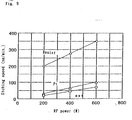
- FIG. 9 shows dependence of the etching speed of platinum, BST and resist to RF power.
- the horizontal axis denotes RF power
- the vertical axis denotes etching speeds of platinum, BST and resist.
- the facility used for the etching is magnetron RIE mode dry etcher.
- the etcher conditions are: Cl 2 gas flow 20 sccm, gas pressure 1 Pa, RF power within a range between 200W and 600W, wafer temperature during etching below 20°C as its back surface is cooled with He.
- FIG. 9 exhibits that platinum etching speed is increased from 30 nm/min. to 100 nm/min., BST etching speed is increased from 20 nm/min. to 70 nm/min. and resist etching speed is increased from 200 nm/min. to 350 nm/min., when RF power is raised from 200W to 600W.
- the platinum/resist etching speed ratio increases from about 0.15 to about 0.29 along with the increase of RF power from 200W to 600W.
- the BST/resist etching speed ratio also increases from about 0.10 to about 0.20. Under any condition, the etching speed of resist is much faster than that of platinum and BST.
- the time required to etch the platinum layer (200nm thick) and BST (200nm thick) with RF power at 600W is 4 min. 52 sec.
- the etching quantity of the resist during this time span is calculated from the resist etching speed to be 1703nm, a very large value. This means that, if the resist layer is thinner than 1700nm, the resist is entirely etched while etching is conducted on the platinum and BST. If this is to be prevented, a thick resist layer of more than about 3 ⁇ m thick has to be used.
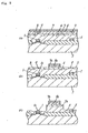
- the etching speed of the silicon oxide layer is about 2.5 times faster than that of the platinum layer. So, as shown in FIG. 8(c), during formation of bottom electrode 5a, its underlayer, the silicon oxide layer 4 is significantly etched.
- FIGs. 8(b) and 8(c) The problem with etching the silicon oxide layer 4 is illustrated in FIGs. 8(b) and 8(c).
- the etching gas which already etched the thin part of first platinum layer 5 (located on the extrusion 9 of silicon oxide layer 4), quickly attacks the underlying silicon oxide layer 4 to etch it off, and when gate electrode 1a of circuit element 1 and wiring 2 are exposed, they are also etched, rendering the transistor and other circuit element 1 inoperable.
- the objective of this invention is to offer a new method for manufacturing semiconductor devices having a built-in capacitor which is formed by slowing the etching speed on the resist, making the ratio of etching speed of platinum and dielectric material to resist large, and by selectively dry-etching the platinum and dielectric material at a fast etching speed.
- Another objective of this invention is to offer a new method of manufacturing semiconductor devices, wherein, even if sufficient time is provided for overetching during the process to form the bottom electrode of the capacitor, the silicon oxide layer underneath the electrode is only minimally etched, hence circuit elements and wirings, etc. are protected from damage; thereby highly reliable semiconductor devices can be manufactured.
- This invention comprises process steps to form, on a substrate in which circuit elements and wirings, etc. are already shaped, an insulation layer, a first metal layer, a dielectric film and a second metal layer, one after another, and then, form a top electrode and a capacitance film by dry etching the second metal layer and the dielectric film, and form a bottom electrode by,dry etching the first metal layer; wherein, at least the etching gas for dry etching the second metal layer is a gas containing hydrocarbon such as chloroform.
- This invention employs a silicon oxide layer as the insulation layer on the substrate, and a platinum layer or palladium layer as the first and second metal layers. Dry etching of the second metal layer and dielectric film is conducted in a low pressure region not higher than about 5 Pa, where the etching speed is high.
- an insulation layer, a first metal layer, a dielectric film and a second metal layer are formed on a substrate on which circuit elements and wirings, etc. are already shaped; and then a top electrode and a capacitance insulation layer are formed by dry etching the second metal layer and dielectric film in the low pressure region where the etching speed is high.
- the dielectric film left unetched on the first metal layer is removed under the high pressure region where the etching speed relative to the first metal layer is low, and then the mask pattern is applied, and the bottom electrode is formed by dry etching the first metal layer under the low pressure region where the etching speed is high.
- etching of the platinum and dielectric material may be conducted by using a mask of normal layer-thickness resist (generally speaking, about 1.2 ⁇ m to about 2.0 ⁇ m thick), instead of using a conventional thick-layer resist (about 3 ⁇ m and thicker).
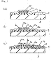
- an insulation layer 4 of silicon oxide, etc. is formed on the substrate 3 made of silicon, etc.
- a first platinum layer 5 of about 200nm thickness.
- a dielectric film 6 having a high dielectric constant material or ferroelectric material of about 200nm thickness.
- a second platinum layer 7 of about 200nm thickness.
- the dielectric film 6 is formed by means of the spin coating method.
- top electrode 7a and a capacitance insulation film 6a are formed by dry etching the second platinum layer 7 and dielectric film 6, through a resist layer 10 applied on the second platinum layer 7. In this way, a device as shown in FIG.
- FIG. 1(b) is formed.
- the top electrode 7a, capacitance insulation film 6a and a part of the first platinum layer 5 are covered with a second resist layer 11 to etch the first platinum layer 5 with a mixed gas of HBr and O 2 .
- Bottom electrode 5a is thus formed, as shown in FIG. 1(d).
- an interlayer insulation layer 12 is coated over the entire surface, contact holes 13a and 13b are provided above the bottom electrode 5a and top electrode 7a, respectively (Fig. 2(b)), and electrode wirings 14a and 14b, which connect to the top electrode 7a and bottom electrode 5a, respectively, via the contact holes 13b, 13a, are formed to complete a capacitor (FIG. 2(c)).
- FIG. 3 shows the etching speeds of platinum and silicon oxide when HBr and O 2 mixed gas is used.
- the left vertical axis denotes the etching speeds of platinum and silicon oxide
- the right vertical axis denotes the etching selectivity ratio (platinum etching speed/silicon oxide etching speed)
- the horizontal axis indicates percentage of O 2 flow to the HBr and O 2 total etching gas flow.
- the etching facility used is a magnetron RIE mode dry etcher, with HF power 400W and pressure 1.33P during etching.
- the etching speed on silicon oxide when HBr alone is used as the etching gas is about 80 nm/min., which is about half the speed when chloroform is used as the etching gas, or almost the same level as that on platinum (90 nm/min.). Namely, the platinum/silicon oxide etching selectivity ratio is improved to approximately 1.
- the speed of etching on silicon oxide decreases to about 1/3 as compared with the case of HBr alone; while the etching speed on platinum stays almost unchanged.
- the platinum/silicon oxide etching selectivity ratio is improved to more than 3.
- the quantity of O 2 to the total etching gas flow may be chosen from the range of about 10%-35%.
- the silicon oxide reacts with Br and O 2 to compose a non-volatile compound which piles up on the silicon oxide layer 4 to protect the silicon oxide layer 4, lowering the etching speed.
- the sane effect is also obtained by the use of a less reactive metal, such as palladium.
- a compound gas containing oxygen may also be used.
- the etching gas for forming the bottom electrode 5a made of platinum, etc. only the first metal layer 5 made of platinum, etc. is selectively etched off, and etching on the silicon oxide layer 4 is suppressed; therefore the circuit elements and wiring, etc. underneath the silicon oxide layer are not damaged.
- the method for manufacturing semiconductor devices of the invention is the same as that shown in FIGs. 1(a)-(d) and FIGs. 2(a)-(c), except that chloroform is used as the etching gas on the platinum and dielectric material.
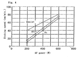
- FIG. 4 shows the dependence of etching speeds of platinum, BST and resist to HF power when chloroform (CHCl 3 ) is used as the etching gas.
- the horizontal axis denotes HF power
- the vertical axis etching speeds of platinum, BST and resist The etching facility used is a magnetron RIE mode dry etcher.
- the etching conditions are as follows: chloroform (CHCl 3 ) flow 20 sccm, gas pressure 1 Pa, and HF power within a range of about 200W-600W.
- FIG. 4 indicates, along with the elevation of HF power from about 200W to about 600W the speed of etching on platinum increases from about 10 nm/min to about 70 nm/min, on BTS from about 15 nm/min to about 75 nm/min, and on resist from 40 nm/min to 80 nm/min.
- Platinum/resist etching speed ratio increases from about 0.25 to about 0.88 when HF power is raised from about 200W to about 600W.
- BST/resist etching speed ratio increase from about 0.38 to about 0.94.
- the time needed to etch platinum (200nm thick layer) and BST (200nm thick film) is 5 min. 32 sec. at HF power load 600W. During that time frame, the resist is calculated to have been etched off by 443nm; which represents a remarkable improvement as compared with the conventional etching quantity 1703nm.
- the etching speed of the resist is decreased because of the carbon and hydrogen contained in the chloroform gas. It is believed that either the reaction with carbon and hydrogen in the resist is made less active, or a film of carbon and hydrogen is polymerized during etching which piles up on the resist while etching is going on, rendering the etching speed retarded.
- chloroform (CHCl 3 ) is used as an example of the etching gas.
- other gases containing hydrocarbon may be used to obtain the sane results.
- a mixed gas of Cl 2 gas and chloroform, and a mixed gas of HBr and chloroform may also be used to obtain the same results.
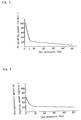
- the horizontal axis denotes gas pressure and the vertical axis speed of etching on platinum.
- the etching facility used is a magnetron RIE mode dry etcher.
- the etching conditions are as follows: etching gas flow 20 sccm and HF power 600W.
- the substrate temperature during etching is below about 20°C because its back surface is cooled with helium (He).
- the speed of etching on platinum increases rapidly from about 30 nm/min to about 100 nm/min when the gas pressure decreases from about 5 Pa to about 1 Pa. Meanwhile, when the gas pressure is increased from about 5 Pa to about 50 Pa, the etching speed slows down from less than about 30 nm/min to about 5 nm/min.
- the physical spatter etching dominates, and the etching speed increases steeply along with the lowering pressure.
- the physical spatter etching is weak, and etching by the chemical reaction with platinum and etching gas seems to be proceeding, where the etching speed is very slow.
- the speed of etching on platinum during platinum etching can be increased steeply by conducting the etching in the low pressure region, about 1 Pa-5 Pa.
- FIG. 6 shows the dependence of the etching speed of the dielectric material on the gas pressure when a mixed gas of Cl 2 gas and chloroform is used as etching gas.
- the horizontal axis denotes the gas pressure and the vertical axis denotes the etching speed on the dielectric material.
- the dielectric material used as an example is BaSrTio 3 (BST).
- the etching facility used is a magnetron RIE mode dry etcher.
- the etching conditions are as follows: etching gas flow 20 sccm and HF power 600W.
- the substrate temperature during etching is below 20°C because its back surface is cooled with He.
- the etching speed on the dielectric material increases from about 30 nm/min to about 60 nm/min along with the decreasing gas pressure from about 5 Pa to about 1 Pa. Meanwhile, when the gas pressure goes higher (from about 5 Pa to about 50 Pa), the etching speed gradually slows down (from about 30 nm/min to about 15 nm/min).
- the physical spatter etching dominates, and the etching speed increases steeply along with the lowering pressure.
- the physical spatter etching is weak, and etching by the chemical reaction with the dielectric material and etching gas occurs.
- FIG. 7 shows the dependence of the intensity of light emitted during etching of the dielectric material to the gas pressure.
- the etching conditions remain the same as those in FIG. 6, and the horizontal axis denotes the gas pressure and vertical axis the intensity of light emitted.
- the etching speed can be increased by setting the etching conditions within the 1-5 Pa low pressure region. Thus, there is an improved production throughout.
- the etching speed can be increased steeply by performing the etching in the 1-5 Pa low pressure region, and the etching by chemical reaction can be performed in the 5-50 Pa high pressure region.
- the first platinum layer 5 of 200nm thickness is formed as a bottom electrode, on the first platinum layer 5 the dielectric film 6 is formed of 180 nm thickness, and then on the dielectric film 6 the second platinum layer 7 of 200 nm thickness is formed for a top electrode.
- the first resist layer 10 is then applied on the second platinum layer 7 to etch down the second platinum layer 7 and the dielectric film 6.
- the etching is discontinued.
- the ratio of etching speed of the dielectric film 6 to the first platinum layer 5 underneath the film 6 needs to be high.
- the second resist layer 11 is applied to etch off the first platinum layer 5, in order to form the bottom electrode 5a.
- the size of the first platinum layer 5 needs to be large enough to provide contacts through the interlayer insulation layer 12 at two points between the second platinum layer 7/the first platinum layer 5 and electrode wirings 14a/14b, which are located above the respective platinum layers.
- the second platinum layer 7 must be etched in the low pressure region, where the speed of etching on platinum is high.
- the etching conditions in this process are: etching gas flow 20 sccm, gas pressure 1 Pa, HF power 600W and etching time 2 minutes.
- the etching conditions should be: etching gas flow 20 sccm, gas pressure 1 Pa, HF power 600W and etching time 3 minutes.
- the etching conditions at this process are: etching gas flow 20 sccm, gas pressure 50 Pa, HF power 600W and etching time 1 min.
- the ratio of etching speed of the dielectric material to platinum increases from about 0.6 to about 3, along with the increasing gas pressure from about 1 Pa to about 50 Pa.
- platinum and dielectric material can be selectively etched by shifting the pressure region of the etching gas.
- the first platinum layer 5 is etched in the low pressure region, where platinum etching speed is high.
- the etching conditions at this step are: etching gas flow 20 sccm, gas pressure 1 Pa, HT power 600W and etching time 2 minutes.
- a mixed gas of Cl 2 gas and chloroform is used as an example of etching gas.
- Cl 2 gas alone may be used as etching gas, and the same effects may be obtained by controlling the pressure region during the dry etching process in the same way as described in embodiments 3 and 4 above.
- a desirable etching speed may be chosen to fit each platinum and dielectric material. Also a required ratio of the etching speed of platinum to dielectric material may be chosen by properly controlling the pressure region of the etching gas.
- a capacitor consisting of the second platinum layer 7 as top electrode, dielectric film 6 and the first platinum layer 5 as bottom electrode may be formed with high precision and without difficulty of manufacturing.
Landscapes
- Drying Of Semiconductors (AREA)
- Semiconductor Memories (AREA)
- Semiconductor Integrated Circuits (AREA)
Applications Claiming Priority (5)
| Application Number | Priority Date | Filing Date | Title |
|---|---|---|---|
| JP6088394 | 1994-03-30 | ||
| JP6088394 | 1994-03-30 | ||
| JP8668694 | 1994-04-25 | ||
| JP8668694 | 1994-04-25 | ||
| EP95104614A EP0675548B1 (fr) | 1994-03-30 | 1995-03-29 | Procédé pour fabriquer des dispositifs semi-conducteurs avec condensateur intégré |
Related Parent Applications (1)
| Application Number | Title | Priority Date | Filing Date |
|---|---|---|---|
| EP95104614A Division EP0675548B1 (fr) | 1994-03-30 | 1995-03-29 | Procédé pour fabriquer des dispositifs semi-conducteurs avec condensateur intégré |
Publications (2)
| Publication Number | Publication Date |
|---|---|
| EP0936679A1 true EP0936679A1 (fr) | 1999-08-18 |
| EP0936679B1 EP0936679B1 (fr) | 2002-11-27 |
Family
ID=26401935
Family Applications (2)
| Application Number | Title | Priority Date | Filing Date |
|---|---|---|---|
| EP99103398A Expired - Lifetime EP0936679B1 (fr) | 1994-03-30 | 1995-03-29 | Procédé pour fabriquer des dispositifs semi-conducteurs avec condensateur intégré |
| EP95104614A Expired - Lifetime EP0675548B1 (fr) | 1994-03-30 | 1995-03-29 | Procédé pour fabriquer des dispositifs semi-conducteurs avec condensateur intégré |
Family Applications After (1)
| Application Number | Title | Priority Date | Filing Date |
|---|---|---|---|
| EP95104614A Expired - Lifetime EP0675548B1 (fr) | 1994-03-30 | 1995-03-29 | Procédé pour fabriquer des dispositifs semi-conducteurs avec condensateur intégré |
Country Status (3)
| Country | Link |
|---|---|
| EP (2) | EP0936679B1 (fr) |
| DE (2) | DE69529000T2 (fr) |
| MY (1) | MY130503A (fr) |
Families Citing this family (4)
| Publication number | Priority date | Publication date | Assignee | Title |
|---|---|---|---|---|
| TW365691B (en) * | 1997-02-05 | 1999-08-01 | Samsung Electronics Co Ltd | Method for etching Pt film of semiconductor device |
| US7100277B2 (en) * | 2004-07-01 | 2006-09-05 | E. I. Du Pont De Nemours And Company | Methods of forming printed circuit boards having embedded thick film capacitors |
| US20060120015A1 (en) | 2004-12-02 | 2006-06-08 | Borland William J | Thick-film capacitors, embedding thick-film capacitors inside printed circuit boards, and methods of forming such capacitors and printed circuit boards |
| KR100769459B1 (ko) | 2005-10-28 | 2007-10-23 | 주식회사 코미코 | 미세 전극을 갖는 세라믹 소자의 제조방법 |
Citations (6)
| Publication number | Priority date | Publication date | Assignee | Title |
|---|---|---|---|---|
| JPS62234331A (ja) * | 1986-04-04 | 1987-10-14 | Hitachi Ltd | アルミニウム合金膜のドライエツチング方法 |
| JPS6376329A (ja) * | 1986-09-19 | 1988-04-06 | Fujitsu Ltd | エツチング方法 |
| EP0295581A1 (fr) * | 1987-06-19 | 1988-12-21 | Tegal Corporation | Procédé de décapage d'aluminium dans un plasma |
| JPS6453548A (en) * | 1987-08-25 | 1989-03-01 | Matsushita Electric Industrial Co Ltd | Dry etching of aluminum-silicon-copper alloy |
| US5094712A (en) * | 1990-10-09 | 1992-03-10 | Micron Technology, Inc. | One chamber in-situ etch process for oxide and conductive material |
| US5397433A (en) * | 1993-08-20 | 1995-03-14 | Vlsi Technology, Inc. | Method and apparatus for patterning a metal layer |
Family Cites Families (2)
| Publication number | Priority date | Publication date | Assignee | Title |
|---|---|---|---|---|
| US5258332A (en) * | 1987-08-28 | 1993-11-02 | Kabushiki Kaisha Toshiba | Method of manufacturing semiconductor devices including rounding of corner portions by etching |
| US5254217A (en) * | 1992-07-27 | 1993-10-19 | Motorola, Inc. | Method for fabricating a semiconductor device having a conductive metal oxide |
-
1995
- 1995-03-29 DE DE69529000T patent/DE69529000T2/de not_active Expired - Fee Related
- 1995-03-29 MY MYPI95000791A patent/MY130503A/en unknown
- 1995-03-29 EP EP99103398A patent/EP0936679B1/fr not_active Expired - Lifetime
- 1995-03-29 EP EP95104614A patent/EP0675548B1/fr not_active Expired - Lifetime
- 1995-03-29 DE DE69527669T patent/DE69527669T2/de not_active Expired - Fee Related
Patent Citations (6)
| Publication number | Priority date | Publication date | Assignee | Title |
|---|---|---|---|---|
| JPS62234331A (ja) * | 1986-04-04 | 1987-10-14 | Hitachi Ltd | アルミニウム合金膜のドライエツチング方法 |
| JPS6376329A (ja) * | 1986-09-19 | 1988-04-06 | Fujitsu Ltd | エツチング方法 |
| EP0295581A1 (fr) * | 1987-06-19 | 1988-12-21 | Tegal Corporation | Procédé de décapage d'aluminium dans un plasma |
| JPS6453548A (en) * | 1987-08-25 | 1989-03-01 | Matsushita Electric Industrial Co Ltd | Dry etching of aluminum-silicon-copper alloy |
| US5094712A (en) * | 1990-10-09 | 1992-03-10 | Micron Technology, Inc. | One chamber in-situ etch process for oxide and conductive material |
| US5397433A (en) * | 1993-08-20 | 1995-03-14 | Vlsi Technology, Inc. | Method and apparatus for patterning a metal layer |
Non-Patent Citations (3)
| Title |
|---|
| PATENT ABSTRACTS OF JAPAN vol. 012, no. 106 (E - 596) 6 April 1988 (1988-04-06) * |
| PATENT ABSTRACTS OF JAPAN vol. 012, no. 308 (E - 647) 22 August 1988 (1988-08-22) * |
| PATENT ABSTRACTS OF JAPAN vol. 013, no. 254 (E - 772) 13 June 1989 (1989-06-13) * |
Also Published As
| Publication number | Publication date |
|---|---|
| DE69527669T2 (de) | 2003-02-06 |
| DE69529000T2 (de) | 2003-08-21 |
| DE69527669D1 (de) | 2002-09-12 |
| EP0936679B1 (fr) | 2002-11-27 |
| EP0675548A3 (fr) | 1996-03-13 |
| EP0675548A2 (fr) | 1995-10-04 |
| MY130503A (en) | 2007-06-29 |
| EP0675548B1 (fr) | 2002-08-07 |
| DE69529000D1 (de) | 2003-01-09 |
Similar Documents
| Publication | Publication Date | Title |
|---|---|---|
| US5527729A (en) | Method of manufacturing a capacitor having metal electrodes | |
| KR100480610B1 (ko) | 실리콘 산화막을 이용한 미세 패턴 형성방법 | |
| US20060073614A1 (en) | Ferroelectric capacitor structure and manufacturing method thereof | |
| JPH0817930A (ja) | エッチング・ストップ層を利用する半導体装置構造とその方法 | |
| US8609543B2 (en) | Method for manufacturing semiconductor device having multi-layered hard mask layer | |
| JP2003133414A (ja) | 半導体素子及びその製造方法 | |
| US5856239A (en) | Tungsten silicide/ tungsten polycide anisotropic dry etch process | |
| KR19990065766A (ko) | 반도체장치의 백금막 식각방법 | |
| KR970001203B1 (ko) | 폴리실리콘 막 에칭 방법 | |
| US20020132194A1 (en) | Method and manufacturing a semiconductor device having a ruthenium or a ruthenium oxide | |
| EP0936679B1 (fr) | Procédé pour fabriquer des dispositifs semi-conducteurs avec condensateur intégré | |
| KR20050014440A (ko) | 폴리실리콘 식각 마스크를 이용한 반도체 소자의 제조방법 | |
| JP3700231B2 (ja) | 接続孔の形成方法 | |
| US20040082184A1 (en) | Polysilicon etching method | |
| US6379872B1 (en) | Etching of anti-reflective coatings | |
| US6722376B2 (en) | Polysilicon etch useful during the manufacture of a semiconductor device | |
| US6537906B1 (en) | Methods for fabricating semiconductor devices | |
| KR100703025B1 (ko) | 반도체 장치에서 금속 배선 형성 방법. | |
| KR100190055B1 (ko) | 반도체 장치의 백금전극 제조방법 | |
| KR20090022809A (ko) | 반도체 소자의 제조방법 | |
| JPH11204636A (ja) | 半導体装置の製造方法 | |
| KR100466192B1 (ko) | 반도체 소자의 제조 방법 | |
| KR100333543B1 (ko) | 반도체소자의게이트전극형성방법 | |
| US6624076B1 (en) | Semiconductor device and method for fabricating the same | |
| KR100546275B1 (ko) | 반도체 장치의 백금막 식각방법 |
Legal Events
| Date | Code | Title | Description |
|---|---|---|---|
| PUAI | Public reference made under article 153(3) epc to a published international application that has entered the european phase |
Free format text: ORIGINAL CODE: 0009012 |
|
| 17P | Request for examination filed |
Effective date: 19990312 |
|
| AC | Divisional application: reference to earlier application |
Ref document number: 675548 Country of ref document: EP |
|
| AK | Designated contracting states |
Kind code of ref document: A1 Designated state(s): DE FR GB IT NL |
|
| RIN1 | Information on inventor provided before grant (corrected) |
Inventor name: IZUTSU, YASAFUMI Inventor name: SHIMADA, YASUHIRO Inventor name: NAGANO, YOSHIHISA Inventor name: MATSUMOTO, SHOJI |
|
| RAP1 | Party data changed (applicant data changed or rights of an application transferred) |
Owner name: MATSUSHITA ELECTRIC INDUSTRIAL CO., LTD. |
|
| 17Q | First examination report despatched |
Effective date: 20011121 |
|
| GRAG | Despatch of communication of intention to grant |
Free format text: ORIGINAL CODE: EPIDOS AGRA |
|
| GRAG | Despatch of communication of intention to grant |
Free format text: ORIGINAL CODE: EPIDOS AGRA |
|
| GRAH | Despatch of communication of intention to grant a patent |
Free format text: ORIGINAL CODE: EPIDOS IGRA |
|
| GRAH | Despatch of communication of intention to grant a patent |
Free format text: ORIGINAL CODE: EPIDOS IGRA |
|
| GRAA | (expected) grant |
Free format text: ORIGINAL CODE: 0009210 |
|
| AC | Divisional application: reference to earlier application |
Ref document number: 675548 Country of ref document: EP |
|
| AK | Designated contracting states |
Kind code of ref document: B1 Designated state(s): DE FR GB IT NL |
|
| PG25 | Lapsed in a contracting state [announced via postgrant information from national office to epo] |
Ref country code: IT Free format text: LAPSE BECAUSE OF FAILURE TO SUBMIT A TRANSLATION OF THE DESCRIPTION OR TO PAY THE FEE WITHIN THE PRE;WARNING: LAPSES OF ITALIAN PATENTS WITH EFFECTIVE DATE BEFORE 2007 MAY HAVE OCCURRED AT ANY TIME BEFORE 2007. THE CORRECT EFFECTIVE DATE MAY BE DIFFERENT FROM THE ONE RECORDED.SCRIBED TIME-LIMIT Effective date: 20021127 |
|
| REG | Reference to a national code |
Ref country code: GB Ref legal event code: FG4D |
|
| REF | Corresponds to: |
Ref document number: 69529000 Country of ref document: DE Date of ref document: 20030109 |
|
| ET | Fr: translation filed | ||
| PLBE | No opposition filed within time limit |
Free format text: ORIGINAL CODE: 0009261 |
|
| STAA | Information on the status of an ep patent application or granted ep patent |
Free format text: STATUS: NO OPPOSITION FILED WITHIN TIME LIMIT |
|
| 26N | No opposition filed |
Effective date: 20030828 |
|
| PGFP | Annual fee paid to national office [announced via postgrant information from national office to epo] |
Ref country code: NL Payment date: 20050303 Year of fee payment: 11 |
|
| PGFP | Annual fee paid to national office [announced via postgrant information from national office to epo] |
Ref country code: FR Payment date: 20050308 Year of fee payment: 11 |
|
| PGFP | Annual fee paid to national office [announced via postgrant information from national office to epo] |
Ref country code: GB Payment date: 20050323 Year of fee payment: 11 |
|
| PGFP | Annual fee paid to national office [announced via postgrant information from national office to epo] |
Ref country code: DE Payment date: 20050324 Year of fee payment: 11 |
|
| PG25 | Lapsed in a contracting state [announced via postgrant information from national office to epo] |
Ref country code: GB Free format text: LAPSE BECAUSE OF NON-PAYMENT OF DUE FEES Effective date: 20060329 |
|
| PG25 | Lapsed in a contracting state [announced via postgrant information from national office to epo] |
Ref country code: NL Free format text: LAPSE BECAUSE OF NON-PAYMENT OF DUE FEES Effective date: 20061001 |
|
| PG25 | Lapsed in a contracting state [announced via postgrant information from national office to epo] |
Ref country code: DE Free format text: LAPSE BECAUSE OF NON-PAYMENT OF DUE FEES Effective date: 20061003 |
|
| GBPC | Gb: european patent ceased through non-payment of renewal fee |
Effective date: 20060329 |
|
| NLV4 | Nl: lapsed or anulled due to non-payment of the annual fee |
Effective date: 20061001 |
|
| REG | Reference to a national code |
Ref country code: FR Ref legal event code: ST Effective date: 20061130 |
|
| PG25 | Lapsed in a contracting state [announced via postgrant information from national office to epo] |
Ref country code: FR Free format text: LAPSE BECAUSE OF NON-PAYMENT OF DUE FEES Effective date: 20060331 |