EP0936773A1 - Verfahren und Vorrichtung zur Resynchronisierung optischer Signale - Google Patents
Verfahren und Vorrichtung zur Resynchronisierung optischer Signale Download PDFInfo
- Publication number
- EP0936773A1 EP0936773A1 EP99400322A EP99400322A EP0936773A1 EP 0936773 A1 EP0936773 A1 EP 0936773A1 EP 99400322 A EP99400322 A EP 99400322A EP 99400322 A EP99400322 A EP 99400322A EP 0936773 A1 EP0936773 A1 EP 0936773A1
- Authority
- EP
- European Patent Office
- Prior art keywords
- signal
- optical
- signals
- frequencies
- carrier waves
- Prior art date
- Legal status (The legal status is an assumption and is not a legal conclusion. Google has not performed a legal analysis and makes no representation as to the accuracy of the status listed.)
- Withdrawn
Links
- 230000003287 optical effect Effects 0.000 title claims abstract description 108
- 238000000034 method Methods 0.000 title claims abstract description 17
- 238000005259 measurement Methods 0.000 claims abstract description 16
- 230000003111 delayed effect Effects 0.000 claims abstract description 15
- 230000008878 coupling Effects 0.000 claims abstract description 5
- 238000010168 coupling process Methods 0.000 claims abstract description 5
- 238000005859 coupling reaction Methods 0.000 claims abstract description 5
- 238000006243 chemical reaction Methods 0.000 claims description 9
- 238000001914 filtration Methods 0.000 claims description 6
- 238000005070 sampling Methods 0.000 claims description 3
- 239000004065 semiconductor Substances 0.000 claims description 3
- 239000000203 mixture Substances 0.000 abstract description 7
- 238000004891 communication Methods 0.000 abstract description 3
- 230000008569 process Effects 0.000 description 5
- 230000005540 biological transmission Effects 0.000 description 4
- 230000008033 biological extinction Effects 0.000 description 3
- 239000000835 fiber Substances 0.000 description 3
- 230000010287 polarization Effects 0.000 description 3
- 230000001360 synchronised effect Effects 0.000 description 3
- 230000008901 benefit Effects 0.000 description 2
- 239000000969 carrier Substances 0.000 description 2
- 230000005684 electric field Effects 0.000 description 2
- 235000021183 entrée Nutrition 0.000 description 2
- 238000012545 processing Methods 0.000 description 2
- 238000004088 simulation Methods 0.000 description 2
- 230000005374 Kerr effect Effects 0.000 description 1
- 230000006978 adaptation Effects 0.000 description 1
- 230000033228 biological regulation Effects 0.000 description 1
- 230000001934 delay Effects 0.000 description 1
- 238000013461 design Methods 0.000 description 1
- 238000001514 detection method Methods 0.000 description 1
- 238000010586 diagram Methods 0.000 description 1
- 230000000694 effects Effects 0.000 description 1
- 230000010363 phase shift Effects 0.000 description 1
- 238000011084 recovery Methods 0.000 description 1
- 238000011160 research Methods 0.000 description 1
- 230000004044 response Effects 0.000 description 1
- 230000001020 rhythmical effect Effects 0.000 description 1
- 230000002123 temporal effect Effects 0.000 description 1
- 238000012360 testing method Methods 0.000 description 1
- 238000012546 transfer Methods 0.000 description 1
- 230000007704 transition Effects 0.000 description 1
Images

Classifications
-
- H—ELECTRICITY
- H04—ELECTRIC COMMUNICATION TECHNIQUE
- H04L—TRANSMISSION OF DIGITAL INFORMATION, e.g. TELEGRAPHIC COMMUNICATION
- H04L7/00—Arrangements for synchronising receiver with transmitter
- H04L7/0075—Arrangements for synchronising receiver with transmitter with photonic or optical means
Definitions
- the invention relates to the field of telecommunications and relates more particularly to optical communication systems in which transmission, routing and processing take place optical digital optical data.
- the information conveyed in these systems are binary data having the form of rhythmic pulses at a clock frequency of determined modulation.
- the amplitude levels of these pulses are representative of this binary data. Initially, these pulses are in electrical form, then they are converted into an optical signal using intensity modulation (optical power) of a wave optical carrier.
- multiplexing techniques such as time multiplexing and / or multiplexing in wave length.
- Another case is that of multiplexing interfaces temporal where several optical signals are interlaced temporally before being combined to form the time multiplex.
- one of the aims of the invention is to propose a solution to the synchronization problem which avoids the previous drawback.
- Another purpose is to allow simple implementation as well for the optical part than at the associated electronic circuits.
- the process exploits the property of the media nonlinear optics to be the seat of phenomena intermodulation when for example two optical signals of different carrier frequencies f1, f2 are there introduced.
- the medium then generates signals intermodulation carried by optical frequencies of the form p.f1 + q.f2, p and q being in the general case of relative integers which of course make the previous positive expression.
- the amplitude of the modulation of each of these signals is notably representative of the difference between the phases of the signals introduced. Tests have shown that the average value of the intensity of a selected intermodulation signal represents well this phase deviation.
- the process is partly carried out in the field optics and partly in the electrical field with the advantage that the treatment in the electrical field does requires no circuit to work at high frequency, which considerably simplifies implementation.
- the process defined above also makes it possible to resynchronize more than two signals. It suffices for example to apply the process to the first two signals, which provides two resynchronized output signals and then to apply the process again to a third signal and to one of the first two resynchronized output signals, and and so on.
- said numbers p and q are such that the difference between said frequency f3 of the filter and one of the frequencies f1 or f2 of the carrier waves is equal away from said frequencies f1 and f2 of the waves carriers.
- optical elements processing the signal of mixing can be of types conventional.
- the method is further characterized in that said first and second optical measurement signals are taken respectively of said delayed optical signal and of said other optical signal input and in that said combination signal is optically amplified before being injected into a medium nonlinear optics.
- said electrical signal control is obtained by electric low pass filtering of a converted signal supplied by a photodetector which is applied said filtered signal.
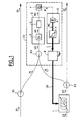
- the resynchronization device shown in the FIG. 1 consists of an adjustable delay device 1, two 1 to 2 couplers K1, K2 and a control unit CU.
- the device receives the input signals E1, E2 and provides resynchronized output signals S1, S2.
- the first input signal El is applied to the input of the first 1 to 2 coupler K1 whose first output provides the first output signal S1 and of which the second output coupled to the CU control unit delivers a first signal measurement optics sl.
- the second input signal E2 is applied to the input of the second coupler K2 by through the delay device 1.
- a first output of coupler K2 provides the second output signal S2 while its second output provides a second signal s2 measurement optics applied to the input of the CU command.
- CU control unit has 2 to 1 coupler K3 whose inputs receive the first and respectively second optical measurement signals s1, s2. Leaving the coupler K3 provides a combination signal s3 which is injected into a non-linear optical device 2.
- the device 2 provides a MO mixing signal to a filter optic F which delivers a filtered signal M to a conversion 5.
- the conversion device 5 provides a control device 8 an electrical control signal C representative of the average signal strength value filtered M.
- the controller 8 provides an electrical control signal CD of the device adjustable delay 1.
- the optical device not linear 2 consists of a fiber optic amplifier 3 coupled to a nonlinear optical medium 4.
- amplifier 3 has the function of injecting into non-linear medium 4 sufficient optical power to bring up intermodulation phenomena research.
- the most suitable nonlinear medium 4 is typically consisting of a semiconductor optical amplifier for which an input optical power of the milliwatt order may be suitable. We could however use other media with properties not linear due to the Kerr effect, such as fibers optical.
- the signals measurement optics s1, s2 have the same polarization.
- the received signals have polarizations we can always plan ahead of the device a known type polarization controller (not represented).
- the conversion device 5 consists of a photodetector 6, for example a photodiode, followed by a low pass electric filter 7.
- the device of figure 1 works in the way next.
- the first optical input signal E1 is received by the first coupler K1 which takes part S1 of the strength of this signal. This part S1 is guided towards a coupler 2 to 1 inputs K3.
- the second signal input E2 passes through delay device 1 to constitute a delayed signal S2 which is injected at the input of the second 1 to 2 coupler K2.
- the coupler K2 takes part s2 of the power of this signal S2 and this part s2 is guided to the other input of the K3 coupler.
- the K3 coupler then provides a combination signal s3 of the signals sl and s2.
- the combination signal s3 is amplified by amplifier 3 so as to provide a signal amplified combination s4 in the nonlinear medium 4.
- the nonlinear medium 4 provides a MO mixing signal containing intermodulation signals whose frequencies optics are of the form p.f1 + q.f2, where p and q are integers relative (and such that the expression is positive).
- Each of the intermodulation signals has a intensity modulation which depends on both modulations intensity of input signals and phase shift of their respective modulation clocks.
- the signal from mixture MO then passes through the filter F which is chosen for transmit an optical frequency band centered on a only intermodulation frequencies f3 and different from f1 and f2.
- the filter F provides the filtered signal M which therefore represents only one of the intermodulation signals.
- the photodetector 6 receives the filtered signal M and provides the low-pass filter 7 with a signal electric detection MC.
- the low-pass filter 7 delivers the electric control signal C which measures the intensity mean optics of the filtered signal M and is therefore representative of the difference between the phases of the clocks of modulation of signals E1 and S2.
- Signal C can then be processed by a type electronic control device conventional 8 designed to control the delay device 1 as a function of signal C so as to impose an offset of phase determined by a Ref.
- the choice of the values of p and q which defines the filter F will be guided by the following considerations.
- the condition necessary is that the frequency f3 is different at the same time of f1 and f2, but it is also desirable that the frequency f3 is in the same frequency range as f1 and f2 of so that you can use an F filter and a photodetector 6 conventional.
- the difference between f1 and f2 is in practice very small compared to f1 or f2
- we will have f3 neighbor of f1 and f2 if we respect the relation p + q 1, with absolute values of p and q of low values.
- Another aspect of implementation concerns the function of filtering carried out by the conversion device 5 so to constitute a device for measuring the average value of the optical intensity of the filtered signal M.
- the constant of conversion device 5 time must be sufficient to do this average. In each particular case it can be evaluated experimentally or by simulations. Thus, for the usual cases of transmission optics, we could for example choose a constant of time in the order of the time interval corresponding to the transmission of a few thousand bits of signals entry.
- the photodetector 6 can already realize a low-pass filtering function, supplemented if necessary by an additional electric low-pass filter 7, as shown in the example in Figure 1.
- the curve of figure 2 represents in percentage the level of the electrical control signal C as a function of ⁇ T in the case where the extinction rate of the signals E1 and E2 is very high.
- Figure 3 shows a similar curve for a TE extinction rate of 13dB. These curves show that the signal C has a maximum value when the offset ⁇ T is zero and a minimum value when ⁇ T is half of the bit T time interval of signals E1 and E2.
- simulations for example allow to establish the law of variation C in function of ⁇ T.
- This law therefore establishes with respect to ⁇ T the transfer function of the set constituted by the devices 2 and 5 in cascade. It is then easy to design a control circuit 8 capable of controlling the delay device 1 so as to impose a value determined (to within T) of the offset ⁇ T.
- control device 8 having for effect of enslaving C to its maximum value. If necessary, we may always impose a determined gap between phases of the two output signals S1 and S2 with a additional delay device (not shown) in output of one of the couplers K1 or K2.
- a realization of the control device 8 can be a circuit well known in the field of regulation which overlaps with low frequency overmodulation to the CD control signal and adjusts this CD control signal so as to make minimum the modulation of the resulting control signal C.
- the variable delay device 1 can be one of the fine adjustment devices commonly used in optical systems.
- a device uses a fiber optic coil, the diameter of which can be modified by a piezoelectric actuator.
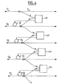
- Figure 4 illustrates how the resynchronization according to the invention can be used for resynchronize between them more than two optical signals, by examples of signals extracted from a length multiplex wave by demultiplexing.
- the assembly shown is organized in several stages receiving by way of example five input signals E1-E5 and providing five resynchronized output signals S1-S5.
- the first two input signals E1, E2 are resynchronized by the first stage which provides the second S2 output signal by means of a first unit of CU1 control arranged in accordance with Figure 1 described previously.
- a second floor with a second unit CU2 resynchronizes the third input signal E3 with respect to the second output signal S2 by providing the third output signal S3.
- a third CU3 control unit resynchronizes S3 and E4 and a fourth control unit CU4 resynchronizes S4 and E5.
- the only adaptation to be envisaged compared to the diagram of the Figure 1 is to provide 1 to 3 couplers at the output delay devices on each stage so as to draw each delayed signal S2-S5 to two units of orders.
- the device that comes to be described is particularly effective in the case where the modulations of the signals E1 and E2 are of type RZ or of soliton type.
- the device can nevertheless be used for NRZ modulations if the input signals present sequences with a large number of frequency transitions bit. Such sequences can for example be sent voluntarily during system initialization.
- the device is not limited to the case where the clock frequencies of the signals input are equal.
- the device can also work if the input signals each have a period whole multiple clock of a common base period.
- the curve representing the variations of the control signal C according to ⁇ T then have several values different amplitudes. This curve can be however, operated by suitable control means 8.
Landscapes
- Physics & Mathematics (AREA)
- Optics & Photonics (AREA)
- Engineering & Computer Science (AREA)
- Computer Networks & Wireless Communication (AREA)
- Signal Processing (AREA)
- Optical Communication System (AREA)
- Optical Modulation, Optical Deflection, Nonlinear Optics, Optical Demodulation, Optical Logic Elements (AREA)
Applications Claiming Priority (2)
| Application Number | Priority Date | Filing Date | Title |
|---|---|---|---|
| FR9801675A FR2774832B1 (fr) | 1998-02-12 | 1998-02-12 | Procede et dispositif de resynchronisation de signaux optiques |
| FR9801675 | 1998-02-12 |
Publications (1)
| Publication Number | Publication Date |
|---|---|
| EP0936773A1 true EP0936773A1 (de) | 1999-08-18 |
Family
ID=9522886
Family Applications (1)
| Application Number | Title | Priority Date | Filing Date |
|---|---|---|---|
| EP99400322A Withdrawn EP0936773A1 (de) | 1998-02-12 | 1999-02-11 | Verfahren und Vorrichtung zur Resynchronisierung optischer Signale |
Country Status (5)
| Country | Link |
|---|---|
| US (1) | US6424443B1 (de) |
| EP (1) | EP0936773A1 (de) |
| JP (1) | JPH11317704A (de) |
| CA (1) | CA2259017A1 (de) |
| FR (1) | FR2774832B1 (de) |
Cited By (3)
| Publication number | Priority date | Publication date | Assignee | Title |
|---|---|---|---|---|
| EP1176751A1 (de) * | 2000-07-27 | 2002-01-30 | Alcatel | Synchronisierungseinrichtung für RZ-WDM Signale und Verfahren zur Synchronisation |
| WO2001050664A3 (de) * | 1999-12-30 | 2002-01-31 | Siemens Ag | Verfahren zur phasensynchronisierung optischer rz-datensignale |
| EP1233567A1 (de) * | 2001-01-25 | 2002-08-21 | Alcatel | Verfahren zur Anpassung von Zeitverzögerungen und Vorrichtung zur Synchronisierung von Kanälen in einem WDM System |
Families Citing this family (2)
| Publication number | Priority date | Publication date | Assignee | Title |
|---|---|---|---|---|
| WO2018141681A1 (en) * | 2017-02-01 | 2018-08-09 | British Telecommunications Public Limited Company | Optical fibre event location |
| CN111051843B (zh) | 2017-07-20 | 2022-03-18 | 英国电讯有限公司 | 光纤 |
Citations (3)
| Publication number | Priority date | Publication date | Assignee | Title |
|---|---|---|---|---|
| EP0619658A2 (de) * | 1993-04-09 | 1994-10-12 | Nec Corporation | Vorrichtung zur optischen Taktgewinnung und Vorrichtung zum Demultiplexen eines Zeitmultiplexsignales |
| US5373381A (en) * | 1989-07-21 | 1994-12-13 | Alfano; Robert R. | Terahertz repetition rate optical computing systems, and communication systems and logic elements using cross-phase modulation based optical processors |
| WO1997044929A1 (en) * | 1996-05-22 | 1997-11-27 | British Telecommunications Public Limited Company | Optical synchronisation arrangement |
Family Cites Families (2)
| Publication number | Priority date | Publication date | Assignee | Title |
|---|---|---|---|---|
| IT1276122B1 (it) * | 1995-11-14 | 1997-10-24 | Pirelli Cavi Spa | Metodo e dispositivo per recuperare in via ottica il sincronismo di un segnale ottico digitale |
| FR2749946B1 (fr) * | 1996-06-14 | 1998-07-31 | Alsthom Cge Alcatel | Dispositif de mise en forme de signaux optiques binaires et son utilisation pour modifier lesdits signaux |
-
1998
- 1998-02-12 FR FR9801675A patent/FR2774832B1/fr not_active Expired - Fee Related
-
1999
- 1999-02-01 CA CA002259017A patent/CA2259017A1/fr not_active Abandoned
- 1999-02-05 US US09/245,334 patent/US6424443B1/en not_active Expired - Fee Related
- 1999-02-10 JP JP11033452A patent/JPH11317704A/ja active Pending
- 1999-02-11 EP EP99400322A patent/EP0936773A1/de not_active Withdrawn
Patent Citations (3)
| Publication number | Priority date | Publication date | Assignee | Title |
|---|---|---|---|---|
| US5373381A (en) * | 1989-07-21 | 1994-12-13 | Alfano; Robert R. | Terahertz repetition rate optical computing systems, and communication systems and logic elements using cross-phase modulation based optical processors |
| EP0619658A2 (de) * | 1993-04-09 | 1994-10-12 | Nec Corporation | Vorrichtung zur optischen Taktgewinnung und Vorrichtung zum Demultiplexen eines Zeitmultiplexsignales |
| WO1997044929A1 (en) * | 1996-05-22 | 1997-11-27 | British Telecommunications Public Limited Company | Optical synchronisation arrangement |
Cited By (6)
| Publication number | Priority date | Publication date | Assignee | Title |
|---|---|---|---|---|
| WO2001050664A3 (de) * | 1999-12-30 | 2002-01-31 | Siemens Ag | Verfahren zur phasensynchronisierung optischer rz-datensignale |
| US7312909B2 (en) | 1999-12-30 | 2007-12-25 | Siemens Aktiengesellschaft | Method for synchronizing the phase of optical return-to-zero (RZ) data signals |
| EP1176751A1 (de) * | 2000-07-27 | 2002-01-30 | Alcatel | Synchronisierungseinrichtung für RZ-WDM Signale und Verfahren zur Synchronisation |
| WO2002011354A1 (en) * | 2000-07-27 | 2002-02-07 | Alcatel | Synchronizer for rz-wdm signals and method for synchronization |
| EP1233567A1 (de) * | 2001-01-25 | 2002-08-21 | Alcatel | Verfahren zur Anpassung von Zeitverzögerungen und Vorrichtung zur Synchronisierung von Kanälen in einem WDM System |
| US7187869B2 (en) | 2001-01-25 | 2007-03-06 | Alcatel | Method for adjusting time delays and device for synchronization of channels in a WDM system |
Also Published As
| Publication number | Publication date |
|---|---|
| FR2774832B1 (fr) | 2000-08-04 |
| FR2774832A1 (fr) | 1999-08-13 |
| US6424443B1 (en) | 2002-07-23 |
| CA2259017A1 (fr) | 1999-08-12 |
| JPH11317704A (ja) | 1999-11-16 |
Similar Documents
| Publication | Publication Date | Title |
|---|---|---|
| EP1111820A1 (de) | Einrichtung zum Anbringen von einer Verzögerung | |
| EP0975107B1 (de) | Sendevorrichtung für optische Daten | |
| EP0718992B1 (de) | Vorrichtung zum Inline-Regenerieren eines Solitonsignals durch synchrone Modulation der Solitone mit einem nicht-linearen optischen Spiegel | |
| EP0813097B1 (de) | Vorrichtung zur Regeneration digitaler optischer Signale und ihre Verwendung zur Veränderung derartiger Signale | |
| FR2761490A1 (fr) | Circuit de detection de positions d'impulsions optiques, appareil de production d'impulsions optiques et procedes pour leur utilisation | |
| EP0862286A1 (de) | Optische Regenerierung für faseroptische Übertragungssysteme mit nicht-Soliton Signalen | |
| EP0763912B1 (de) | Rein optischer Frequenzverdoppler und dieser verwendender Solitonregenerator | |
| FR2762732A1 (fr) | Procede et dispositif de decompression d'impulsions constituant un signal optique binaire | |
| CA2093991C (fr) | Source d'impulsion optique et systeme de transmission optique a solitons comportant cette source | |
| FR2799070A1 (fr) | Regenerateur de signaux optiques multiplexes en longueur d'onde | |
| EP0936773A1 (de) | Verfahren und Vorrichtung zur Resynchronisierung optischer Signale | |
| EP0852436B1 (de) | Solitonregenerator mit sehr hoher Datenrate | |
| EP0871304B1 (de) | Verfahren und Vorrichtung zur Formung eines optischen binären Signales | |
| EP0975106B1 (de) | Anordnung zum Inline-Regenerieren eines optischen Solitonsignals durch synchrone Modulation dieser Solitonen und Übertragungssystem mit einer derartigen Vorrichtung | |
| EP1497939A1 (de) | Optische vorrichtung und verfahren zur umwandlung eines wdm-signals in ein otdm-signal und umgekehrt | |
| EP0746070B1 (de) | Verfahren und Vorrichtung zur Kombination optischer Signale | |
| FR2797331A1 (fr) | Differenciateur optique | |
| EP1158352A2 (de) | Optischer NRZ-RZ-Wandler | |
| WO2002019574A1 (fr) | Regenerateur tout-optique pour signaux multiplexes en longueur d'onde | |
| EP3168679A1 (de) | Vorrichtung zur modulierung der intensität eines optischen signals auf vier verschiedenen ebenen | |
| CA2376153A1 (fr) | Regenerateur avec restitution d'une onde porteuse d'un signal optique | |
| EP0652653A1 (de) | Faseroptisches Übertragungsverfahren, Verbindung dazu und Pumpgerät für Vierzwellenmischung, insbesondere für diese Verbindung | |
| FR2803399A1 (fr) | Dispositif de generation de porteuses pour systeme de transmission optique a multiplexage en longueur d'onde a signaux rz | |
| FR2715255A1 (fr) | Procédé de transmission optique par solitons, à faible densité spectrale aux fréquences basses émetteur et récepteur correspondants. | |
| FR2879053A1 (fr) | Dispositif regenerateur 2r/3r tout-optique a base d'un unique modulateur a electroabsorption |
Legal Events
| Date | Code | Title | Description |
|---|---|---|---|
| PUAI | Public reference made under article 153(3) epc to a published international application that has entered the european phase |
Free format text: ORIGINAL CODE: 0009012 |
|
| AK | Designated contracting states |
Kind code of ref document: A1 Designated state(s): DE FI GB IT SE |
|
| AX | Request for extension of the european patent |
Free format text: AL;LT;LV;MK;RO;SI |
|
| 17P | Request for examination filed |
Effective date: 20000218 |
|
| AKX | Designation fees paid |
Free format text: DE FI GB IT SE |
|
| 17Q | First examination report despatched |
Effective date: 20040421 |
|
| STAA | Information on the status of an ep patent application or granted ep patent |
Free format text: STATUS: THE APPLICATION IS DEEMED TO BE WITHDRAWN |
|
| 18D | Application deemed to be withdrawn |
Effective date: 20041001 |