EP1158352A2 - Optischer NRZ-RZ-Wandler - Google Patents
Optischer NRZ-RZ-Wandler Download PDFInfo
- Publication number
- EP1158352A2 EP1158352A2 EP01401282A EP01401282A EP1158352A2 EP 1158352 A2 EP1158352 A2 EP 1158352A2 EP 01401282 A EP01401282 A EP 01401282A EP 01401282 A EP01401282 A EP 01401282A EP 1158352 A2 EP1158352 A2 EP 1158352A2
- Authority
- EP
- European Patent Office
- Prior art keywords
- signal
- output
- arms
- nrz
- optical
- Prior art date
- Legal status (The legal status is an assumption and is not a legal conclusion. Google has not performed a legal analysis and makes no representation as to the accuracy of the status listed.)
- Withdrawn
Links
- 230000003287 optical effect Effects 0.000 title claims abstract description 59
- 238000006243 chemical reaction Methods 0.000 claims description 13
- 230000008878 coupling Effects 0.000 claims description 12
- 238000010168 coupling process Methods 0.000 claims description 12
- 238000005859 coupling reaction Methods 0.000 claims description 12
- 238000000034 method Methods 0.000 claims description 5
- 230000001066 destructive effect Effects 0.000 claims description 3
- 238000011144 upstream manufacturing Methods 0.000 claims 1
- 230000005540 biological transmission Effects 0.000 description 10
- 235000021183 entrée Nutrition 0.000 description 7
- 239000004065 semiconductor Substances 0.000 description 6
- 230000008901 benefit Effects 0.000 description 4
- 230000008859 change Effects 0.000 description 3
- 230000003111 delayed effect Effects 0.000 description 3
- 230000010287 polarization Effects 0.000 description 3
- 239000000835 fiber Substances 0.000 description 2
- 230000006872 improvement Effects 0.000 description 2
- 230000010363 phase shift Effects 0.000 description 2
- 230000009466 transformation Effects 0.000 description 2
- 101100326341 Drosophila melanogaster brun gene Proteins 0.000 description 1
- 240000000018 Gnetum gnemon Species 0.000 description 1
- 240000008042 Zea mays Species 0.000 description 1
- 230000003321 amplification Effects 0.000 description 1
- 238000010586 diagram Methods 0.000 description 1
- 239000006185 dispersion Substances 0.000 description 1
- 238000005516 engineering process Methods 0.000 description 1
- 238000004519 manufacturing process Methods 0.000 description 1
- 238000003199 nucleic acid amplification method Methods 0.000 description 1
- 239000013307 optical fiber Substances 0.000 description 1
- 230000005693 optoelectronics Effects 0.000 description 1
- 230000008569 process Effects 0.000 description 1
- 230000001902 propagating effect Effects 0.000 description 1
- 238000011084 recovery Methods 0.000 description 1
- 238000000926 separation method Methods 0.000 description 1
- 239000000758 substrate Substances 0.000 description 1
Images


Classifications
-
- G—PHYSICS
- G02—OPTICS
- G02F—OPTICAL DEVICES OR ARRANGEMENTS FOR THE CONTROL OF LIGHT BY MODIFICATION OF THE OPTICAL PROPERTIES OF THE MEDIA OF THE ELEMENTS INVOLVED THEREIN; NON-LINEAR OPTICS; FREQUENCY-CHANGING OF LIGHT; OPTICAL LOGIC ELEMENTS; OPTICAL ANALOGUE/DIGITAL CONVERTERS
- G02F1/00—Devices or arrangements for the control of the intensity, colour, phase, polarisation or direction of light arriving from an independent light source, e.g. switching, gating or modulating; Non-linear optics
- G02F1/01—Devices or arrangements for the control of the intensity, colour, phase, polarisation or direction of light arriving from an independent light source, e.g. switching, gating or modulating; Non-linear optics for the control of the intensity, phase, polarisation or colour
- G02F1/21—Devices or arrangements for the control of the intensity, colour, phase, polarisation or direction of light arriving from an independent light source, e.g. switching, gating or modulating; Non-linear optics for the control of the intensity, phase, polarisation or colour by interference
- G02F1/225—Devices or arrangements for the control of the intensity, colour, phase, polarisation or direction of light arriving from an independent light source, e.g. switching, gating or modulating; Non-linear optics for the control of the intensity, phase, polarisation or colour by interference in an optical waveguide structure
-
- G—PHYSICS
- G02—OPTICS
- G02F—OPTICAL DEVICES OR ARRANGEMENTS FOR THE CONTROL OF LIGHT BY MODIFICATION OF THE OPTICAL PROPERTIES OF THE MEDIA OF THE ELEMENTS INVOLVED THEREIN; NON-LINEAR OPTICS; FREQUENCY-CHANGING OF LIGHT; OPTICAL LOGIC ELEMENTS; OPTICAL ANALOGUE/DIGITAL CONVERTERS
- G02F2/00—Demodulating light; Transferring the modulation of modulated light; Frequency-changing of light
- G02F2/004—Transferring the modulation of modulated light, i.e. transferring the information from one optical carrier of a first wavelength to a second optical carrier of a second wavelength, e.g. all-optical wavelength converter
-
- G—PHYSICS
- G02—OPTICS
- G02F—OPTICAL DEVICES OR ARRANGEMENTS FOR THE CONTROL OF LIGHT BY MODIFICATION OF THE OPTICAL PROPERTIES OF THE MEDIA OF THE ELEMENTS INVOLVED THEREIN; NON-LINEAR OPTICS; FREQUENCY-CHANGING OF LIGHT; OPTICAL LOGIC ELEMENTS; OPTICAL ANALOGUE/DIGITAL CONVERTERS
- G02F1/00—Devices or arrangements for the control of the intensity, colour, phase, polarisation or direction of light arriving from an independent light source, e.g. switching, gating or modulating; Non-linear optics
- G02F1/01—Devices or arrangements for the control of the intensity, colour, phase, polarisation or direction of light arriving from an independent light source, e.g. switching, gating or modulating; Non-linear optics for the control of the intensity, phase, polarisation or colour
- G02F1/21—Devices or arrangements for the control of the intensity, colour, phase, polarisation or direction of light arriving from an independent light source, e.g. switching, gating or modulating; Non-linear optics for the control of the intensity, phase, polarisation or colour by interference
- G02F1/212—Mach-Zehnder type
-
- G—PHYSICS
- G02—OPTICS
- G02F—OPTICAL DEVICES OR ARRANGEMENTS FOR THE CONTROL OF LIGHT BY MODIFICATION OF THE OPTICAL PROPERTIES OF THE MEDIA OF THE ELEMENTS INVOLVED THEREIN; NON-LINEAR OPTICS; FREQUENCY-CHANGING OF LIGHT; OPTICAL LOGIC ELEMENTS; OPTICAL ANALOGUE/DIGITAL CONVERTERS
- G02F1/00—Devices or arrangements for the control of the intensity, colour, phase, polarisation or direction of light arriving from an independent light source, e.g. switching, gating or modulating; Non-linear optics
- G02F1/35—Non-linear optics
- G02F1/3515—All-optical modulation, gating, switching, e.g. control of a light beam by another light beam
- G02F1/3517—All-optical modulation, gating, switching, e.g. control of a light beam by another light beam using an interferometer
-
- G—PHYSICS
- G02—OPTICS
- G02F—OPTICAL DEVICES OR ARRANGEMENTS FOR THE CONTROL OF LIGHT BY MODIFICATION OF THE OPTICAL PROPERTIES OF THE MEDIA OF THE ELEMENTS INVOLVED THEREIN; NON-LINEAR OPTICS; FREQUENCY-CHANGING OF LIGHT; OPTICAL LOGIC ELEMENTS; OPTICAL ANALOGUE/DIGITAL CONVERTERS
- G02F2201/00—Constructional arrangements not provided for in groups G02F1/00 - G02F7/00
- G02F2201/20—Constructional arrangements not provided for in groups G02F1/00 - G02F7/00 delay line
-
- G—PHYSICS
- G02—OPTICS
- G02F—OPTICAL DEVICES OR ARRANGEMENTS FOR THE CONTROL OF LIGHT BY MODIFICATION OF THE OPTICAL PROPERTIES OF THE MEDIA OF THE ELEMENTS INVOLVED THEREIN; NON-LINEAR OPTICS; FREQUENCY-CHANGING OF LIGHT; OPTICAL LOGIC ELEMENTS; OPTICAL ANALOGUE/DIGITAL CONVERTERS
- G02F2203/00—Function characteristic
- G02F2203/26—Pulse shaping; Apparatus or methods therefor
Definitions
- the invention lies in the field of "all optical" converters to convert a signal entering NRZ format as an RZ output signal. She also relates to a conversion process.
- the bandwidth bandwidth required to transmit at the same speed data in RZ format and the same data in format NRZ is more than double in the case of the RZ format.
- the RZ format is also interesting in some applications, for example the multiplexing, demultiplexing by passive division of time, the soliton generation, and the removal of the stimulated dispersion of BRILLOUIN.
- the interferometer receives a train on the one hand regular pulses and on the other hand a signal at format without return to 0 representative of a signal data.
- the power levels of the two signals are choose so that if only one of the signals is present, that is to say is at the high level, a destructive interference occurs so the signal level at the output of the interferometer is low, which corresponds to normal operation a SAGNAC interferometer, taking into account the delay of phase between the direct signal and the signal opposite direction resulting from the birefringent nature of the fiber.
- a SAGNAC interferometer taking into account the delay of phase between the direct signal and the signal opposite direction resulting from the birefringent nature of the fiber.
- an additional phase of ⁇ is caused by modulation of the high power signal propagating in opposite directions and therefore by a constructive interference at the exit of the interferometer.
- the device thus behaves like a door "and".
- a signal RZ resulting from the conversion of the NRZ signal either on a carrier at wavelength carrying the train of pulses, i.e. at the wavelength carrying the NRZ signal.
- a second embodiment of a NRZ - RZ converter is described in an article by S. BIGO, E. DESURVIRE, S. GAUCHARD and E. BRUN entitled “Speed improvement by optical conversion NRZ - RZ and passive time division multiplexing for soliton transmission systems ", published in "Electronics Letters" newspaper of June 9, 1994 (vol. 30, No. 12, pages 984, 985).
- S. BIGO E. DESURVIRE
- S. GAUCHARD S. GAUCHARD
- E. BRUN entitled “Speed improvement by optical conversion NRZ - RZ and passive time division multiplexing for soliton transmission systems ", published in "Electronics Letters" newspaper of June 9, 1994 (vol. 30, No. 12, pages 984, 985).
- it is used a non-linear optical loop mirror.
- two signals are introduced in the SAGNAC interferometer loop.
- control signal it is introduced on the one hand, a control signal to a wavelength ⁇ c and, on the other hand, an NRZ signal at the wavelength ⁇ s.
- a polarization controller the interferometer is adjusted so as to minimize the output signal when the control signal is low so as to obtain a SAGNAC interferometer.
- the control signal is introduced into the loop forming the interferometer through a 80/20 coupler located near the point of sharing between the direct wave and the reverse wave.
- the pulse width of the RZ signal is slightly less than the pulse width of control at the wavelength ⁇ c.
- the difference in level between low level and high level is more than 20 dB representing a 10-fold improvement over in the previous example with active loop.
- fiber loop mirrors are very sensitive to polarization of light and temperature fluctuations.
- a third embodiment example is mentioned in an article by David NORTE and Allan E. WILLNER entitled “Experimental demonstration of a all-optical conversion between data in formats RZ and NRZ incorporating non-inverting changes in wavelength and leading to transparency of the format ", published in” IEEE photonics technology letters " (vol. n ° 8, n ° 5 - May 1996, pages 712-714).
- the device mentioned in this article concerns an RZ - NRZ converter whose diagram is shown in Figure 1 of this article.
- the description of the device and its operation are made little clear by the fact that an optical amplifier SOA1 mentioned in the text is not shown on the figure. We understand, however, that first of all recover the clock signal from the RZ signal. It is also explained that a device not described allows to pass from a NRZ format to a format RZ so that one can have one or the other format.
- Each of the devices described or mentioned in these articles are subsystems that include several optoelectronic devices or electronic and require assembly work. As mentioned above, those based on interferometers of SAGNAC are sensitive to fluctuations in temperature or polarization of light. All devices described in these articles require a clock signal or clock recovery.
- the idea behind the invention is to use an interferometric structure for example of Mach-Zehnder with two arms, a first and a second. At least one of the first and second arms has a element whose optical index may vary depending of the optical power present in this element, by example a semiconductor optical amplifier (SOA).
- SOA semiconductor optical amplifier
- the two signals from the input signal (Se) present in each of the arms of the interferometer destroy themselves at the exit of the interferometer.
- the interferometer therefore behaves like a door optics whose opening is controlled by a signal from control (Sc).
- this phenomenon to convert a signal to NRZ format as signal in RZ format, without using optical clock signal.
- the signal present in exit from the interferometer giving it a time delay substantially equal to half the time bit of NRZ signal.
- the delayed output signal is used well control signal to close or open the optical door described above.
- the time delay allows to temporarily remove optical power in the interferometer output signal. We so gets as will be seen in more detail more away an output signal corresponding to the signal input but in RZ format.
- the active media including the refractive index is sensitive to the power which crosses, are made up of active layers semiconductor optical amplifier.
- the bit time is very short, on the order of a few tens of picoseconds and the delay in the signal reintroduced into one of the arms may be produced for example by means of an integrated optical guide on a substrate of the interferometer or of a component, for example an optical amplifier, also having function to adjust the level of the front output signal its reintroduction in one of the arms of the structure interferometric.
- the signal at the output of the structure interferometric can be introduced on the end of the arm of the structure also receiving the signal NRZ to convert so that the two signals get propagate in this arm in the same direction. In this case it will be better to convert to wavelength the signal at the output of the structure to avoid interference between these two signals occurring in said arm.
- the signal at the output of the structure interferometric can also be introduced on a end of the arm of the structure which is opposite to the one receiving the NRZ signal. In this case, it will possible or not to convert into wavelength, the signal at the output of the interferometric structure before its introduction into said arm of the structure.
- the paths optics of the two arms of the structure are equal, thus causing constructive interference between signals present in each of the arms.
- means placed between the exit from the structure and one of the arms adjusts the optical power level of the signal present at the output so as to modify the optical path of one of the arms relative to each other to get interference destructive.
- Figure 1 shows schematically a first example of an NRZ converter - RZ according to the invention.
- This converter uses a structure interferometric 10, in itself known, which will be described below.
- This structure is presented in a way balanced and has two control inputs 1, 4 with their balanced 5, 8, two signal inputs 2-3 with their symmetrical output 6-7. Entrances 2 and 3 are coupled to each of the arms 9, 11 of the structure.
- Each of the arms has two ends, one first 26, 28 respectively and a second 27, 29 respectively.
- inputs 2, 3 are first coupled together, then separated and coupled as shown in Figures 1, 3, and 4 on each of the arms 9, 11.
- These coupling means constituting the coupling at each of the arms 9, 11 have been identified by the reference 23. They constitute a 2 to 2 coupler. symmetrically on the output side, the coupling means consist of another 2 to 2 coupler marked 23 '.
- Control inputs 1, 4 are each coupled to one of the arms 9, 11 so that a signal introduced on these arms through these inputs spreads in the arm from the first to the second end of this arms.
- control inputs 5, 8 are each coupled to one of the arms 9, 11 respectively.
- the signals input by the control input 5 by example spread from the second end 27 of the arm 9 at the first end 26 of this arm.
- control inputs 4 and 8 Only the means of coupling of these inputs at each of the ends 28, 29 arm 11 respectively have been referenced 24 and 24 ' respectively.
- Each of the arms 9, 11 is equipped with a middle optics 13, 15 of variable index with power optic passing through it, in the form of a layer active of a semiconductor amplifier.
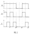
- level of control input 4 or 8 0 0 1 1 signal input level 2 0 1 0 1 output level 7 0 1 0 0 level of control input 1 or 5 0 0 1 1 signal input level 3 0 1 0 1 output level 6 0 1 0 0 0
- control signal - i.e. level of control input at 0 - the signal present at the input 3 is reproduced at output 6.
- the signal control is at the high level, i.e. at the value 1, an input signal at level 0 or level 1 is transformed into an output signal at level 0.
- Part A represents the variations over time of the level of a NRZ signal whose bit time duration is T. It is assumed that such a signal is entered on the input 2.
- the signal at output 7 is fed back to the control input 8 with a delay time equal to half a period of time bit T.
- T time bit
- the bit rate is equal to 10 Gigabits
- the time bit is 10 -10 seconds or 100 picoseconds.
- a delay of T / 2 is 50 picoseconds.
- Such a delay can be obtained with only one cm of optical fiber or with a 5 mm long InP guide.
- the signal present at output 7 is re-amplified to be upgraded suitable for obtaining a level close to the saturation of the active optical medium of the amplifier present on the arm 11.
- an optical amplifier 14 which receives the optical signal at signal output 7 is used both as an amplifier 14 and as a medium T / 2 delay 16.
- the return signal, delayed by T / 2 is introduced on control input 8 so that this signal propagates in this arm in the opposite direction of the NRZ signal introduced on input 2.
- This reintroduced signal is therefore propagates from the second 29 to the first 28 end of arm 11.
- the return signal does not interfere with the NRZ signal to transform. It only change the power level at the right times present in the active medium 15 of the amplifier arm optic 11.
- the converted RZ signal is on a carrier at the same wavelength as the signal Entry NRZ.
- FIG. 3 represents an embodiment of the invention having the advantage of being able to change the wavelength of the level control signal power passing through the optical amplifier 15.
- the device shown in Figure 3 includes a device 10 as shown in FIG. 1 comprising the elements designated by the references 1-9, 11-13 and 15, 23-24 '.
- the output 7 leads to a filter 17.
- the signal at the output of filter 17 feeds a loop of return 30 comprising a converter 19 of length wave, which feeds preferably through a band pass filter 20 control input 4.
- the converter 19 includes means to adjust the output level of this converter.
- the filter 17 at output 7 of the device 10 is a bandpass filter centered on the wavelength carrier of the NRZ signal.
- the filter 20 at the output of the converter 19 is a bandpass filter centered on the wavelength of the control signal generated or received by the converter 19.
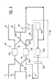
- FIG. 4 shows an example of realization of the wavelength converter 19.
- Wave generation at wavelength control is carried out for example by means of a laser diode 21.
- the output signal from diode 21 in the form of an unmodulated continuous wave is coupled to the signal at the output of filter 17 and the two signals are introduced into an optical amplifier at semiconductor 22 having an active medium sensitive to optical power passing through it.
- the input power of each of the incoming signals in amplifier 22 is such that we reach the saturation value when the value of the modulated signal from filter 17 is high, then the wave continuous from diode 21 is modulated as this signal.
- set the transit time in the converter 19 so that it is substantially equal to T / 2.
- Figures 3 and 4 show the device according to the invention with the outlet of the converter 19 coupled to the first end 28 of the arm 11. Naturally, it is also possible to couple to the second end 29, so that the NRZ signal and the control signal propagate in reverse.
- control signal is also the output signal, i.e. the RZ signal resulting from the conversion of the NRZ signal.
Landscapes
- Physics & Mathematics (AREA)
- Nonlinear Science (AREA)
- General Physics & Mathematics (AREA)
- Optics & Photonics (AREA)
- Optical Communication System (AREA)
- Optical Modulation, Optical Deflection, Nonlinear Optics, Optical Demodulation, Optical Logic Elements (AREA)
- Signal Processing For Digital Recording And Reproducing (AREA)
Applications Claiming Priority (2)
| Application Number | Priority Date | Filing Date | Title |
|---|---|---|---|
| FR0006548A FR2809497B1 (fr) | 2000-05-23 | 2000-05-23 | Convertisseur optique de format nrz-rz |
| FR0006548 | 2000-05-23 |
Publications (2)
| Publication Number | Publication Date |
|---|---|
| EP1158352A2 true EP1158352A2 (de) | 2001-11-28 |
| EP1158352A3 EP1158352A3 (de) | 2003-12-17 |
Family
ID=8850498
Family Applications (1)
| Application Number | Title | Priority Date | Filing Date |
|---|---|---|---|
| EP01401282A Withdrawn EP1158352A3 (de) | 2000-05-23 | 2001-05-17 | Optischer NRZ-RZ-Wandler |
Country Status (4)
| Country | Link |
|---|---|
| US (1) | US6625338B2 (de) |
| EP (1) | EP1158352A3 (de) |
| JP (1) | JP2002031825A (de) |
| FR (1) | FR2809497B1 (de) |
Families Citing this family (5)
| Publication number | Priority date | Publication date | Assignee | Title |
|---|---|---|---|---|
| GB0201677D0 (en) * | 2002-01-25 | 2002-03-13 | Glaxo Group Ltd | Medicament dispenser |
| CN100442136C (zh) * | 2006-12-28 | 2008-12-10 | 华中科技大学 | 一种非归零码到归零码全光码型转换装置 |
| CN100442137C (zh) * | 2006-12-28 | 2008-12-10 | 华中科技大学 | 基于非线性光波导环形镜的全光码型转换装置 |
| WO2013013695A1 (en) * | 2011-07-22 | 2013-01-31 | Telefonaktiebolaget L M Ericsson (Publ) | An optical switch and a method of switching an optical signal |
| CN102594457B (zh) * | 2012-03-05 | 2014-05-28 | 西南交通大学 | 一种针对复用信号的多功能可调谐全光码型转换器 |
Family Cites Families (4)
| Publication number | Priority date | Publication date | Assignee | Title |
|---|---|---|---|---|
| FR2759790B1 (fr) * | 1997-02-14 | 1999-03-26 | Alsthom Cge Alcatel | Convertisseur de longueur d'onde de signaux optiques binaires |
| FR2778250B1 (fr) * | 1998-04-30 | 2000-06-02 | Alsthom Cge Alcatel | Dispositif de mise en forme de signaux optiques binaires |
| JP3439345B2 (ja) * | 1998-06-29 | 2003-08-25 | 日本電気株式会社 | 波長変換器及び波長変換方法 |
| GB2354598A (en) * | 1999-09-27 | 2001-03-28 | Cit Alcatel | An optical modulator |
-
2000
- 2000-05-23 FR FR0006548A patent/FR2809497B1/fr not_active Expired - Fee Related
-
2001
- 2001-05-10 US US09/852,175 patent/US6625338B2/en not_active Expired - Fee Related
- 2001-05-17 EP EP01401282A patent/EP1158352A3/de not_active Withdrawn
- 2001-05-18 JP JP2001148678A patent/JP2002031825A/ja not_active Withdrawn
Non-Patent Citations (3)
| Title |
|---|
| BIGO S ET AL: "BIT-RATE ENHANCEMENT THROUGH OPTICAL NRZ-TO-RZ CONVERSION AND PASSIVE TIME-DIVISION MULTIPLEXING FOR SOLITON TRANSMISSION SYSTEMS" ELECTRONICS LETTERS,GB,IEE STEVENAGE, vol. 30, no. 12, 9 juin 1994 (1994-06-09), pages 984-985, XP000459796 ISSN: 0013-5194 * |
| KOLLECK C ET AL: "ALL-OPTICAL WAVELENGTH CONVERSION OF NRZ AND RZ SIGNALS USING A NONLINEAR OPTICAL LOOP MIRROR" JOURNAL OF LIGHTWAVE TECHNOLOGY,US,IEEE. NEW YORK, vol. 15, no. 10, 1 octobre 1997 (1997-10-01), pages 1906-1913, XP000703609 ISSN: 0733-8724 * |
| TAKAYAMA K ET AL: "An all-optical 10-GHz LD-based clock regenerator using a Mach-Zehnder-interferometer-type NRZ-to-RZ converter" IOOC-ECOC '91. 17TH EUROPEAN CONFERENCE ON OPTICAL COMMUNICATION ECOC '91. 8TH INTERNATIONAL CONFERENCE ON INTEGRATED OPTICS AND OPTICAL FIBRE COMMUNICATION IOOC '91, PARIS, FRANCE, 9-12 SEPT. 1991, pages 77-80 vol.1, XP000980333 1991, Valbonne, France, SEE, France * |
Also Published As
| Publication number | Publication date |
|---|---|
| EP1158352A3 (de) | 2003-12-17 |
| US20020018612A1 (en) | 2002-02-14 |
| US6625338B2 (en) | 2003-09-23 |
| FR2809497A1 (fr) | 2001-11-30 |
| JP2002031825A (ja) | 2002-01-31 |
| FR2809497B1 (fr) | 2002-10-04 |
Similar Documents
| Publication | Publication Date | Title |
|---|---|---|
| EP0017571B1 (de) | Lichtintensitätsmodulator in integrierter Optik und integrierte optische Schaltung mit einem solchen Modulator | |
| EP0780723B1 (de) | Steuerbarer Amplitude- und Phasenmodulator und Solitonregenerator mit einem solchen Modulator | |
| FR2715524A1 (fr) | Système de communication de type soliton optique ainsi qu'émetteur et récepteur optiques pour ce système. | |
| EP0718992B1 (de) | Vorrichtung zum Inline-Regenerieren eines Solitonsignals durch synchrone Modulation der Solitone mit einem nicht-linearen optischen Spiegel | |
| CA2196333C (fr) | Modulateur kerr independant de la polarisation, et dispositif de recuperation toute optique d'horloge comprenant un tel modulateur | |
| EP1111820A1 (de) | Einrichtung zum Anbringen von einer Verzögerung | |
| EP1162769B1 (de) | Vorrichtung zum Regenerieren optischer Signale | |
| EP0763912B1 (de) | Rein optischer Frequenzverdoppler und dieser verwendender Solitonregenerator | |
| EP0788017B1 (de) | Polarisationsunabhängiger nichtlinearer optischer Ringspiegel (NOLM) | |
| EP0716486B1 (de) | Wellenlängenkonverter | |
| EP1087553A1 (de) | Optischer Regenerator für WDM Signalen | |
| EP1158352A2 (de) | Optischer NRZ-RZ-Wandler | |
| FR2522225A1 (fr) | Dispositif de telecommunication a fibre optique unimodale | |
| FR2736480A1 (fr) | Disposif de coloration de signaux optiques | |
| EP0094866B1 (de) | Gerät für busartige wechselseitige Verbindung mit monomoden Lichtwellenleitern | |
| EP0802640A1 (de) | Verfahren und Vorrichtung zur Verstärkung von Kanälen aus Wellenlängenmultiplex aufbereitet | |
| EP0975106B1 (de) | Anordnung zum Inline-Regenerieren eines optischen Solitonsignals durch synchrone Modulation dieser Solitonen und Übertragungssystem mit einer derartigen Vorrichtung | |
| FR2797331A1 (fr) | Differenciateur optique | |
| CA2275739A1 (fr) | Dispositif de compensation de la dispersion de polarisation des canaux dans un signal a multiplexage en longueur d'onde | |
| EP0746070B1 (de) | Verfahren und Vorrichtung zur Kombination optischer Signale | |
| EP2171535B1 (de) | Faseroptische tür mit hoher zeitauflösung | |
| EP0936773A1 (de) | Verfahren und Vorrichtung zur Resynchronisierung optischer Signale | |
| FR2813466A1 (fr) | Regenerateur tout-optique pour signaux multiplexes en longueur d'onde | |
| WO2024002925A1 (fr) | Procédé et dispositif de filtrage optique à réponse impulsionnelle finie et équipements optiques correspondants | |
| WO2009062888A1 (fr) | Dispositif de réplication optique à taux élevé de répétition |
Legal Events
| Date | Code | Title | Description |
|---|---|---|---|
| PUAI | Public reference made under article 153(3) epc to a published international application that has entered the european phase |
Free format text: ORIGINAL CODE: 0009012 |
|
| AK | Designated contracting states |
Kind code of ref document: A2 Designated state(s): AT BE CH CY DE DK ES FI FR GB GR IE IT LI LU MC NL PT SE TR |
|
| AX | Request for extension of the european patent |
Free format text: AL;LT;LV;MK;RO;SI |
|
| PUAL | Search report despatched |
Free format text: ORIGINAL CODE: 0009013 |
|
| AK | Designated contracting states |
Kind code of ref document: A3 Designated state(s): AT BE CH CY DE DK ES FI FR GB GR IE IT LI LU MC NL PT SE TR |
|
| AX | Request for extension of the european patent |
Extension state: AL LT LV MK RO SI |
|
| RIC1 | Information provided on ipc code assigned before grant |
Ipc: 7H 04B 10/00 B Ipc: 7G 02F 1/225 A |
|
| RAP1 | Party data changed (applicant data changed or rights of an application transferred) |
Owner name: AVANEX CORPORATION |
|
| 17P | Request for examination filed |
Effective date: 20040601 |
|
| AKX | Designation fees paid |
Designated state(s): AT BE CH CY DE DK ES FI FR GB GR IE IT LI LU MC NL PT SE TR |
|
| STAA | Information on the status of an ep patent application or granted ep patent |
Free format text: STATUS: THE APPLICATION HAS BEEN WITHDRAWN |
|
| 18W | Application withdrawn |
Effective date: 20050525 |