EP0938073A2 - Circuit et dispositif de commande d'un panneau d'affichage à plasma - Google Patents
Circuit et dispositif de commande d'un panneau d'affichage à plasma Download PDFInfo
- Publication number
- EP0938073A2 EP0938073A2 EP99301271A EP99301271A EP0938073A2 EP 0938073 A2 EP0938073 A2 EP 0938073A2 EP 99301271 A EP99301271 A EP 99301271A EP 99301271 A EP99301271 A EP 99301271A EP 0938073 A2 EP0938073 A2 EP 0938073A2
- Authority
- EP
- European Patent Office
- Prior art keywords
- scan
- pulse
- driving
- pulses
- driving block
- Prior art date
- Legal status (The legal status is an assumption and is not a legal conclusion. Google has not performed a legal analysis and makes no representation as to the accuracy of the status listed.)
- Withdrawn
Links
- 238000000034 method Methods 0.000 title claims abstract description 67
- 230000009189 diving Effects 0.000 claims 1
- 208000028659 discharge Diseases 0.000 description 88
- 239000000758 substrate Substances 0.000 description 14
- 238000010586 diagram Methods 0.000 description 11
- 235000019557 luminance Nutrition 0.000 description 9
- 238000005192 partition Methods 0.000 description 3
- 230000000977 initiatory effect Effects 0.000 description 2
- 238000012986 modification Methods 0.000 description 2
- 230000004048 modification Effects 0.000 description 2
- 230000000694 effects Effects 0.000 description 1
- 230000001939 inductive effect Effects 0.000 description 1
- 239000011261 inert gas Substances 0.000 description 1
- 239000004973 liquid crystal related substance Substances 0.000 description 1
- 239000000463 material Substances 0.000 description 1
- 230000002459 sustained effect Effects 0.000 description 1
- 230000001360 synchronised effect Effects 0.000 description 1
Images






Classifications
-
- G—PHYSICS
- G09—EDUCATION; CRYPTOGRAPHY; DISPLAY; ADVERTISING; SEALS
- G09G—ARRANGEMENTS OR CIRCUITS FOR CONTROL OF INDICATING DEVICES USING STATIC MEANS TO PRESENT VARIABLE INFORMATION
- G09G3/00—Control arrangements or circuits, of interest only in connection with visual indicators other than cathode-ray tubes
- G09G3/20—Control arrangements or circuits, of interest only in connection with visual indicators other than cathode-ray tubes for presentation of an assembly of a number of characters, e.g. a page, by composing the assembly by combination of individual elements arranged in a matrix no fixed position being assigned to or needed to be assigned to the individual characters or partial characters
- G09G3/2007—Display of intermediate tones
- G09G3/2018—Display of intermediate tones by time modulation using two or more time intervals
- G09G3/2022—Display of intermediate tones by time modulation using two or more time intervals using sub-frames
-
- G—PHYSICS
- G09—EDUCATION; CRYPTOGRAPHY; DISPLAY; ADVERTISING; SEALS
- G09G—ARRANGEMENTS OR CIRCUITS FOR CONTROL OF INDICATING DEVICES USING STATIC MEANS TO PRESENT VARIABLE INFORMATION
- G09G3/00—Control arrangements or circuits, of interest only in connection with visual indicators other than cathode-ray tubes
- G09G3/20—Control arrangements or circuits, of interest only in connection with visual indicators other than cathode-ray tubes for presentation of an assembly of a number of characters, e.g. a page, by composing the assembly by combination of individual elements arranged in a matrix no fixed position being assigned to or needed to be assigned to the individual characters or partial characters
- G09G3/22—Control arrangements or circuits, of interest only in connection with visual indicators other than cathode-ray tubes for presentation of an assembly of a number of characters, e.g. a page, by composing the assembly by combination of individual elements arranged in a matrix no fixed position being assigned to or needed to be assigned to the individual characters or partial characters using controlled light sources
- G09G3/28—Control arrangements or circuits, of interest only in connection with visual indicators other than cathode-ray tubes for presentation of an assembly of a number of characters, e.g. a page, by composing the assembly by combination of individual elements arranged in a matrix no fixed position being assigned to or needed to be assigned to the individual characters or partial characters using controlled light sources using luminous gas-discharge panels, e.g. plasma panels
- G09G3/288—Control arrangements or circuits, of interest only in connection with visual indicators other than cathode-ray tubes for presentation of an assembly of a number of characters, e.g. a page, by composing the assembly by combination of individual elements arranged in a matrix no fixed position being assigned to or needed to be assigned to the individual characters or partial characters using controlled light sources using luminous gas-discharge panels, e.g. plasma panels using AC panels
- G09G3/291—Control arrangements or circuits, of interest only in connection with visual indicators other than cathode-ray tubes for presentation of an assembly of a number of characters, e.g. a page, by composing the assembly by combination of individual elements arranged in a matrix no fixed position being assigned to or needed to be assigned to the individual characters or partial characters using controlled light sources using luminous gas-discharge panels, e.g. plasma panels using AC panels controlling the gas discharge to control a cell condition, e.g. by means of specific pulse shapes
- G09G3/294—Control arrangements or circuits, of interest only in connection with visual indicators other than cathode-ray tubes for presentation of an assembly of a number of characters, e.g. a page, by composing the assembly by combination of individual elements arranged in a matrix no fixed position being assigned to or needed to be assigned to the individual characters or partial characters using controlled light sources using luminous gas-discharge panels, e.g. plasma panels using AC panels controlling the gas discharge to control a cell condition, e.g. by means of specific pulse shapes for lighting or sustain discharge
-
- G—PHYSICS
- G09—EDUCATION; CRYPTOGRAPHY; DISPLAY; ADVERTISING; SEALS
- G09G—ARRANGEMENTS OR CIRCUITS FOR CONTROL OF INDICATING DEVICES USING STATIC MEANS TO PRESENT VARIABLE INFORMATION
- G09G2310/00—Command of the display device
- G09G2310/02—Addressing, scanning or driving the display screen or processing steps related thereto
- G09G2310/0202—Addressing of scan or signal lines
- G09G2310/0205—Simultaneous scanning of several lines in flat panels
-
- G—PHYSICS
- G09—EDUCATION; CRYPTOGRAPHY; DISPLAY; ADVERTISING; SEALS
- G09G—ARRANGEMENTS OR CIRCUITS FOR CONTROL OF INDICATING DEVICES USING STATIC MEANS TO PRESENT VARIABLE INFORMATION
- G09G2310/00—Command of the display device
- G09G2310/02—Addressing, scanning or driving the display screen or processing steps related thereto
- G09G2310/0202—Addressing of scan or signal lines
- G09G2310/0216—Interleaved control phases for different scan lines in the same sub-field, e.g. initialization, addressing and sustaining in plasma displays that are not simultaneous for all scan lines
-
- G—PHYSICS
- G09—EDUCATION; CRYPTOGRAPHY; DISPLAY; ADVERTISING; SEALS
- G09G—ARRANGEMENTS OR CIRCUITS FOR CONTROL OF INDICATING DEVICES USING STATIC MEANS TO PRESENT VARIABLE INFORMATION
- G09G2310/00—Command of the display device
- G09G2310/02—Addressing, scanning or driving the display screen or processing steps related thereto
- G09G2310/0202—Addressing of scan or signal lines
- G09G2310/0218—Addressing of scan or signal lines with collection of electrodes in groups for n-dimensional addressing
-
- G—PHYSICS
- G09—EDUCATION; CRYPTOGRAPHY; DISPLAY; ADVERTISING; SEALS
- G09G—ARRANGEMENTS OR CIRCUITS FOR CONTROL OF INDICATING DEVICES USING STATIC MEANS TO PRESENT VARIABLE INFORMATION
- G09G2310/00—Command of the display device
- G09G2310/02—Addressing, scanning or driving the display screen or processing steps related thereto
- G09G2310/0202—Addressing of scan or signal lines
- G09G2310/0221—Addressing of scan or signal lines with use of split matrices
-
- G—PHYSICS
- G09—EDUCATION; CRYPTOGRAPHY; DISPLAY; ADVERTISING; SEALS
- G09G—ARRANGEMENTS OR CIRCUITS FOR CONTROL OF INDICATING DEVICES USING STATIC MEANS TO PRESENT VARIABLE INFORMATION
- G09G2310/00—Command of the display device
- G09G2310/02—Addressing, scanning or driving the display screen or processing steps related thereto
- G09G2310/0264—Details of driving circuits
- G09G2310/0283—Arrangement of drivers for different directions of scanning
-
- G—PHYSICS
- G09—EDUCATION; CRYPTOGRAPHY; DISPLAY; ADVERTISING; SEALS
- G09G—ARRANGEMENTS OR CIRCUITS FOR CONTROL OF INDICATING DEVICES USING STATIC MEANS TO PRESENT VARIABLE INFORMATION
- G09G2320/00—Control of display operating conditions
- G09G2320/02—Improving the quality of display appearance
- G09G2320/0266—Reduction of sub-frame artefacts
Definitions
- the present invention is related to a plasma display panel, and more particularly, to circuit and method for driving a plasma display panel.
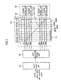
- Fig. 1 illustrates a system of a related art plasma display panel with a resolution of 640x480.
- the related art plasma display panel is provided with a panel having 640x3 address electrode lines R1, G1, R2, G2, B2, ---, R639, G639, B639, R640, G640, B640, 480 scan electrode lines S1, S2, ---, S480 vertical to the address electrode lines, and sustain electrode lines 14 of the same number as the scan electrode lines, an address electrode driving unit 50 for applying data pulses to the address electrode line 17, a scan electrode driving unit 30 for applying scan pulses and sustain pulses to the scan electrode line 14, a sustain electrode driving unit 60 for applying the sustain pulses to the sustain electrode line 14, and a microcomputer 20 for controlling the address electrode driving unit 50, the scan electrode driving unit 30, and the sustain electrode driving unit 60.
- a microcomputer 20 for controlling the address electrode driving unit 50, the scan electrode driving unit 30, and the sustain electrode driving unit 60.
- the panel is provided with an upper substrate 10 and a lower substrate 10', both of which are bonded together facing each other.
- Fig. 2b illustrates a section of the panel illustrated in Fig. 2a, with the lower substrate turned an angle of 90° with reference to an axis vertical to a substrate plane for convenience of explanation.
- the upper substrate 10 is provided with successive sets of the scan electrode and the sustain electrode, a dielectric layer coated on the upper substrate having the scan electrodes and the sustain electrodes formed thereon, and a protection film coated on the dielectric layer.
- the lower electrode 10' is provided with the address electrode formed to cross the scan electrodes and the sustain electrodes, and a lower dielectric layer 18 coated on the lower substrate having the address electrode formed thereon.
- each of the address lines 17 is formed continued on the lower substrate 10', and, as shown in Fig. 2a, the partition wall 19 separates adjacent address electrode lines.
- the address electrode lines are formed such that one set composed of adjacent three address electrode lines R1, G1, B1 forms one pixel.
- the one set of three address electrode lines 17 are adapted to be applied of data pulses for R(Red), G(Green), and B(Blue) video signals, respectively.
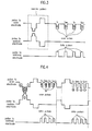
- the scan electrode lines S1, S2, S3, ---, S480, 14 and 14' and the sustain electrode lines 15 and 15' are formed to cross the address electrode lines 17 on the upper substrate 10 disposed to face the lower substrate 10', for being applied of sustain pulses as shown in Fig. 3.
- the sustain pulses applied to the scan electrode lines and the sustain electrode lines have opposite phases and the same frequencies.
- the microcomputer 20 receives a video signal and a clock signal and the like, and controls the address electrode driving unit 50, the scan electrode driving unit 30, and the sustain electrode driving unit 60 to realize an image of the video signal on the panel.
- the address driving unit 50 synchronous to the scan pulses, applies data pulses for the video data from the microcomputer to all address electrode lines 17 on the same time.
- the address electrode driving unit 50 receives the video data, and provides data pulses for selective discharge ofthe discharge cells.
- the data pulses for application to the address electrode lines 17 are illustrated in Fig. 3.
- the scan electrode driving unit 30 applies scan pulses to the scan electrode lines S1, S2, ---, S480 in succession in response to a control signal from the microcomputer 20 while the scan electrode driving unit 30 applies sustain pulses to all the scan electrode lines S1, S2, ---, S480.
- the control signal applied in this instance is in general called a 'BLANK' signal.
- the scan electrode driving unit 30 provides no scan pulses when the control signal is '0', and provides the scan pulses when the control signal is '1'.
- the sustain pulses and the scan pulses applied to the scan electrode lines S1, S2, ---, S480 is illustrated in Fig. 3.
- the sustain electrode driving unit 60 applies sustain pluses to all of the sustain electrode lines 15 on the same time.
- the sustain pulses applied to the sustain electrode lines has a phase opposite to a phase of the sustain pulses applied to the scan electrode lines 14.
- the plasma display panel is driven by discharges occurred among the electrodes, which is divided into a reset discharge period in which each of the discharge cells in the plasma display panel are initialized in response to the pulses applied to each electrode, an address discharge period in which each of the discharge cells are scanned line by line selectively, and a sustain discharge period in which a discharge in the discharge cell scanned during the address discharge period is sustained.
- the plasma display panel may be either a selective erasure method or a selective write method depending on characters of the discharge cell scanning in the address discharge period.
- the scan electrode lines 14 are applied of scan pluses in succession for one cycle of the sustain pulses.
- the address electrode driving unit 50 applies data pulses to the address electrode line 17 connected to the discharge cell to be discharge according to the video data provided from the microcomputer 20.
- a discharge is induced in the discharge cell of the discharge cells connected to the scan electrode lines 14 applied of the scan pulses at a portion crossing the address electrode line 17 applied of data pulses, to generate a wall charge at a surface of the dielectric layer on the scan electrode 14 and 14' and the sustain electrode 15 and 15' in the discharge cell.
- the address electrode driving unit 50 applies data pulses determining discharge of the discharge cells connected to the one scan electrode line 14 on the same time according to the video data of one line amount provided form the microcomputer 20. For example, if it is intended to form white on all pixels connected to the one scan electrode line 14, data pulses are provided to all address electrode lines 17, to cause discharge in all the discharge cells on the one line. In this instance, it is impossible to apply scan pulses to all the scan electrode lines 14 for one cycle of the sustain pulses.
- the related art plasma display panel is provided with the scan electrode driving unit 30 having many driving IC's each connected to about 40 to 120 scan electrode lines 14. And, the related art plasma display panel has a scan pulse application interval set therein such that approx. 4 data pulses are applied for one cycle of the sustain pulses.
- the sustain pulses, the scan pulses, and the data pulses respectively applied during the reset discharge period, the address discharge period, and the sustain discharge period have waveforms as illustrated in Fig. 3.
- Write pulses are applied to the scan electrodes 14 and 14', added to the sustain pulses. Then, a voltage from the write pulse and the sustain pulse to the sustain electrode 15 and 15' induces a discharge in a discharge region between the sustain electrodes 14 and 14' and the scan electrodes 15 and 15'. Because a voltage between the scan pulse for the scan electrodes and the sustain pulse for the sustain electrodes is higher than the discharge initiation voltage. As a result, a wall charge is induced on the dielectric layer 11 on the sustain electrodes and the scan electrodes. As shown in Fig. 4, the scan electrode lines 14 are applied of scan pulses in succession for one cycle of the sustain pulses.
- the address electrode driving unit 50 applies data pulses to the address electrode 17 connected to the discharge cell to be discharged according to the video data provided from the microcomputer 90.
- a discharge is induced in the discharge cell of the discharge cells connected to the scan electrode lines 14 applied of the scan pulses at a portion crossing the address electrodes 17 applied of data pulses, to erase a wall charge formed at the dielectric layers on the scan electrode 14 and 14' and the sustain electrode 15 and 15' in the discharge cell. That is, while one scan pulse is applied to one scan electrode line 14, the address electrode driving unit 50 applies data pulses determining discharge of the discharge cells connected to the one scan electrode line 14 on the same time according to the video data of one line amount provided form the microcomputer 20.
- data pulses are not provided to all address electrode lines 17 in the address electrode driving unit 50 in a plasma display panel of the selective erasure method.
- data pulses are provided to all address electrode lines 17. That is, in view of forming a portion of an image in one discharge cell, the selective write method induces a discharge in the discharge cell by the data pulses, and the selective erasure method stops a discharge in the discharge cell by the data pulses.
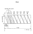
- a sub-field method illustrated in Fig. 5.
- one image displayed by the selective write method or the selective erasure method is set as one sub-field, and a number of the sub-fields are overlapped by controlling the scan electrode driving unit 30, the sustain electrode driving unith60, and the address electrode driving unit 50, to form one complete frame.
- this sub-field method it is required to gather a number of sub-fields in succession to form one frame, of which number is the same with a number of bits of gradation of the image.
- the number of sub-fields formed according to the sub-field method is also 8.
- a voltage come from one bit of digital video signal is applied to all cell in the plasma display panel, to form a first sub-field in which all cells have the same luminances.
- a voltage come from the next bit of digital video signal is applied, to form a second sub-field in which all cells have the same luminances, again.
- the luminances of the discharge cells in the first sub-field are the same and the luminances of the discharge cells in the second sub-field are the same, the luminances of the first, and second sub-fields are not the same.
- sub-fields each formed by the one bit of video signal there are a most significant sub-field by a most significant bit that has the highest luminance, a least significant sub-field by a least significant bit that has the lowest luminance, and a number of sub-fields by intermediate bits between the most significant bit and the least significant bit.
- one frame of image with 8 gradation is composed of an overlap of a first sub-field by the most significant bit, an eighth sub-field by the least significant bit, and a second, a third, a fourth, a fifth, and a sixth sub-fields of which luminances are differentiated by the six intermediate bits.
- such eight sub-fields are overlapped, to form one frame of perfect image by the residual image effect of a human eye.
- Fig. 6 illustrates a four-division sub-field driving system in which the scan electrode driving unit has four division
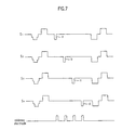
- Fig. 7 illustrates scan pulses, sustain pulses, and data pulse in the selective erasure method in driving the four-division plasma display panel illustrated in Fig. 6.
- a first scan pulse 'a' illustrated in Fig. 7 is applied to a first scan electrode line S1
- a second scan pulse 'b' is applied to an 121st scan electrode line S121
- a third scan pulse 'c' is applied to a 241st scan electrode line S241
- a fourth scan pulse 'd' is applied to a 361st scan electrode line S361, for addressing the discharge cells on each of the lines.
- the first scan pulse 'a' is applied to a second scan electrode line S2
- a second scan pulse 'b' is applied to an 122nd scan electrode line S122
- a third scan pulse 'c' is applied to a 242nd scan electrode line S242
- a fourth scan pulse 'd' is applied to a 362nd scan electrode line S362, for addressing the discharge cells on each of the lines.
- the four-division sub-field driving system illustrated in Fig. 6 proceeds the addressing until an 120 th addressing discharge interval is finished, to address the discharge cells on all the scan electrode lines S1, S2, ---, S480.
- the address driving unit provides a data pulse which determines a discharge of the discharge cells connected to the scan electrode line to which a scan pulse is applied every time the scan pulse is applied in each address discharge interval.
- the address driving unit applies a data pulse which determines a discharge of the discharge cells connected to the first scan electrode line S1.
- the address driving unit applies a data pulse which determines a discharge of the discharge cells connected to the 121st scan electrode line S121.
- the address driving unit applies a data pulse of the video data for the discharge cells connected to the first scan electrode line to the address electrode lines, a data pulse of the video data for the discharge cells connected to the 121st scan electrode line to the address electrode lines, a data pulse of the video data for the discharge cells connected to the 241st scan electrode line to the address electrode lines, a data pulse of the video data for the discharge cells connected to the 361st scan electrode line to the address electrode lines, a data pulse of the video data for the discharge cells connected to the second scan electrode line to the address electrode lines, a data pulse of the video data for the discharge cells connected to the 122nd scan electrode line to the address electrode lines, a data pulse of the video data for the discharge cells connected to the 242nd scan electrode line to the address electrode lines, and a data pulse of the video data for the discharge cells connected to the 362nd scan electrode line to the address electrode lines.
- the first scan pulse 'a' is applied to the first scan pulse electrode line S1 for forming a sub-field image of the next bit, and so on in the sequence as shown in Table 1.
- the four-division sub-field driving system forms an image on the plasma display by applying the scan pulses to the scan electrode lines as shown in Table 1.
- the four-division sub-field driving system shows flickers of image at an interface portion L1 of a region P1 in which the scan electrode line is addressed by the first scan pulse and a region P2 in which the scan electrode line is addressed by the second scan pulse, at an interface portion L2 of a region P2 in which the scan electrode line is addressed by the second scan pulse and a region P3 in which the scan electrode line is addressed by the third scan pulse, and at an interface portion L3 of a region P3 in which the scan electrode line is addressed by the third scan pulse and a region P4 in which the scan electrode line is addressed by the four scan pulse.
- the flickers are occurred because the discharge cells connected to the scan electrode line at each interface portion may have bits of grades different from each other, with different discharge states. For example, while the discharge cells connected to the 120 th scan electrode line S120 form an image of 7 bit grade, the discharge cells connected to the 121 st scan electrode line S121 may form an image of 6 bit grade.
- an image of the plasma display panel driven by the plasma display panel driving method illustrated in Fig. 6 generates contour noises, failing to provide a stable image to users.
- the contour noise is a disturbance of image an watcher can notice when the watcher watches the image while the watcher moves a point of view. This contour noise is occurred frequently in a moving picture with a gradation. The contour noise is occurred because the watcher happens to feel as if an image grade is formed irregularly at observing different sub-fields in one frame during the watcher watches the image while the watcher moves a point of view.
- the watcher may sense a sub-field image totally different from the sub-field image formed on the upper portion.
- the watcher feels like flickering of the image.
- preferred embodiments of the present invention are directed to circuits and methods for driving a plasma display panel that substantially obviate one or more of the problems of the prior art.
- certain preferred embodiments provide circuit and method for driving a plasma display panel which can reduce flickers and contour noises occurred in a plasma display panel image, to form a stable image.
- a method for driving a plasma display panel which includes the step of scanning a plurality of driving regions which are divisions of the plasma display panel on the same time.
- a method for driving a plasma display panel including the steps of (1) applying first scan pulses to a first driving block, which is any one of the driving blocks, in every given driving cycle starting from a first scan electrode line to (n)th scan electrode line in succession, and (2) applying second scan pulses each having a given application time difference from the application time of the first scan pulse to a second driving block adjacent to the first driving block starting from (m)th scan line to a first scan line in a reverse sequence to the first scan pulses.
- the second scan pulse is applied to a scan electrode line in the first driving block and the first scan pulse is applied to a scan electrode line in the second driving block in every given cycle. That is, an application sequence of the scan pulses applied to the first driving block and the second driving block is changed in turn in every given cycle.
- circuit for driving a plasma display panel including a panel unit having a plurality of scan electrode line and a plurality of sustain electrode lines, both arranged in parallel to each other, a plurality of address electrode lines arrange to cross the scan electrode line, with a discharge cell formed at every cross of the scan electrode lines and the address electrode lines, a plurality of driving circuit for applying driving signals different from one another to groups of scan electrode lines of a given number, a common circuit unit for applying driving signals to the sustain electrode lines, and a control unit for applying control signals to different driving units.
- the plasma display panel to which a method for driving a plasma display panel embodying the invention is applied has a plurality of driving blocks.
- a first scan pulse is applied to scan electrode lines in a first driving block which may be any one of the plurality of driving blocks in succession starting from a first scan line to a last scan line
- a second scan pulse is applied to scan electrode lines in a second driving block adjacent to the first driving block starting from a last scan line to a first scan line in succession such that an application of the second scan pulse has a given time difference from an application of the first scan pulse.
- the first, and second scan pulses have different application time points within identical sustain pulses.
- the scan pulses are applied to a driving block not at fixed time points within sustain pulses, but at time points varied with given cycles. There can be various embodiments of the present invention depending on application cycles and sequences of the different scan pulses to each driving block.
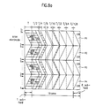
- an application time point of the scan pulse to each driving block is changed in a sequence whenever a sub-field is changed. That is, provided that the first scan pulse 'a' is applied to the first driving block P1 and, within the same sustain pulse cycle, a second scan pulse 'b' is applied to the second driving block P2 firstly, to form an (n)th sub-field image, in turn, the second scan pulse 'b' is applied to the first driving block P1 and, within the same sustain pulse cycle, the first scan pulse 'a' is applied to the second driving block P2 secondly, to form (n+1)th sub-field image.
- the first scan pulse 'a' is applied to the first driving block P1 and the second scan pulse 'b' is applied to the second driving block within the same sustain pulse cycle, to form an (n+2)th sub-field image. If there are equal to, or more than three driving blocks in the first embodiment of the present invention, the application time points of the scan pulses applied to different driving blocks respectively are changed in a sequence whenever the sub-field is changed.
- the first scan pulse is applied to the first driving block, the second pulse to the second driving block, and the third scan pulse to the third driving block, all within the same sustain pulse cycle firstly, to form an (n)th sub-field image
- the first scan pulse is applied to the second driving block, the second scan pulse to the third driving block, and the third scan pulse to the first driving block, all within the same sustain pulse cycle secondly, to form an (n+1)st sub-field image.
- the first scan pulse is applied to the third driving block, the second scan pulse to the first driving block, and the third scan pulse to the second driving block, all within the same sustain pulse cycle thirdly, to form an (n+2)nd sub-field image.
- the first scan pulse is applied to the first driving block, the second pulse to the second driving block, the third scan pulse to the third driving block, and the fourth scan pulse to the fourth driving block, all within the same sustain pulse cycle, to form an (n)th sub-field image firstly
- the first scan pulse is applied to the second driving block, the second pulse to the third driving block, the third scan pulse to the fourth driving block, and the fourth scan pulse to the first driving block, all within the same sustain pulse cycle, to form an (n+1)st sub-field image secondly
- the first scan pulse is applied to the third driving block, the second pulse to the fourth driving block, the third scan pulse to the first driving block, and the fourth scan pulse to the second driving block, all within the same sustain pulse cycle, to form an(n+2)nd sub-field image thirdly
- the first scan pulse is applied to the fourth driving block, the second pulse to the first driving block, the third scan pulse to the second driving block, and the fourth scan pulse to the fourth driving block, all within the same sustain pulse cycle, to form an(n+
- the driving blocks in the first embodiment plasma display panel of the present invention preferably has the same number of scan electrode lines.
- an application of the first embodiment method of the present invention may be extended such that the application time point of the scan pulse is changed in sequence whenever one set of sub-fields are changed instead of one sub-field.
- an application time point of the scan pulse applied to each driving block is changed in a sequence for every cycle of the sustain pulse. That is, provided that the first scan pulse is applied to the first driving block and, within the same sustain pulse cycle, a second scan pulse is applied to the second driving block to form an (n)th sub-field image in a first cycle of the sustain pulse, the second scan pulse is applied to the first driving block and, within the same sustain pulse cycle, the first scan pulse is applied to the second driving block to form (n+1)th sub-field image in a second cycle of the sustain pulse.
- the first scan pulse is applied to the first driving block and the second scan pulse is applied to the second driving block within the same sustain pulse cycle, to form an (n+2)th sub-field image in a third cycle of the sustain pulse.
- the application time points of the scan pulses applied to different driving blocks respectively are changed in a sequence in every sustain pulse cycle.
- the first scan pulse is applied to the first driving block, the second pulse to the second driving block, and the third scan pulse to the third driving block, all within the same sustain pulse cycle to form an (n)th sub-field image in the first cycle of the sustain pulse
- the first scan pulse is applied to the second driving block, the second scan pulse to the third driving block, and the third scan pulse to the first driving block, all within the same sustain pulse cycle, to form an (n+1)st sub-field image the second cycle of the sustain pulse.
- the first scan pulse is applied to the third driving block, the second scan pulse to the first driving block, and the third scan pulse to the second driving block, all within the same sustain pulse cycle, to form an (n+2)nd sub-field image in the third cycle of the sustain pulse.
- the first scan pulse is applied to the first driving block, the second pulse to the second driving block, the third scan pulse to the third driving block, and the fourth scan pulse to the fourth driving block, all within the same sustain pulse cycle, to form an (n)th sub-field image in the first cycle of the sustain pulse
- the first scan pulse is applied to the second driving block, the second pulse to the third driving block, the third scan pulse to the fourth driving block, and the fourth scan pulse to the first driving block, all within the same sustain pulse cycle, to form an (n+1)st sub-field image in the second cycle of the sustain pulse
- the first scan pulse is applied to the third driving block, the second pulse to the fourth driving block, the third scan pulse to the first driving block, and the fourth scan pulse to the second driving block, all within the same sustain pulse cycle, to form an (n+2)nd sub-field image in the third cycle of the sustain pulse
- the first scan pulse is applied to the fourth driving block
- the driving blocks in the first embodiment plasma display panel of the present invention preferably has the same number of scan electrode lines.
- an application of the second embodiment method of the present invention may be extended such that the application time point of the scan pulse is changed in sequence in every set of cycles of the sustain pulses instead of every sustain pulse.
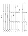
- the driving block has two, or more than two scan pulses applied thereto while a sequence of the application is changed in turn in every given driving cycle. If, within one cycle of the sustain pulse, the first scan pulse 'a' is applied to the first driving block P1 at an (x)th scan electrode line and the second scan pulse 'b' is applied to the second driving block P2 at a (y)th scan electrode line firstly, the third scan pulse 'c' is applied to the first driving block P1 at (x+1)st scan electrode line before the second scan pulse 'b' is applied to the second driving block P2 at a (y-1)st scan electrode line secondly.
- the third scan pulse 'c' is applied to the first driving block P1 at the (x)th scan electrode line having the first scan pulse 'a' applied thereto and the first scan pulse 'a' is applied to the first driving block at (x+1)st scan electrode line.
- the first scan pulse 'a' is applied to the first driving block P1 at the (x)th scan electrode line
- the second scan pulse 'b' is applied to the first driving block P1 at the (x-1)st scan electrode line
- the third scan pulse 'c' is applied to the second driving hlock P2 at the (y)th scan electrode line.
- numbers of the scan electrode lines in the first and second driving blocks P1 and P2 should be at a ratio of 2:1.
- a ratio of numbers of the scan pulses applied to the first driving block P1 and the scan pulses applied to the second driving block is the same with the ratio of the numbers of the scan electrode lines in the first driving block P1 and the scan electrode lines in the second driving block P2.
- the ratio of the numbers of the scan electrode lines in the first and second driving blocks P1 and P2 may be greater than 3:1. As shown in Fig.
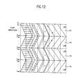
- the first, second, and third scan pulses 'a', 'b', and 'c' are applied to the first driving block P1 at an (x)th, (x+1)st, and (x+2)nd scan electrode lines respectively, during which cycle the fourth scan pulse 'd' is applied to the second driving block P2 at a (y)th scan electrode line. Then, a sequence ofapplication of the scan pulses to the driving blocks is changed in turn in every given driving cycle.
- first, second, and third scan pulses 'a', 'b', and 'c' are applied to the first driving block P1 at the (x)th, (x+1)st, and (x+2)nd scan electrode lines in succession respectively and the fourth scan pulse 'd' is applied to the second driving block P2 at the (y)th scan electrode line, to form an (n)th frame
- the second, third, and fourth scan pulses 'b', 'c', and 'd' are applied to the first driving block P1 at the (x)th, (x+1)st, and (x+2)nd scan electrode lines in succession respectively and the first scan pulse 'a' is applied to the second driving block P2 at the (y)th scan electrode line, to form an (n+1)th frame.
- the third, fourth, and first scan pulses 'c', 'd', and 'a' are applied to the first driving block P1 at the (x)th, (x+1)st, and (x+2)nd scan electrode lines in succession respectively and the second scan pulse 'b' is applied to the second driving block P2 at the (y)th scan electrode line, to form an (n+2)th frame.
- the sequence of the scan pulse application may be changed in turn in either every frame as explained, or every set of frames instead of every frame, or every sub-field, or every set of sub-fields.
- the ratio of the numbers of the scan pulses applied to the first and second driving blocks P1 and P2 is an integer, the ratio may not be an integer.
- the sequence of the scan pulse application may be changed in turn in every integer time of the sustain pulse cycle. That is, if the first, second, and third scan pulses 'a', 'b', and 'c' are applied to the first driving block P1 at a first to third scan electrode lines respectively in succession and the fourth scan pulse 'd' is applied to the second driving block P2 at a first scan electrode line firstly, the fourth, first, and second scan pulses 'd', 'a', and 'b' are applied to the first driving block P1 at a fourth to sixth scan electrode lines in succession respectively and the third scan pulse 'c' is applied to the second driving block P2 at a second scan electrode line secondly.
- the third, fourth, and first scan pulses 'c', 'd', and 'a' are applied to the first driving block P1 at a seventh to ninth scan electrode lines in succession respectively and the second scan pulse 'b' is applied to the second driving block P2 at a third scan electrode line thirdly and the second, third, and fourth scan pulses 'b', 'c', and 'd' are applied to the first driving block P1 at a tenth to twelfth scan electrode lines in succession respectively and the first scan pulse 'a' is applied to the second driving block P2 at a fourth scan electrode line fourthly.
- scan pulses for forming sub-fields different from each other are applied to one driving block with a given time difference.
- the first scan pulse 'a' for an (n)th sub-field image is applied to the first driving block P1 at an (x)th scan electrode line and the first scan pulse 'a" for an (n+1)st sub-field image is applied to the first driving block P1 at a first scan electrode line within the same sustain pulse cycle.
- the second scan pulse 'b' for an (n)th sub-field image is applied to the second driving block P2 at an (y)th scan electrode line and the first scan pulse 'b" for an (n+1)st sub-field image is applied to the second driving block P2 at a first scan electrode line within the same sustain pulse cycle.
- Fig. 13 illustrates a circuit for driving a plasma display panel in accordance with a preferred embodiment of the present invention.
- the circuit for driving a plasma display panel in accordance with a preferred embodiment of the present invention includes a panel unit 400 for displaying an image, a scan driving unit 100 for applying a sustain pulse and a scan pulse to the panel unit 400, a common circuit unit 300 for applying a sustain pulse having a phase opposite to the sustain pulse to the scan driving unit 100, an address driving unit 200 for applying a video data to the panel unit 400, and a controlling unit 500 for applying control signals to different units 100, 200 and 300.
- the panel unit 400 has a plurality of scan electrode lines 111, 121, 131 and 141 and a plurality of sustain electrode lines 301, both arranged in parallel, and address electrode lines 201 arranged to cross the scan electrode lines 111, 121, 131 and 141. There is a discharge cell at every cross of each of the scan electrode lines 111, 121, 131 and 141 and the address electrode lines 201.
- the panel unit 400 is operative in response to the scan pulse and the sustain pulse from the scan driving unit 100 and the sustain pulse from the common circuit unit 300.
- the scan driving unit 100 applies the scan pulses and the sustain pulses, both different from one another respectively, to blocks P1, P2, P3 and P4 of the scan electrode lines 111, 121, 131 and 141.
- each of a first to a fourth scan drivers 110, 120, 130 and 140 applies scan pulses, such as first scan pulse 'a' and a second scan pulse 'b', to respective scan electrode lines 111, 121, 131 and 141.
- the common circuit unit 300 sustains applies a sustain pulse to the sustain electrode lines to sustain discharge in the discharge cells between the scan electrode lines 111, 121, 131 and 141 and the sustain electrode lines 301.
- the control unit 500 latches scan data and applies control signals to respective scan drivers 110, 120, 130 and 140, to control application of the scan pulses to the scan electrode lines 111, 121, 131 and 141.
- a scan data for a (j+1)th second scan pulse 'b' to be applied to the second driving block P2 is adapted to be latched at the control unit during a time between application time points of a (j)th first scan pulse 'a' and a (j+1)th first scan pulse 'a' to the first driving block P1.
- the method for driving a plasma display panel of the present invention has an advantage of preventing an occurrence of flicker because interfaces between driving blocks are continuous with respect to time.
- the method and the circuit for driving a PDP embodying the invention can provide a PDP having a resolution better than an HDTV because intervals of scan pulse application to adjacent lines are short.
Landscapes
- Engineering & Computer Science (AREA)
- Physics & Mathematics (AREA)
- Computer Hardware Design (AREA)
- General Physics & Mathematics (AREA)
- Theoretical Computer Science (AREA)
- Power Engineering (AREA)
- Plasma & Fusion (AREA)
- Control Of Indicators Other Than Cathode Ray Tubes (AREA)
- Control Of Gas Discharge Display Tubes (AREA)
Applications Claiming Priority (6)
| Application Number | Priority Date | Filing Date | Title |
|---|---|---|---|
| KR5804498 | 1998-02-24 | ||
| KR1019980005844A KR100523861B1 (ko) | 1998-02-24 | 1998-02-24 | 플라즈마 표시장치의 구동방법 |
| KR1019980009006A KR100489446B1 (ko) | 1998-03-17 | 1998-03-17 | 플라즈마 표시패널 구동방법 |
| KR9000698 | 1998-03-17 | ||
| KR1019980047018A KR100323690B1 (ko) | 1998-11-03 | 1998-11-03 | 플라즈마 디스플레이 패널의 구동방법 |
| KR4701898 | 1998-11-03 |
Publications (2)
| Publication Number | Publication Date |
|---|---|
| EP0938073A2 true EP0938073A2 (fr) | 1999-08-25 |
| EP0938073A3 EP0938073A3 (fr) | 2000-08-02 |
Family
ID=27349686
Family Applications (1)
| Application Number | Title | Priority Date | Filing Date |
|---|---|---|---|
| EP99301271A Withdrawn EP0938073A3 (fr) | 1998-02-24 | 1999-02-22 | Circuit et dispositif de commande d'un panneau d'affichage à plasma |
Country Status (4)
| Country | Link |
|---|---|
| US (1) | US6340960B1 (fr) |
| EP (1) | EP0938073A3 (fr) |
| JP (2) | JPH11288251A (fr) |
| CN (1) | CN1133146C (fr) |
Cited By (4)
| Publication number | Priority date | Publication date | Assignee | Title |
|---|---|---|---|---|
| US6492776B2 (en) | 2000-04-20 | 2002-12-10 | James C. Rutherford | Method for driving a plasma display panel |
| EP1191510A3 (fr) * | 2000-09-21 | 2003-05-28 | Samsung SDI Co., Ltd. | Méthode de commande d'un panneau d'affichage à plasma |
| EP1696461A1 (fr) * | 2005-01-13 | 2006-08-30 | LG Electronics, Inc. | Panneau d'affichage à plasma |
| WO2007126937A3 (fr) * | 2006-03-28 | 2009-02-26 | David W Stebbings | système et procédé pour l'identification de supports cinétiques dans des lecteurs et des enregistreurs sans accès Internet |
Families Citing this family (27)
| Publication number | Priority date | Publication date | Assignee | Title |
|---|---|---|---|---|
| US6407506B1 (en) * | 1999-04-02 | 2002-06-18 | Hitachi, Ltd. | Display apparatus, display method and control-drive circuit for display apparatus |
| US7456808B1 (en) | 1999-04-26 | 2008-11-25 | Imaging Systems Technology | Images on a display |
| US7911414B1 (en) | 2000-01-19 | 2011-03-22 | Imaging Systems Technology | Method for addressing a plasma display panel |
| JP3560143B2 (ja) * | 2000-02-28 | 2004-09-02 | 日本電気株式会社 | プラズマディスプレイパネルの駆動方法及び駆動回路 |
| JP3758930B2 (ja) * | 2000-03-17 | 2006-03-22 | 三星エスディアイ株式会社 | 画像表示装置及びその駆動方法 |
| JP4253422B2 (ja) * | 2000-06-05 | 2009-04-15 | パイオニア株式会社 | プラズマディスプレイパネルの駆動方法 |
| EP1172787A1 (fr) * | 2000-07-13 | 2002-01-16 | Deutsche Thomson-Brandt Gmbh | Commande de niveaux de gris sur un écran d'affichage du type matriciel |
| KR100421667B1 (ko) * | 2001-03-07 | 2004-03-10 | 엘지전자 주식회사 | 플라즈마 디스플레이 패널의 구동방법 및 장치 |
| JP4695770B2 (ja) * | 2001-03-28 | 2011-06-08 | パナソニック株式会社 | プラズマディスプレイ装置 |
| CN1623177A (zh) * | 2001-05-30 | 2005-06-01 | 皇家菲利浦电子有限公司 | 用于驱动显示屏的方法和设备 |
| US6744674B1 (en) * | 2003-03-13 | 2004-06-01 | Advanced Micro Devices, Inc. | Circuit for fast and accurate memory read operations |
| KR100477602B1 (ko) * | 2002-04-22 | 2005-03-18 | 엘지전자 주식회사 | 플라즈마 디스플레이 패널의 구동방법 |
| KR100917323B1 (ko) * | 2002-10-30 | 2009-09-11 | 엘지디스플레이 주식회사 | 강유전성 액정표시장치와 그 구동방법 |
| KR100490542B1 (ko) * | 2002-11-26 | 2005-05-17 | 삼성에스디아이 주식회사 | 어드레스기간과 유지기간의 혼합 방식으로 동작하는패널구동방법 및 그 장치 |
| KR100472515B1 (ko) * | 2002-12-03 | 2005-03-10 | 삼성에스디아이 주식회사 | 어드레스기간과 유지기간의 혼합 방식으로 계조성을표현하는 패널구동방법 및 그 장치 |
| JP4327097B2 (ja) * | 2002-12-10 | 2009-09-09 | オリオン ピーディーピー カンパニー リミテッド | マルチスクリーン型プラズマディスプレイ装置 |
| US8305301B1 (en) | 2003-02-04 | 2012-11-06 | Imaging Systems Technology | Gamma correction |
| US8289233B1 (en) | 2003-02-04 | 2012-10-16 | Imaging Systems Technology | Error diffusion |
| KR100542233B1 (ko) * | 2003-10-16 | 2006-01-10 | 삼성에스디아이 주식회사 | 플라즈마 디스플레이 패널의 구동 방법 및 플라즈마 표시장치 |
| KR100820632B1 (ko) * | 2004-08-27 | 2008-04-10 | 엘지전자 주식회사 | 플라즈마 디스플레이 패널 구동 방법 |
| US20060181487A1 (en) * | 2005-02-14 | 2006-08-17 | Lg Electronics Inc. | Plasma display apparatus and driving method thereof |
| JP2007017802A (ja) * | 2005-07-08 | 2007-01-25 | Toshiba Corp | 画像データ処理装置 |
| KR100670184B1 (ko) * | 2005-07-18 | 2007-01-16 | 삼성에스디아이 주식회사 | 플라즈마 표시 장치 및 그 구동 방법 |
| JPWO2007108111A1 (ja) * | 2006-03-22 | 2009-07-30 | 篠田プラズマ株式会社 | 3電極面放電型表示装置の駆動方法、およびその駆動方法により駆動させられる表示装置 |
| US8248328B1 (en) | 2007-05-10 | 2012-08-21 | Imaging Systems Technology | Plasma-shell PDP with artifact reduction |
| JP2011145531A (ja) * | 2010-01-15 | 2011-07-28 | Sony Corp | 表示装置およびその駆動方法ならびに電子機器 |
| KR102275709B1 (ko) | 2015-03-13 | 2021-07-09 | 삼성전자주식회사 | 게이트 드라이버, 디스플레이 구동 회로 및 디스플레이 장치 |
Citations (2)
| Publication number | Priority date | Publication date | Assignee | Title |
|---|---|---|---|---|
| JPH0764508A (ja) * | 1993-08-30 | 1995-03-10 | Fujitsu General Ltd | 表示パネルの駆動方法およびその装置 |
| JPH08305320A (ja) * | 1995-04-28 | 1996-11-22 | Nec Corp | プラズマディスプレイパネルの駆動方法 |
Family Cites Families (14)
| Publication number | Priority date | Publication date | Assignee | Title |
|---|---|---|---|---|
| JPH01233492A (ja) | 1988-03-15 | 1989-09-19 | Fujitsu Ltd | 平板型表示装置の駆動方法 |
| JPH02291597A (ja) | 1989-05-02 | 1990-12-03 | Fujitsu Ltd | ガス放電パネルの駆動方式 |
| JP2898027B2 (ja) | 1989-10-09 | 1999-05-31 | 株式会社日立製作所 | 表示装置及び表示装置の走査方法 |
| JPH0418594A (ja) | 1990-05-12 | 1992-01-22 | Mitsubishi Electric Corp | プラズマディスプレイ表示装置 |
| JP2932686B2 (ja) * | 1990-11-28 | 1999-08-09 | 日本電気株式会社 | プラズマディスプレイパネルの駆動方法 |
| JPH064039A (ja) | 1992-06-19 | 1994-01-14 | Fujitsu Ltd | Ac型プラズマディスプレイパネル及びその駆動回路 |
| JPH06282242A (ja) * | 1993-03-25 | 1994-10-07 | Pioneer Electron Corp | ガス放電パネルの駆動方法 |
| US5684499A (en) * | 1993-11-29 | 1997-11-04 | Nec Corporation | Method of driving plasma display panel having improved operational margin |
| JPH07261700A (ja) | 1994-03-25 | 1995-10-13 | Matsushita Electron Corp | 画像表示放電管駆動方法 |
| JPH0930054A (ja) | 1995-07-18 | 1997-02-04 | Fuji Xerox Co Ltd | バーコード印刷装置 |
| JP3233023B2 (ja) * | 1996-06-18 | 2001-11-26 | 三菱電機株式会社 | プラズマディスプレイ及びその駆動方法 |
| JP3524323B2 (ja) * | 1996-10-04 | 2004-05-10 | パイオニア株式会社 | プラズマディスプレイパネルの駆動装置 |
| JPH10260655A (ja) | 1997-03-19 | 1998-09-29 | Matsushita Electric Ind Co Ltd | Ac型プラズマディスプレイパネルの駆動方法 |
| JPH1165486A (ja) | 1997-08-18 | 1999-03-05 | Nec Corp | プラズマディスプレイパネルおよびその駆動方法 |
-
1999
- 1999-02-22 EP EP99301271A patent/EP0938073A3/fr not_active Withdrawn
- 1999-02-22 US US09/253,730 patent/US6340960B1/en not_active Expired - Lifetime
- 1999-02-24 CN CN99103427A patent/CN1133146C/zh not_active Expired - Fee Related
- 1999-02-24 JP JP11047255A patent/JPH11288251A/ja active Pending
-
2005
- 2005-05-02 JP JP2005134652A patent/JP2005266821A/ja active Pending
Patent Citations (2)
| Publication number | Priority date | Publication date | Assignee | Title |
|---|---|---|---|---|
| JPH0764508A (ja) * | 1993-08-30 | 1995-03-10 | Fujitsu General Ltd | 表示パネルの駆動方法およびその装置 |
| JPH08305320A (ja) * | 1995-04-28 | 1996-11-22 | Nec Corp | プラズマディスプレイパネルの駆動方法 |
Cited By (6)
| Publication number | Priority date | Publication date | Assignee | Title |
|---|---|---|---|---|
| US6492776B2 (en) | 2000-04-20 | 2002-12-10 | James C. Rutherford | Method for driving a plasma display panel |
| EP1191510A3 (fr) * | 2000-09-21 | 2003-05-28 | Samsung SDI Co., Ltd. | Méthode de commande d'un panneau d'affichage à plasma |
| US6677921B2 (en) | 2000-09-21 | 2004-01-13 | Samsung Sdi Co., Ltd. | Method of driving plasma display panel |
| EP1696461A1 (fr) * | 2005-01-13 | 2006-08-30 | LG Electronics, Inc. | Panneau d'affichage à plasma |
| US7859485B2 (en) | 2005-01-13 | 2010-12-28 | Lg Electronics Inc. | Plasma display panel |
| WO2007126937A3 (fr) * | 2006-03-28 | 2009-02-26 | David W Stebbings | système et procédé pour l'identification de supports cinétiques dans des lecteurs et des enregistreurs sans accès Internet |
Also Published As
| Publication number | Publication date |
|---|---|
| CN1133146C (zh) | 2003-12-31 |
| CN1233038A (zh) | 1999-10-27 |
| US6340960B1 (en) | 2002-01-22 |
| JP2005266821A (ja) | 2005-09-29 |
| JPH11288251A (ja) | 1999-10-19 |
| EP0938073A3 (fr) | 2000-08-02 |
Similar Documents
| Publication | Publication Date | Title |
|---|---|---|
| US6340960B1 (en) | Circuit and method for driving plasma display panel | |
| JP2903984B2 (ja) | ディスプレイ装置の駆動方法 | |
| US6057815A (en) | Driver circuit for AC-memory plasma display panel | |
| JPH1124628A (ja) | プラズマディスプレイパネルの階調表示方法 | |
| JP2001154634A (ja) | プラズマ表示パネルの駆動方法 | |
| JPH08254965A (ja) | 表示装置の階調表示方法 | |
| JPH11352941A (ja) | 光変調器 | |
| JPH1092323A (ja) | 表示パネル及びパネル型表示装置 | |
| US7385570B2 (en) | Method and apparatus for driving panel by performing mixed address period and sustain period | |
| KR100706004B1 (ko) | 플라즈마 표시장치 및 플라즈마 표시장치를 사용하기 위한구동방법 | |
| US6600463B2 (en) | Method of driving a plasma display panel | |
| KR100458690B1 (ko) | 표시장치 및 화상표시방법 | |
| JP2003066897A (ja) | プラズマディスプレイパネル表示装置とその駆動方法 | |
| KR100700858B1 (ko) | 플라즈마 디스플레이 패널의 구동방법 및 플라즈마디스플레이장치 | |
| US6472826B2 (en) | Method of driving plasma display panel and a plasma display device using the method | |
| JP3272898B2 (ja) | 液晶表示装置 | |
| KR100267216B1 (ko) | 플라즈마디스플레이패널의구동장치 | |
| US7408532B2 (en) | Plasma display device and drive method for use in plasma display device | |
| KR100313911B1 (ko) | 플라즈마 디스플레이 패널의 구동방법 | |
| US6587085B2 (en) | Method of a driving plasma display panel | |
| KR100251148B1 (ko) | 3전극 면방전 플라즈마 디스플레이 패널의 구동방법 | |
| KR100310687B1 (ko) | 플라즈마 표시 패널의 구동방법 | |
| US20050083252A1 (en) | Plasma display panel device using sub-field mode and method of driving the same | |
| US20010011973A1 (en) | Method and apparatus for driving plasma display panel | |
| KR19990008956A (ko) | 피디피의 구동방법 |
Legal Events
| Date | Code | Title | Description |
|---|---|---|---|
| PUAI | Public reference made under article 153(3) epc to a published international application that has entered the european phase |
Free format text: ORIGINAL CODE: 0009012 |
|
| 17P | Request for examination filed |
Effective date: 19990308 |
|
| AK | Designated contracting states |
Kind code of ref document: A2 Designated state(s): DE FR GB NL |
|
| AX | Request for extension of the european patent |
Free format text: AL;LT;LV;MK;RO;SI |
|
| RIN1 | Information on inventor provided before grant (corrected) |
Inventor name: LEE, NAM KYU Inventor name: LEE, JAE HYUCK Inventor name: CHUNG, MOON SHICK, LG ELECTRONICS DORMITORY A-217 Inventor name: SONG, YOUNG BOK, LG ELECTRONICS DORMITORY A-404 |
|
| PUAL | Search report despatched |
Free format text: ORIGINAL CODE: 0009013 |
|
| AK | Designated contracting states |
Kind code of ref document: A3 Designated state(s): AT BE CH CY DE DK ES FI FR GB GR IE IT LI LU MC NL PT SE |
|
| AX | Request for extension of the european patent |
Free format text: AL;LT;LV;MK;RO;SI |
|
| AKX | Designation fees paid |
Free format text: DE FR GB NL |
|
| 17Q | First examination report despatched |
Effective date: 20071022 |
|
| STAA | Information on the status of an ep patent application or granted ep patent |
Free format text: STATUS: THE APPLICATION IS DEEMED TO BE WITHDRAWN |
|
| 18D | Application deemed to be withdrawn |
Effective date: 20150708 |