EP0939437A2 - Planarisation des couches d'interconnexion - Google Patents
Planarisation des couches d'interconnexion Download PDFInfo
- Publication number
- EP0939437A2 EP0939437A2 EP99103548A EP99103548A EP0939437A2 EP 0939437 A2 EP0939437 A2 EP 0939437A2 EP 99103548 A EP99103548 A EP 99103548A EP 99103548 A EP99103548 A EP 99103548A EP 0939437 A2 EP0939437 A2 EP 0939437A2
- Authority
- EP
- European Patent Office
- Prior art keywords
- barrier metal
- metal layer
- electrically conductive
- recess
- layer
- Prior art date
- Legal status (The legal status is an assumption and is not a legal conclusion. Google has not performed a legal analysis and makes no representation as to the accuracy of the status listed.)
- Withdrawn
Links
Images




Classifications
-
- H—ELECTRICITY
- H10—SEMICONDUCTOR DEVICES; ELECTRIC SOLID-STATE DEVICES NOT OTHERWISE PROVIDED FOR
- H10P—GENERIC PROCESSES OR APPARATUS FOR THE MANUFACTURE OR TREATMENT OF DEVICES COVERED BY CLASS H10
- H10P14/00—Formation of materials, e.g. in the shape of layers or pillars
- H10P14/40—Formation of materials, e.g. in the shape of layers or pillars of conductive or resistive materials
- H10P14/46—Formation of materials, e.g. in the shape of layers or pillars of conductive or resistive materials using a liquid
-
- H—ELECTRICITY
- H10—SEMICONDUCTOR DEVICES; ELECTRIC SOLID-STATE DEVICES NOT OTHERWISE PROVIDED FOR
- H10W—GENERIC PACKAGES, INTERCONNECTIONS, CONNECTORS OR OTHER CONSTRUCTIONAL DETAILS OF DEVICES COVERED BY CLASS H10
- H10W20/00—Interconnections in chips, wafers or substrates
- H10W20/01—Manufacture or treatment
- H10W20/031—Manufacture or treatment of conductive parts of the interconnections
- H10W20/032—Manufacture or treatment of conductive parts of the interconnections of conductive barrier, adhesion or liner layers
- H10W20/033—Manufacture or treatment of conductive parts of the interconnections of conductive barrier, adhesion or liner layers in openings in dielectrics
-
- H—ELECTRICITY
- H10—SEMICONDUCTOR DEVICES; ELECTRIC SOLID-STATE DEVICES NOT OTHERWISE PROVIDED FOR
- H10P—GENERIC PROCESSES OR APPARATUS FOR THE MANUFACTURE OR TREATMENT OF DEVICES COVERED BY CLASS H10
- H10P52/00—Grinding, lapping or polishing of wafers, substrates or parts of devices
- H10P52/40—Chemomechanical polishing [CMP]
- H10P52/403—Chemomechanical polishing [CMP] of conductive or resistive materials
-
- H—ELECTRICITY
- H10—SEMICONDUCTOR DEVICES; ELECTRIC SOLID-STATE DEVICES NOT OTHERWISE PROVIDED FOR
- H10W—GENERIC PACKAGES, INTERCONNECTIONS, CONNECTORS OR OTHER CONSTRUCTIONAL DETAILS OF DEVICES COVERED BY CLASS H10
- H10W10/00—Isolation regions in semiconductor bodies between components of integrated devices
- H10W10/01—Manufacture or treatment
- H10W10/041—Manufacture or treatment of isolation regions comprising polycrystalline semiconductor materials
-
- H—ELECTRICITY
- H10—SEMICONDUCTOR DEVICES; ELECTRIC SOLID-STATE DEVICES NOT OTHERWISE PROVIDED FOR
- H10W—GENERIC PACKAGES, INTERCONNECTIONS, CONNECTORS OR OTHER CONSTRUCTIONAL DETAILS OF DEVICES COVERED BY CLASS H10
- H10W10/00—Isolation regions in semiconductor bodies between components of integrated devices
- H10W10/40—Isolation regions comprising polycrystalline semiconductor materials
-
- H—ELECTRICITY
- H10—SEMICONDUCTOR DEVICES; ELECTRIC SOLID-STATE DEVICES NOT OTHERWISE PROVIDED FOR
- H10W—GENERIC PACKAGES, INTERCONNECTIONS, CONNECTORS OR OTHER CONSTRUCTIONAL DETAILS OF DEVICES COVERED BY CLASS H10
- H10W20/00—Interconnections in chips, wafers or substrates
- H10W20/01—Manufacture or treatment
- H10W20/031—Manufacture or treatment of conductive parts of the interconnections
- H10W20/062—Manufacture or treatment of conductive parts of the interconnections by smoothing of conductive parts, e.g. by planarisation
-
- H—ELECTRICITY
- H10—SEMICONDUCTOR DEVICES; ELECTRIC SOLID-STATE DEVICES NOT OTHERWISE PROVIDED FOR
- H10P—GENERIC PROCESSES OR APPARATUS FOR THE MANUFACTURE OR TREATMENT OF DEVICES COVERED BY CLASS H10
- H10P14/00—Formation of materials, e.g. in the shape of layers or pillars
- H10P14/40—Formation of materials, e.g. in the shape of layers or pillars of conductive or resistive materials
- H10P14/42—Formation of materials, e.g. in the shape of layers or pillars of conductive or resistive materials using a gas or vapour
- H10P14/44—Physical vapour deposition [PVD]
Definitions
- the invention relates to a semiconductor device including an electrically conductive layer formed by chemical mechanical polishing, and further to a method of fabricating such a semiconductor device.
- a wiring layer As a semiconductor device has been more highly integrated recently, a wiring layer is required to have a smaller resistance. To this end, a wiring layer has been generally composed of copper (Cu) having a high resistance to electro-migration (EM).
- Cu copper
- EM electro-migration
- an electrically conducive film is formed of copper.
- Such an electrically conductive film is formed by the steps of forming a recess or a contact hole with an insulating layer in accordance with a wiring pattern, filling the recess or contact hole with a copper layer, and removing an unnecessary portion of the copper layer by chemical mechanical polishing (hereinafter, referred to simply as "CMP").
- an electrically conductive layer is composed of copper
- a barrier metal layer such as a TiN layer between an insulating layer and the electrically conductive layer. This is because if an electrically conductive layer composed of copper is formed directly on an insulating film such as a silicon dioxide film, copper readily diffuses among silicon dioxide molecules to thereby establish a deep level in silicon semiconductor, which would shorten lifetime of minority carriers.
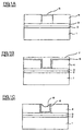
- Figs. 1A to 1C illustrates respective steps of the method suggested in the Publication.
- a silicon dioxide layer 2 acting as an underlying insulating layer, and a tungsten wiring layer 3 are deposited on a silicon substrate 1. Then, a silicon dioxide layer 4 is deposited on the tungsten wiring layer 3 by plasma-enhanced chemical vapor deposition (PCVD) by a thickness of 600 nm.
- PCVD plasma-enhanced chemical vapor deposition
- a photoresist film (not illustrated) having a thickness of 0.6 ⁇ m is formed on the silicon dioxide layer 4, and thereafter, is patterned by means of i-ray having a wavelength of 365 nm.
- the silicon dioxide layer 4 is etched using the thus patterned photoresist film as a mask, to thereby form a contact hole 5 throughout the silicon dioxide layer 4.
- the contact hole 5 has a width of 0.5 ⁇ m and a depth of 1 ⁇ m, which means that the contact hole 5 has an aspect ratio of 2, and reaches the tungsten wiring layer 3.
- a TiN layer 6 is deposited over the silicon dioxide layer 4 and the exposed tungsten wiring layer 3 by chemical vapor deposition (hereinafter, referred to simply as "CVD") or sputtering.
- CVD chemical vapor deposition
- sputtering is inferior to CVD with respect to coverage ability for covering steps therewith, but is superior to CVD with respect to barrier performance.
- a copper layer 7 is formed entirely over the TiN layer 6 so that the contact hole 5 is filled with the copper layer 7.
- the above-mentioned problem is accompanied with a problem that the copper contact electrode 8 is recessed, as illustrated in Fig. 1C, as a result of removal of the unnecessary portions of copper layer 7 and the TiN layer 6 by CMP.
- the reason is as follows. Copper has a polishing rate significantly greater than a polishing rate of TiN. Hence, when the TiN layer 6 formed on the silicon dioxide layer 4 is removed by CMP, the copper layer 7 is polished too excessively while the TiN layer 6 is being polished. As a result, the copper layer 7 is recessed at a center thereof in the shape of a dish (hereinafter, a recess formed in the center of the copper contact electrode 8 is referred to as "dishing").
- the copper contact electrode 8 Since it would be necessary to carry out over-etching to some degree in order to almost completely remove the unnecessary portion of the TiN layer 6, it would be unavoidable for the copper contact electrode 8 to have a remarkable dishing. Dishing would be more remarkable in an electrically conductive layer having a greater length.
- Japanese Unexamined Patent Publication No. 9-306915 has suggested a method of removing a defect generated in a copper layer while the copper layer is being polished by CMP.
- the suggested method includes the steps of forming a groove with a silicon dioxide film formed on a semiconductor substrate, depositing a barrier metal composed of TiN by sputtering, depositing a copper film on the barrier metal, filling the groove with the copper film by reflow, removing an unnecessary portion of the copper film by CMP so that the groove remains filled with the copper film, and applying heat treatment to the product in hydrogen atmosphere to thereby eliminate defects having been generated in the copper layer.
- the present invention accomplishes the above-mentioned objects by increasing a polishing rate at which a barrier metal layer is polished by CMP.
- a semiconductor device including (a) a semiconductor substrate, (b) an insulating layer formed on the semiconductor substrate and formed with at least one recess or hole, (c) a barrier metal layer covering an inner wall of the recess or hole therewith, and (d) at least one electrically conductive layer formed on the barrier metal layer to fill the recess or hole therewith, characterized by that assuming that X indicates a maximum depth of a recess in an electrically conductive layer having a longest wiring length, and that Y indicates a thickness of the electrically conductive layer having a longest wiring length, a ratio of Y to X (X/Y) is set equal to or smaller than 0.1.
- dishing is generated at a surface of an electrically conductive film when an unnecessary portion of a barrier metal film is removed by CMP.
- dishing generated at a surface of an electrically conductive film is defined as a ratio of Y to X (X/Y) where X indicates a depth of dishing, and Y indicates a thickness of an electrically conductive film.
- the ratio X/Y is greater in an electrically conductive film having a greater wiring length.
- the present invention provides a semiconductor device in which an electrically conductive film having a longest wiring length is designed to have the ratio X/Y equal to or smaller than 0.1. It is preferable that the ratio of Y to X is equal to or smaller than 0.05.
- the semiconductor device can be fabricated, as mentioned later, by decreasing a density of a barrier metal layer, which is accomplished, for instance, by optimizing sputtering conditions for forming a barrier metal layer.
- a semiconductor device including (a) a semiconductor substrate, (b) an insulating layer formed on the semiconductor substrate and formed with at least one recess or hole, (c) a barrier metal layer covering an inner wall of the recess or hole therewith, and (d) at least one electrically conductive layer formed on the barrier metal layer to fill the recess or hole therewith, characterized by that a dishing index defined as a resistance to dishing is set equal to or greater than 0.4.
- a degree of dishing in an electrically conductive film is dependent on a lot of factors including (a) materials of which a barrier metal layer and an electrically conductive film are composed, (b)thicknesses of a barrier metal layer and an electrically conductive film, (c) a configuration of a contact hole which is to be filled with copper, (d) a degree of over-etching, and (e) polishing conditions of CMP.
- factors (b)to (e) are subject to other restrictions in a process of fabricating a semiconductor device.
- the present invention uses a parameter called dishing index indicating a resistance to dishing in a barrier metal layer and an electrically conductive film, and defines a preferable range of the dishing index.
- the dishing index is a parameter which is defined with a combination of a barrier metal layer and an electrically conductive layer, and is dependent on materials of which those layers are composed, and a process by which those layers are formed.
- the dishing index is detailed.
- the dishing index indicative a resistance to dishing is measured in an experiment where materials of which a barrier metal layer and an electrically conductive layer are composed, and conditions for forming those layers are standardized in such a manner that dishing is readily generated.
- an insulating layer 4 is formed with a groove 5 by which an electrically conductive film having a relatively great length is formed.
- a refractory metal film and an electrically conductive film are formed over the groove 5 in accordance with the steps illustrated in Figs. 1A to 1C.
- unnecessary portions of those films are removed by CMP.
- dishing index is measured by estimating the thus generated dishing.
- the groove 5 is designed to have a length of 4 mm, a width of 1 mm, and a depth of 500 nm, and the barrier metal layer is designed to have a thickness of 50 nm.
- CMP is conducted at r.p.m. of 25 under a pressure of 2 psi.
- Polishing slurry is alumina particle suspension containing hydrogen peroxide (H 2 O 2 ) therein.
- H 2 O 2 hydrogen peroxide
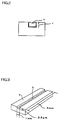
- the dishing index is defined as a depth X (see Fig. 2) of the thus generated dishing in the center of the electrically conductive film, divided by a thickness Y (see Fig. 2) of 500 nm of the electrically conductive film.
- the dishing index indicates a resistance to dishing obtained when an electrically conductive film and a barrier metal layer constituting a semiconductor device under test are applied to the groove 5 illustrated in Fig. 3.
- the dishing index indicates a resistance to dishing of a sample where an electrically conductive film and a barrier metal film are applied to the groove 5 illustrated in Fig. 3 with both materials of which those films are composed and processes of forming those films being kept unchanged and only configuration of those films being varied.
- Table 1 shows a relation between the dishing index and a degree of dishing generated when a contact hole or a wiring layer has been actually formed.
- the dishing index is set equal to or smaller than 0.4, more preferably 0.2, and most preferably 0.1.
- the present invention defines a range of the dishing index in the above-mentioned standpoint.
- dishing index corresponding to 10% dishing means dishing index measured when the electrically conductive layer listed in the left column is caused to have 10% dishing. For instance, if the dishing index is set equal to 0.1, a semiconductor device including a buried electrically conductive layer formed in a contact hole having a size of 1 ⁇ m ⁇ 1 ⁇ m would have a degree of dishing at 10%. For another instance, a semiconductor device including a buried electrically conductive layer formed in a groove having a wiring length of 15 ⁇ m and a wiring width of 35 ⁇ m would have a degree of dishing at 10%.
- a semiconductor device including (a) a semiconductor substrate, (b) an insulating layer formed on the semiconductor substrate and formed with at least one recess, (c) a barrier metal layer covering an inner wall of the recess therewith, the barrier metal layer having a first polishing rate at which the barrier metal layer is polished by chemical mechanical polishing, and (d) at least one electrically conductive layer formed on the barrier metal layer to fill the recess therewith, the electrically conductive layer having a second polishing rate at which the electrically conductive layer is polished by chemical mechanical polishing, characterized by that the first polishing rate is set at least 2.6 ⁇ 10 -2 times greater than the second polishing rate.
- the present invention prevents generation of dishing by increasing a polishing rate of an electrically conductive film to thereby increase a ratio of a polishing rate of an electrically conductive film to a polishing rate of a barrier metal layer. Dishing can be reduced down to a level at which no practical problem is caused, by setting a ratio of a polishing rate at which a barrier metal layer is polished by CMP to a polishing rate at which an electrically conductive film is polished by CMP, equal to or greater than 2.6 ⁇ 10 -2 , more preferably 5.3 ⁇ 10 -2 .
- a barrier metal film composed of refractory material such as refractory metal nitride has a significantly smaller polishing rate than that of an electrically conductive film composed of copper. Hence, the above-mentioned ratio is usually equal to or smaller than 1.
- a semiconductor device including (a) a semiconductor substrate, (b) an insulating layer formed on the semiconductor substrate and formed with at least one recess, (c) a barrier metal layer covering an inner wall of the recess therewith, and (d) at least one electrically conductive layer formed on the barrier metal layer to fill the recess therewith, characterized by that a polishing rate at which the barrier metal layer is polished by chemical mechanical polishing is set equal to or greater than 40 angstroms per minute.
- the present invention prevents generation of dishing by increasing a polishing rate of an electrically conductive film to thereby increase a ratio of a polishing rate of an electrically conductive film to a polishing rate of a barrier metal layer. Dishing can be reduced down to a level at which no practical problem is caused, by setting a polishing rate at which a barrier metal layer is polished by CMP equal to or greater than 40 angstroms per minute, more preferably, 80 angstroms per minute.
- a barrier metal film composed of refractory material such as refractory metal nitride has a significantly smaller polishing rate than a polishing rate of an electrically conductive film composed of copper (1000 angstroms per minute).
- a semiconductor device including (a) a semiconductor substrate, (b) an insulating layer formed on the semiconductor substrate and formed with at least one recess, (c) a barrier metal layer covering an inner wall of the recess therewith, and (d) at least one electrically conductive layer formed on the barrier metal layer to fill the recess therewith, characterized by that the barrier metal layer is designed to have a compressive stress equal to or smaller than 3 ⁇ 10 8 dyne/cm 2 .
- a compressive stress in a barrier metal layer can be measured based on a dimension and a curvature of a substrate.
- a semiconductor device including (a) a semiconductor substrate, (b) an insulating layer formed on the semiconductor substrate and formed with at least one recess, (c) a barrier metal layer covering an inner wall of the recess therewith, and (d) at least one electrically conductive layer formed on the barrier metal layer to fill the recess therewith, characterized by that the barrier metal layer is designed to have a density equal to or smaller than 6 ⁇ 10 22 atoms/cm 3 .
- a barrier metal layer in the semiconductor device is designed to have a smaller density than a density of a barrier metal layer in a conventional semiconductor device, it is possible to increase a polishing rate at which a barrier metal layer is polished by CMP, resulting in reduction in dishing.
- a density of a barrier metal layer in the semiconductor device has no lower limit, unless performances of the barrier metal layer are not deteriorated.
- a density of the barrier metal layer is calculated based on a thickness and a weight thereof.
- the electrically conductive layer is composed of copper or copper compounds
- the barrier metal layer is composed of refractive metal nitride.
- Refractive metal nitride of which the barrier metal layer is composed may be selected from WN, TiN, or TaN, among which TiN or TaN is more preferably used.
- a method of fabricating a semiconductor device including the steps of (a) forming an insulating film on a semiconductor substrate, (b) forming a recess with the insulating film, (c) forming a barrier metal layer over an inner wall of the recess by sputtering, (d) forming an electrically conductive layer over the barrier metal layer to fill the recess therewith, and over the insulating film, and (e) removing the electrically conductive layer by chemical mechanical polishing in such a manner that the recess remains filled with the electrically conductive layer, characterized by that the sputtering is carried out under at least one of the following conditions:
- the barrier metal layer is formed by sputtering for enhancing barrier ability.
- sputtering conditions it is possible to increase a polishing rate of a barrier metal layer to thereby reduce dishing.
- Conditions for doing so are the above-mentioned ones (A) to (C).
- the method is required to meet with at least one of the conditions (A) to (C). If the method meets with two or three conditions, it would be possible to further increase a polishing rate of a barrier metal layer to thereby further reduce dishing.
- a sputtering pressure is set equal to or greater than 3 mTorr and/or setting a temperature of a substrate at which the sputtering is to be carried out to be equal to or greater than 200 degrees centigrade.
- a sputtering power is equal to or smaller than 4.5 kW and/or setting a temperature of a substrate at which the sputtering is to be carried out to be equal to or greater than 200 degrees centigrade.
- a temperature of the substrate is set equal to or greater than 360 degrees centigrade, it would be possible to further increase a polishing rate of a barrier metal layer by setting a sputtering power to be equal to or smaller than 4.5 kW and/or setting a sputtering pressure to be equal to or greater than 3 mTorr.
- a method of fabricating a semiconductor device including the steps of (a) forming an insulating film on a semiconductor substrate, (b) forming a recess with the insulating film, (c) forming a barrier metal layer over an inner wall of the recess by sputtering, (d) forming an electrically conductive layer over the barrier metal layer to fill the recess therewith, and over the insulating film, and (e) removing the electrically conductive layer by chemical mechanical polishing in such a manner that the recess remains filled with the electrically conductive layer, characterized by that the sputtering is carried out under following conditions: W/P ⁇ 0.4 and T ⁇ 200 wherein W indicates a sputtering power in the unit of kW, P indicates a sputtering pressure in the unit of mTorr, and T indicates a substrate temperature when the sputtering is carried out, in the unit of degrees centigrade.
- a ratio of W/P is set equal to or smaller than 0.4, more preferably, 0.3.
- the reason why the ratio of W/P is set equal to or smaller than a certain constant is to reduce acceleration energy per a sputtered particle to thereby lower a density of a barrier metal layer. This is detailed later.
- a substrate is more advantageously kept at a higher temperature during sputtering.
- a substrate is kept preferably at 200 degrees centigrade, and more preferably at 300 degrees centigrade.
- the electrically conductive film is composed of copper or copper compounds, and the barrier metal layer is composed of TiN.
- the electrically conductive layer is composed of copper or copper compounds
- the barrier metal layer is composed of TaN
- the sputtering is carried out under following conditions: W/P ⁇ 0.35 and T ⁇ 200 wherein W indicates a sputtering power in the unit of kW, P indicates a sputtering pressure in the unit of mTorr, and T indicates a substrate temperature when the sputtering is carried out, in the unit of degrees centigrade.
- a ratio of W/P is set equal to or smaller than 0.35, more preferably, 0.3.
- a polishing rate is dependent on a density of a film to be polished, and becomes higher in a film having a smaller density.
- a density of a film formed by sputtering is dependent on sputtering power, sputtering pressure, and a temperature of a substrate during sputtering is being carried out. This is because a density of a film varies in dependence on acceleration energy to be applied to sputtered particles.
- a sputtered particle would have higher acceleration energy, and hence, there would be formed a film into which sputtered particles are incorporated in a higher density. As a result, the resultant film would have a higher density.
- each one of sputtered particles would have higher acceleration energy even when sputtering power is kept constant, resulting in an increase in a density of the film.
- the present invention reduces a degree of dishing by increasing a polishing rate at which a barrier metal layer is polished by CMP.
- the polishing rate can be increased by reducing a density of a barrier metal layer.
- reduction in a density of a barrier metal layer is accompanied with reduction in a compressive stress in a barrier metal layer.
- Fig. 4 shows a relation between a compressive stress in a barrier metal layer and a polishing rate at which a barrier metal layer is polished by CMP
- Fig. 5 shows a relation between a compressive stress in a barrier metal layer and a density of a barrier metal layer
- Fig. 6 shows a relation between a polishing rate at which a barrier metal layer is polished by CMP and dishing index. Table 2 shows those relations.
- the dishing index is necessary to be equal to or smaller than 0.4, more preferably 0.2, and most preferably 0.1, in view of Table 1.
- the dishing index can be designed to be equal to or smaller than 0.4, and hence, a degree of dishing can be reduced to a degree at which no practical problem is caused in a semiconductor device, by forming a barrier metal layer meeting with at least one of the above-mentioned conditions (a) to (d).
- Designing the dishing index to be equal to or smaller than 0.2 is equivalent to designing a ratio of a polishing rate of a barrier metal layer and a polishing rate of an electrically conductive film to be equal to or greater than 4.0 ⁇ 10 -2 , or designing a polishing rate of a barrier metal layer to be equal to or greater than 60 angstroms per minute.
- Designing the dishing index to be equal to or smaller than 0.1 is equivalent to designing a ratio of a polishing rate of a barrier metal layer and a polishing rate of an electrically conductive film to be equal to or greater than 5.3 ⁇ 10 -2 , or designing a polishing rate of a barrier metal layer to be equal to or greater than 80 angstroms per minute.
- a barrier metal layer is composed of TiN, and an electrically conductive film is composed of copper.
- Reduction in the dishing index is accomplished in the present invention by increasing a polishing rate at which a barrier metal layer is polished by CMP. This is because a principal factor for a polishing rate and a compressive stress is a density of a barrier metal layer.
- a density and a compressive stress of a barrier metal layer have no lower limit in principle, but actually have a lower limit based on performances of a sputtering apparatus. For instance, a compressive stress becomes lower and a density becomes smaller in lower sputtering power. However, if sputtering power were set equal to or smaller than 0.2 kW reproducibility provided by existing sputtering apparatuses would be deteriorated.
- a compressive stress becomes lower and a density becomes smaller in a higher sputtering pressure.
- a sputtering pressure is set too high, plasma is not generated with the result of inability of sputtering.
- Such a critical pressure at which sputtering cannot be carried out is dependent on apparatuses, and hence, it is necessary to know a pressure range in which sputtering can be carried out, for each of sputtering apparatuses.
- a substrate temperature has no upper limit in principle, but has actual upper limit dependent on performances of sputtering apparatuses.
- sputtering power may be decreased, or sputtering conditions may be optimized.
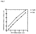
- Figs. 7 shows a relation between sputtering power and a compressive stress in a barrier metal layer
- Fig. 8 shows a relation between a sputtering pressure and a compressive stress in a barrier metal layer
- Fig. 9 shows a relation between a substrate temperature during sputtering and a compressive stress in a barrier metal layer.
- a compressive stress in a barrier metal layer has negative correlation with a polishing rate of a barrier metal layer
- a polishing rate of a barrier metal layer has negative correlation with the dishing index. Accordingly, a greater compressive stress indicates a greater dishing index.
- designing the dishing index equal to or smaller than 0.4 is equivalent to designing a compressive stress equal to or smaller than 3 ⁇ 10 8 dyne/cm 2 .
- sputtering condition meeting with the above-mentioned requirement is that sputtering power is equal to or smaller than 0.5 kW.
- the graph in Fig. 7 is based on measurements obtained when a sputtering pressure is equal to 3 mTorr and a substrate temperature is equal to 200 degrees centigrade.
- a compressive stress becomes lower in a higher sputtering pressure and/or at a higher substrate temperature. This is because Figs. 8 and 9 shows that a compressive stress becomes lower in a higher sputtering pressure and/or at a higher substrate temperature.
- a compressive stress can be further reduced by setting a sputtering pressure equal to or greater than 3 mTorr and/or by setting a substrate temperature equal to or greater than 200 degrees centigrade.
- a compressive stress is equal to or smaller than 3 ⁇ 10 8 dyne/cm 2 when a sputtering pressure is equal to or greater than 12 mTorr.
- the graph in Fig. 8 is based on measurements obtained when sputtering power is equal to 4.5 kW and a substrate temperature is equal to 200 degrees centigrade.
- a compressive stress can be further reduced by setting sputtering power equal to or smaller than 4.5 kW and/or by setting a substrate temperature equal to or greater than 200 degrees centigrade.
- a compressive stress is equal to or smaller than 3 ⁇ 10 8 dyne/cm 2 when a substrate temperature is equal to or greater than 450 degrees centigrade.
- the graph in Fig. 9 is based on measurements obtained when sputtering power is equal to 4.5 kW and a sputtering pressure is equal to 3 mTorr.
- a compressive stress can be further reduced by setting sputtering power equal to or smaller than 4.5 kW and/or by setting a sputtering pressure equal to or greater than 3 mTorr.
- a silicon dioxide layer 2 acting as an underlying insulating layer, and a tungsten wiring layer 3 were deposited in this order on a silicon substrate 1. Then, a silicon dioxide layer 4 was deposited on the tungsten wiring layer 3 by PCVD by a thickness of 600 nm.
- a photoresist film (not illustrated) having a thickness of 0.6 ⁇ m was formed on the silicon dioxide layer 4, and thereafter, was patterned by means of i-ray having a wavelength of 365 nm.
- the silicon dioxide layer 4 was etched using the thus patterned photoresist film as a mask, to thereby form a contact hole 5 throughout the silicon dioxide layer 4.
- the contact hole 5 had a width of 0.5 ⁇ m and a depth of 1 ⁇ m which means that the contact hole 5 has an aspect ratio of 2, and reached the tungsten wiring layer 3.
- a TiN layer 6 as a barrier metal layer was deposited over both the silicon dioxide layer 4 and the exposed tungsten wiring layer 3 by sputtering under the following sputtering conditions.
- the thus formed copper contact electrode 8 was estimated as to whether dishing was generated therein. The results are shown in Table 3. In Table 3, "NO” in the column titled “Dishing” means that dishing was not generated or a degree of dishing was equal to or smaller than 0.1 (10%) even though dishing was generated, and "YES” means that a degree of dishing was greater than 0.1 (10%).
- Example 2 was carried out in the same manner as Example 1 except that the TiN layer 6 was formed in the following sputtering conditions.
- Example 3 was carried out in the same manner as Example 1 except that the TiN layer 6 was formed in the following sputtering conditions.
- Example 4 was carried out in the same manner as Example 1 except that a barrier metal layer 6 was composed of TaN, and was deposited under the following sputtering conditions.
- Example 5 was carried out in the same manner as Example 1 except that a barrier metal layer 6 was composed of TaN, and was deposited under the following sputtering conditions.
- Reference 1 was carried out in the same manner as Example 1 except that the TiN layer 6 as a barrier metal layer was deposited under the following sputtering conditions.
- Reference 2 was carried out in the same manner as Example 1 except that a barrier metal layer 6 was composed of TaN, and was deposited under the following sputtering conditions.
- Examples 2 to 5 and References 1 to 2 were also estimated as to whether dishing was generated therein. The results are shown in Table 3.
- Barrier Metal Layer Sputtering Power [kW] Sputtering Pressure [mTorr] Sputtering Power / Sputtering Pressure Substrate Temp.[°C] Dishing
- Example 1 TiN 0.5 3 0.17 200 NO
- Example 2 TiN 4.5 12 0.38 200 NO
- Example 3 TiN 4.5 3 1.5 450 NO
- a silicon dioxide layer 2 acting as an underlying insulating layer, and a tungsten wiring layer 3 were deposited in this order on a silicon substrate 1. Then, a silicon dioxide layer 4 was deposited on the tungsten wiring layer 3 by PCVD by a thickness of 600 nm.
- a photoresist film (not illustrated) having a thickness of 0.6 ⁇ m was formed on the silicon dioxide layer 4, and thereafter, was patterned by means of i-ray having a wavelength of 365 nm.
- the silicon dioxide layer 4 was etched using the thus patterned photoresist film as a mask, to thereby form a contact hole 5 throughout the silicon dioxide layer 4.
- the contact hole 5 had a width of 0.18 ⁇ m and a length of 15 mm, and reached the tungsten wiring layer 3.
- a TiN layer 6 as a barrier metal layer was deposited over both the silicon dioxide layer 4 and the exposed tungsten wiring layer 3 by sputtering under the following sputtering conditions.
- the thus formed copper contact electrode 8 had a flat upper surface, which means that dishing was not generated.
- the present invention prevents generation of dishing, which in turn prevents electro-migration.
- the present invention prevents generation of dishing by increasing a polishing rate at which a barrier metal layer is polished by CMP, other fabrication conditions are not influenced.
Landscapes
- Internal Circuitry In Semiconductor Integrated Circuit Devices (AREA)
- Electrodes Of Semiconductors (AREA)
- Mechanical Treatment Of Semiconductor (AREA)
Applications Claiming Priority (2)
| Application Number | Priority Date | Filing Date | Title |
|---|---|---|---|
| JP4780498 | 1998-02-27 | ||
| JP04780498A JP3374901B2 (ja) | 1998-02-27 | 1998-02-27 | 半導体装置 |
Publications (2)
| Publication Number | Publication Date |
|---|---|
| EP0939437A2 true EP0939437A2 (fr) | 1999-09-01 |
| EP0939437A3 EP0939437A3 (fr) | 2003-03-05 |
Family
ID=12785565
Family Applications (1)
| Application Number | Title | Priority Date | Filing Date |
|---|---|---|---|
| EP99103548A Withdrawn EP0939437A3 (fr) | 1998-02-27 | 1999-02-24 | Planarisation des couches d'interconnexion |
Country Status (5)
| Country | Link |
|---|---|
| EP (1) | EP0939437A3 (fr) |
| JP (1) | JP3374901B2 (fr) |
| KR (1) | KR100403937B1 (fr) |
| CN (1) | CN1144285C (fr) |
| TW (1) | TW418463B (fr) |
Cited By (3)
| Publication number | Priority date | Publication date | Assignee | Title |
|---|---|---|---|---|
| WO2001091181A3 (fr) * | 2000-05-23 | 2002-07-11 | Applied Materials Inc | Materiaux de revetement |
| WO2002007198A3 (fr) * | 2000-07-18 | 2002-07-18 | Applied Materials Inc | Depot de films de tantale de faible contrainte |
| WO2006068741A3 (fr) * | 2004-12-22 | 2007-01-25 | 3M Innovative Properties Co | Articles de circuit electronique souple et procedes de fabrication afferents |
Families Citing this family (1)
| Publication number | Priority date | Publication date | Assignee | Title |
|---|---|---|---|---|
| JP4095731B2 (ja) * | 1998-11-09 | 2008-06-04 | 株式会社ルネサステクノロジ | 半導体装置の製造方法及び半導体装置 |
Family Cites Families (11)
| Publication number | Priority date | Publication date | Assignee | Title |
|---|---|---|---|---|
| US577095A (en) * | 1897-02-16 | Tor of benjamin hewitt | ||
| JPH0666287B2 (ja) * | 1988-07-25 | 1994-08-24 | 富士通株式会社 | 半導体装置の製造方法 |
| JP3407204B2 (ja) * | 1992-07-23 | 2003-05-19 | オリンパス光学工業株式会社 | 強誘電体集積回路及びその製造方法 |
| US5340370A (en) * | 1993-11-03 | 1994-08-23 | Intel Corporation | Slurries for chemical mechanical polishing |
| US5514908A (en) * | 1994-04-29 | 1996-05-07 | Sgs-Thomson Microelectronics, Inc. | Integrated circuit with a titanium nitride contact barrier having oxygen stuffed grain boundaries |
| JP3397501B2 (ja) * | 1994-07-12 | 2003-04-14 | 株式会社東芝 | 研磨剤および研磨方法 |
| JPH08162531A (ja) * | 1994-12-05 | 1996-06-21 | Sony Corp | 配線形成方法 |
| US5676587A (en) * | 1995-12-06 | 1997-10-14 | International Business Machines Corporation | Selective polish process for titanium, titanium nitride, tantalum and tantalum nitride |
| JP3487051B2 (ja) * | 1995-12-15 | 2004-01-13 | 松下電器産業株式会社 | 半導体装置の製造方法 |
| JPH1012729A (ja) * | 1996-06-27 | 1998-01-16 | Nec Corp | 半導体装置の製造方法 |
| US6139699A (en) * | 1997-05-27 | 2000-10-31 | Applied Materials, Inc. | Sputtering methods for depositing stress tunable tantalum and tantalum nitride films |
-
1998
- 1998-02-27 JP JP04780498A patent/JP3374901B2/ja not_active Expired - Fee Related
-
1999
- 1999-02-24 EP EP99103548A patent/EP0939437A3/fr not_active Withdrawn
- 1999-02-24 TW TW088102820A patent/TW418463B/zh not_active IP Right Cessation
- 1999-02-26 KR KR10-1999-0006594A patent/KR100403937B1/ko not_active Expired - Fee Related
- 1999-03-01 CN CNB991007875A patent/CN1144285C/zh not_active Expired - Fee Related
Cited By (4)
| Publication number | Priority date | Publication date | Assignee | Title |
|---|---|---|---|---|
| WO2001091181A3 (fr) * | 2000-05-23 | 2002-07-11 | Applied Materials Inc | Materiaux de revetement |
| US6528180B1 (en) | 2000-05-23 | 2003-03-04 | Applied Materials, Inc. | Liner materials |
| WO2002007198A3 (fr) * | 2000-07-18 | 2002-07-18 | Applied Materials Inc | Depot de films de tantale de faible contrainte |
| WO2006068741A3 (fr) * | 2004-12-22 | 2007-01-25 | 3M Innovative Properties Co | Articles de circuit electronique souple et procedes de fabrication afferents |
Also Published As
| Publication number | Publication date |
|---|---|
| JPH11251431A (ja) | 1999-09-17 |
| KR100403937B1 (ko) | 2003-11-01 |
| JP3374901B2 (ja) | 2003-02-10 |
| TW418463B (en) | 2001-01-11 |
| EP0939437A3 (fr) | 2003-03-05 |
| CN1144285C (zh) | 2004-03-31 |
| CN1227413A (zh) | 1999-09-01 |
| KR19990072998A (ko) | 1999-09-27 |
Similar Documents
| Publication | Publication Date | Title |
|---|---|---|
| US5854140A (en) | Method of making an aluminum contact | |
| US6077773A (en) | Damascene process for reduced feature size | |
| US6342448B1 (en) | Method of fabricating barrier adhesion to low-k dielectric layers in a copper damascene process | |
| US5736462A (en) | Method of etching back layer on substrate | |
| US6200897B1 (en) | Method for manufacturing even dielectric layer | |
| US6316329B1 (en) | Forming a trench mask comprising a DLC and ASH protecting layer | |
| US5968847A (en) | Process for copper etch back | |
| US8389410B2 (en) | Chemical mechanical polishing method | |
| US6507081B2 (en) | In-situ silicon nitride and silicon based oxide deposition with graded interface for damascene application | |
| US7208404B2 (en) | Method to reduce Rs pattern dependence effect | |
| US6611060B1 (en) | Semiconductor device having a damascene type wiring layer | |
| US6017803A (en) | Method to prevent dishing in chemical mechanical polishing | |
| KR20000023003A (ko) | 반도체 기판의 표면 평탄화 처리 방법 및 절연층에서의 전도 플러그 생성 처리 방법 | |
| US6645863B2 (en) | Method of manufacturing semiconductor device and semiconductor device | |
| US6265315B1 (en) | Method for improving chemical/mechanical polish uniformity over rough topography for semiconductor integrated circuits | |
| US20040253809A1 (en) | Forming a semiconductor structure using a combination of planarizing methods and electropolishing | |
| US6066550A (en) | Method of improving selectivity between silicon nitride and silicon oxide | |
| KR100350111B1 (ko) | 반도체 장치의 배선 및 이의 제조 방법 | |
| EP0939437A2 (fr) | Planarisation des couches d'interconnexion | |
| US5930671A (en) | CVD titanium silicide for contract hole plugs | |
| US6746954B2 (en) | Method of reworking tungsten particle contaminated semiconductor wafers | |
| JP2001118928A (ja) | 集積回路の製造方法 | |
| US7098515B1 (en) | Semiconductor chip with borderless contact that avoids well leakage | |
| US20020168846A1 (en) | Method for forming buried interconnect | |
| US6831016B2 (en) | Method to prevent electrical shorts between adjacent metal lines |
Legal Events
| Date | Code | Title | Description |
|---|---|---|---|
| PUAI | Public reference made under article 153(3) epc to a published international application that has entered the european phase |
Free format text: ORIGINAL CODE: 0009012 |
|
| AK | Designated contracting states |
Kind code of ref document: A2 Designated state(s): AT BE CH CY DE DK ES FI FR GB GR IE IT LI LU MC NL PT SE |
|
| AX | Request for extension of the european patent |
Free format text: AL;LT;LV;MK;RO;SI |
|
| PUAL | Search report despatched |
Free format text: ORIGINAL CODE: 0009013 |
|
| AK | Designated contracting states |
Kind code of ref document: A3 Designated state(s): AT BE CH CY DE DK ES FI FR GB GR IE IT LI LU MC NL PT SE Designated state(s): AT BE CH CY DE DK ES FI FR GB GR IE IT LI LU MC NL PT SE |
|
| AX | Request for extension of the european patent |
Extension state: AL LT LV MK RO SI |
|
| 17P | Request for examination filed |
Effective date: 20030123 |
|
| RAP1 | Party data changed (applicant data changed or rights of an application transferred) |
Owner name: NEC ELECTRONICS CORPORATION |
|
| STAA | Information on the status of an ep patent application or granted ep patent |
Free format text: STATUS: THE APPLICATION HAS BEEN WITHDRAWN |
|
| 17Q | First examination report despatched |
Effective date: 20030714 |
|
| 18W | Application withdrawn |
Effective date: 20030806 |