EP0939937B1 - Elektronische Karte - Google Patents
Elektronische Karte Download PDFInfo
- Publication number
- EP0939937B1 EP0939937B1 EP97938323A EP97938323A EP0939937B1 EP 0939937 B1 EP0939937 B1 EP 0939937B1 EP 97938323 A EP97938323 A EP 97938323A EP 97938323 A EP97938323 A EP 97938323A EP 0939937 B1 EP0939937 B1 EP 0939937B1
- Authority
- EP
- European Patent Office
- Prior art keywords
- card
- shield
- tabs
- shields
- connector
- Prior art date
- Legal status (The legal status is an assumption and is not a legal conclusion. Google has not performed a legal analysis and makes no representation as to the accuracy of the status listed.)
- Expired - Lifetime
Links
Images








Classifications
-
- H—ELECTRICITY
- H05—ELECTRIC TECHNIQUES NOT OTHERWISE PROVIDED FOR
- H05K—PRINTED CIRCUITS; CASINGS OR CONSTRUCTIONAL DETAILS OF ELECTRIC APPARATUS; MANUFACTURE OF ASSEMBLAGES OF ELECTRICAL COMPONENTS
- H05K5/00—Casings, cabinets or drawers for electric apparatus
- H05K5/02—Details
- H05K5/0256—Details of interchangeable modules or receptacles therefor, e.g. cartridge mechanisms
- H05K5/026—Details of interchangeable modules or receptacles therefor, e.g. cartridge mechanisms having standardized interfaces
- H05K5/0265—Details of interchangeable modules or receptacles therefor, e.g. cartridge mechanisms having standardized interfaces of PCMCIA type
- H05K5/0269—Card housings therefor, e.g. covers, frames, PCB
-
- G—PHYSICS
- G06—COMPUTING OR CALCULATING; COUNTING
- G06K—GRAPHICAL DATA READING; PRESENTATION OF DATA; RECORD CARRIERS; HANDLING RECORD CARRIERS
- G06K19/00—Record carriers for use with machines and with at least a part designed to carry digital markings
- G06K19/06—Record carriers for use with machines and with at least a part designed to carry digital markings characterised by the kind of the digital marking, e.g. shape, nature, code
- G06K19/067—Record carriers with conductive marks, printed circuits or semiconductor circuit elements, e.g. credit or identity cards also with resonating or responding marks without active components
- G06K19/07—Record carriers with conductive marks, printed circuits or semiconductor circuit elements, e.g. credit or identity cards also with resonating or responding marks without active components with integrated circuit chips
- G06K19/077—Constructional details, e.g. mounting of circuits in the carrier
-
- G—PHYSICS
- G06—COMPUTING OR CALCULATING; COUNTING
- G06K—GRAPHICAL DATA READING; PRESENTATION OF DATA; RECORD CARRIERS; HANDLING RECORD CARRIERS
- G06K19/00—Record carriers for use with machines and with at least a part designed to carry digital markings
- G06K19/06—Record carriers for use with machines and with at least a part designed to carry digital markings characterised by the kind of the digital marking, e.g. shape, nature, code
- G06K19/067—Record carriers with conductive marks, printed circuits or semiconductor circuit elements, e.g. credit or identity cards also with resonating or responding marks without active components
- G06K19/07—Record carriers with conductive marks, printed circuits or semiconductor circuit elements, e.g. credit or identity cards also with resonating or responding marks without active components with integrated circuit chips
- G06K19/077—Constructional details, e.g. mounting of circuits in the carrier
- G06K19/0772—Physical layout of the record carrier
- G06K19/07735—Physical layout of the record carrier the record carrier comprising means for protecting against electrostatic discharge
Definitions
- the present invention relates to electronic cards and more particularly to exterior shells for such cards.
- PCMCIA Personal Computer Memory Card International Association
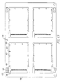
- US 5,548,483 B discloses an electronic card comprising a printed circuit board assembly interposed between card shields having edges wherein tabs on the edges of one shield being provided that engage recesses on the edge of the other shield and each of said tabs comprises a member having an oblique projection which engages said other shield.
- the electronic card of the invention comprises a printed circuit board interposed between card shields having edges. Tabs on the edges of one shield engage recesses on the edge of the other shield. Adequate rigidity is thereby provided.
- a frame bar is interposed between the shields. Also included is an I/O connector grounded without a separate ground contact and shielded over its length.
- the PCB assembly consists of the metallized receptacle I/O connector 1 at one end and the 68 pos MTB (MICRO TRIBEAM TM ) receptacle connector 2 at the other end of the board.
- This connector 2 has the two coding keys 3 and 4 integrated to sides of the plastic housing, simultaneously an upstanding ridge 5 on the top and bottom of this housing.
- top and bottom surfaces are also located two recesses 6.
- the I/O receptacle is described in detail hereafter.
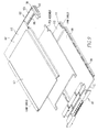
- the top and bottom card shields 7 and 8 are identical stampings of sheet metal eg. stainless steel. Over a substantial length of the shield, at one side are preferably periodically spaced, located upstanding tabs 9, and on the other side at same locations and periodicity appropriate recesses 10. In addition, at the front side 13 of a shield are located two fixation tabs 11, while at the rear side of each shield are extension portions 12 which are perpendicularly bent to be flush with in front of the metal shield of the connector plug opening of I/O connector 1. Such a perpendicular bend results in an improved aesthetics and also prevents an opening between I/O connector and shield and prevents what is known as a "smile" effect of the card while allowing for proper axial positioning of the PCB assembly.
- a perpendicular bend results in an improved aesthetics and also prevents an opening between I/O connector and shield and prevents what is known as a "smile" effect of the card while allowing for proper axial positioning of the PCB assembly.
- the I/O connector is shown in Figs. 5a and 5b in which it is shown that plastic is removed at ends of the top and bottom plastic walls 20 to allow the entry from the rear (PCB side) of two metal springs with legs 21 and 22 having inwardly projecting latches 23 and 24 and ends 25 and 26.
- the latches 23 and 24 contact the metal shield plug connector 18 of assembled I/O plug connector while the ends 25 and 26 are pressed on metal upper and lower shields 7 and 8 to complete the total ground connection of system.
- These two metal spring members are connected to the ground track on the PCB at two connector ends by rivets, as in initial design.
- FIGs. 6a - 6b another embodiment is shown in which one metal piece is inserted over for the top and bottom plastic walls of receptacle I/O connector.
- the advantage in this arrangement being not only, is one part needed, but that the metal shield extends over the total length of the connector while ensuring there is no potential drop between the two ground locations situated at connector ends.
- the inward projecting latches 23 and 24 face the central plastic insert 13 to finally connect with mating plug I/O shield 18.
- the outward latches 27 of the other side of the I/O connector contact the upper and lower shields 7 and 8, while the edges 25 and 26 are located also against the edges of the card shields.
- FIGs. 7-8 a further development of the I/O receptacle shield in combination with the substitute for ground contact 7 in initial design, is shown.
- the upper and shield portions are shown as two separate halfs, each with symmetrical segments of latch retaining openings 12 facing towards each other.
- This design alternative is not only present a metal plate with latch retaining openings, but also present at the rear end 28 of the receptacle I/O, besides the area needed for SMT legs of terminals, a metal wall over the remaining width of the card.
- This feature is more clearly evident in Fig. 4 showing the rear from the PCB side view of the receptacle I/O.
- This rear end 28 (Fig. 8) in this design when locked above a similar wall extending from lower shield portion, then affords a means for EMI/ESD shielding between the PCB electronics circuit I/O connector on this side of the card assembly.
- the PCB assembly includes the metallized receptacle I/O connector 101 at one end and the 68 pos MTB receptacle connector 102 at the other end of the board.
- This MTB connector 102 has the two coding keys 103 and 104 integrated to sides of the plastic housing, simultaneously an upstanding ridge 105 on the top and bottom of this housing.
- the I/O receptacle is described in detail hereafter.
- the top and bottom card shields 107 and 108 are sheet metal e.g. stainless steel. Over a substantial length of the shield, at one side are periodically located upstanding tabs 109, and on the other side at same locations and periodicity are appropriate recesses 110. In addition, at the front side 113 of a shield is located a fixation tab 111, and at the rear side of the shield are extension portions 112 which are perpendicularly bent to be flush with in front of the metal shield of the connector plug opening of I/O connector 101 in the final card assembly condition. Such a perpendicular bend results in an improved aesthetics of the card while allowing for proper longitudinal axial positioning of the PCB assembly.
- the tabs 109 cooperate with recess 110 along side and fixation tabs 111 cooperate with oppositely positioned recess 144 on the opposite side of the top shield through slot 100, to obtain a final card assembly.
- FIG. 9 -10 and 14 a further development of the I/O receptacle shield in combination with the substitute for ground contact 107 in initial design, is shown.
- the upper and shield portions are shown as two separate halfves each with symmetrical segments of latch retaining openings 112 facing towards each other.
- This design is not only present at a metal plate with latch retaining openings, but also present at the rear end 128 of the receptacle I/O, besides the area needed for SMT legs of terminals, a metal wall over the remaining width of the card.
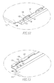
- Fig. 11 and 12 shows modified forms of securing tabs wherein the tabs 109 comprise an upstanding arcuate section 130 having opposed rigid sides 131 and chamfers 132 from which a spring latch 133 extends downwardly and outwardly.
- the recesses 110 are formed in a ledge 134.
- the ends of the recesses 110 have edges 135 and 136 which are angled inwardly to points 138.
- the tab 133 engages the underside of ledges 134 in the recesses 110.
- the two card shields of this embodiment are preferably made from 0.2mm stainless steel and have a number of mechanical snap fit fasteners. After assembling the two shields to each other, these fasteners make the card surprisingly and unexpectantly rigid and stiff against bending and torsion. These fasteners also effect good electrical connection for grounding between the two card shields due to multiple contact points, and also because no intermediate load bearing surfaces are utilized the card is optimally shielded for EMI.
- These fasteners comprise a number of tabs 109 which engage recesses 110. It will be seen from the drawings (in parts at Figs. 15 and 16) that each of the tabs 109 and latch 133 are angled inwardly from the perpendicular plane, for example, by angle of (Fig.
- Each tab 109 comprises a spring section 132 integrated with a latch 133, which hooks in a latch 134 underneath the area of each recess 110.
- This latch 133 holds the two card shields from opening after assembly. During mating, the tab 109 will be subjected to elastic bending and torsion forces from the tip of latch 133 up both rigid sides.
- Each tab 109 includes also two rigid sides 131 which engage with some play in both ends of the recess 110.
- the total number of rigid sides 131 and recess ends give the mechanical connection between the two card shields a high shear strength, which results in a high stiffness against bending and torsion.
- the two card shields are identical and are hermaphodite, that is, each shield contains both male and female fastening elements.
- the chamfers 132 will first touch the leading edges 135 and 136 so that they will guide the tab 109 to the end position beyond points 138 and guarantee that the latch 133 will hook underneath edge 134.
- the points 138 function as latches to hold the tab in position in the recess and provide an audible "snap" that indicates proper latching.
- the relative dimensions of the chamfers 132 and ledges 135 and 136 are designed to absorb manufacturing (stamping) tolerances.
- the latch mechanism is designed in a way that there is an initial play between the latch and the ledge 134 in vertical direction, which is taken away by a second spring function of ends 137 of the ledge. As these ends have a bending angle less than 90°, these make first contact when assembling the two card shields and then these have to be pressed together a little before the latch 133 will be mated. After that the latch mechanism has no further play.
- the overall cumulative lengths of the spring like tabs will be at least 10% of the length of the shield and more preferably will be 50% of the length of the shield.
- Fig. 9 it will also be seen that there is a slot 106 at each end of the connector 102, which allows the tab 111 to pass through the connector to engage a recess 144 in the opposing card shield.
- a completely metal to metal contact so that it is not necessary to engage the plastic in the connector 102. More particularly, if only two card shields 107 and 108 are engaged without using the connector 101 and 102 the resulting card case is rigid.
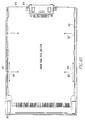
- FIGs. 18 - 21 an embodiment is shown in which no I/O receptacle is employed. Otherwise this embodiment is generally the same as that described in Figs. 9 - 17. That is, it has identical tabs 245 which engage identical recesses 254, and it also has a space 240 for an MTB connector (not shown).
- the joining tabs and recesses of the rear are disposed to the side and there is centrally adjoining panels 241 and 242.
- FIGs. 22 - 24 another embodiment is shown which is similar to the foregoing embodiment except that it makes use of a single 15 position I/O connector 343.
- the tabs 309 and recesses 310 are the same as was described above.
- the connecting tabs and recesses 345 and 354 respectively are positioned outwardly adjacent the I/O connector on the front end of the card while tabs 311 and recess 344 cooperate with each other on the MTV connector side.
- FIG. 25 - 27 another embodiment is shown which makes use of two I/O connectors 446 and 447. Otherwise this embodiment is essentially the same as the ones described above. It will be noted that at the rear end of this card the tab and recess 448 are positioned between the I / O connectors and the rear side of the card.
- Figs. 28 - 29 it will be seen that the full metal corners of the embodiments described above are comprised of a folded metal wall shown generally at 549.
- Figs. 30 - 31 it we be noted that this curved corner may be produced from a blank having a medial protrusion 450 and lateral protrusions 451 and 452 which may be folded upwardly and inwardly in segments to produce the desired rounded effect.
- EMI EST shielding or similar full metal shielding without use of plastic or open air. This feature is also aesthetically advantageous since it has no sharp edges.
- means are provided to appropriately align the two end connectors (I/O and the MTB connector) with respect to the PCB before their fixation by a solder reflow process.
- this alignment should be achieved without the need of tight connector peg-to-board hole clearances. Removing this requirement for both or one (e.g. MTB side) PCMCIA case would suffice.
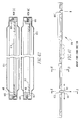
- the embodiment includes the incorporation of a plastic bar which is attached to one side edge of the metal card shield as shown in Fig. 33. Since the frame-bar's attachment along the longitudinal direction in the card shield is a key subject, forthcoming discussion and diagrams are related to the combination. The same frame-bar is utilized in the top and bottom shields.
- Fig. 34 shows two different views (in addition to a 360 rotation of second view with respect to the first) of one such frame-bar 601 having several upstanding lobes 602 and two longitudinally separated upstanding pegs 603 towards its middle portion, while several tapered recessed areas 604 are distributed over its length.
- Each lobe has one vertical face 605 and a tapered face 607; this vertical face of all lobes form one integral vertical face as at 605 extending over the length of the frame-bar 601.
- This protrusion is along a semicircular periphery 608 and 608', which both protrude from vertical face 605 in a space adjacent to the PCB edge.
- This protrusion towards the PCB is slightly different for these two pegs 603 and 603' due to a slight difference in their sizes and it faces the metal card shield edge 610.
- the user can locate such an assembly on a previously prepared combination of frame 201 with metal card 613.
- Fig. 49 (without an I/O connector), the pegs 603 and 603' allow for the fixation of this assembly, as discussed previously. Looking from the I/O to the MTB connector side, and assuming that the PCB and connector tails are transparent, results in Fig. 38. Different perspective views can be derived from Fig. 39.
- Fig. 40 shows another aspect of this design useful in "inverse" application of a card assembly. Due to the coding keys, such a card may be inserted only in one direction into the peripheral equipment. By inverted application (misuse), large longitudinal forces may be transmitted by the MTB connector to through the solder legs to the PCB 616. If the user continues to insert push the card from the I/O side, there may be a mechanical rupture to the solder joints on PCB, destroying the card. As evident in Fig. 40, the rear end 624 of the MTB connector in this design butts against the front of the frame 601. Since the latter is fixed in the case, such forces may be easily withstood by the edges of the PCB before force is transmitted to the solder connection.
- the current specification for PCMCIA cards is 60 Newton.
- the peg lobes 602 shown in this figure as a cross-section over the total width of one lobe of the frame-bar 601 enter from opposite shield sides and locate in appropriate recesses in the shield edges 610, the relative longitudinal movements between the two shields are immobilized. Again, this immobilization mechanism is distributed on several locations, on both sides of the PCMCIA card (in the length direction). Many other designs are prone to failure in this mode of loading. This, therefore, is a significant advantage of this design.
- the integration of the frame-bar gives a further enhancement of assembly robustness in addition to an extra safeguard (PCB alignment/positioning and fixation) to the electronic circuitry contained within the case.
Landscapes
- Engineering & Computer Science (AREA)
- Microelectronics & Electronic Packaging (AREA)
- Computer Hardware Design (AREA)
- Physics & Mathematics (AREA)
- General Physics & Mathematics (AREA)
- Theoretical Computer Science (AREA)
- Details Of Connecting Devices For Male And Female Coupling (AREA)
- Credit Cards Or The Like (AREA)
- Shielding Devices Or Components To Electric Or Magnetic Fields (AREA)
Claims (34)
- Elektronische Karte mit einer gedruckten Leiterplattenanordnung zwischen Kartenabschirmungen mit Kanten, wobei auf den Kanten einer Abschirmung Zungen vorgesehen sind, die in Öffnungen auf der Kante der anderen Abschirmung eingreifen und wobei jede dieser Zungen ein Glied mit einem schrägen Vorsprung aufweist, welches in die andere Abschirmung eingreift, und ein Rahmen zwischen den Abschirmungen angeordnet ist, wobei die gedruckte Leiterplattenanordnung von Rahmenstegen getragen ist und wobei die Abschirmungen hermaphroditisch sind.
- Karte nach Anspruch 1, wobei jede Abschirmung eine Leiste in ihrem Rahmen aufweist und die Öffnung in dieser Leiste angeordnet ist und der Vorsprung auf der Zunge in diese Leiste eingreift.
- Karte nach Anspruch 1, wobei die Öffnung gewinkelte Enden aufweist, in die die gebogenen Glieder der Zungen eingreifen.
- Karte nach Anspruch 1, wobei die Zungen elastisch sind.
- Karte nach Anspruch 4, wobei jede der Zungen über ihre gesamte Länge elastisch ist.
- Karte nach Anspruch 5, wobei die Zungen als Federn fungieren.
- Karte nach Anspruch 6, wobei die Zungen über ihre gesamte Länge als Federn fungieren.
- Karte nach Anspruch 7, wobei die Karte eine bestimmte Länge aufweist und die Zungen eine kumulative Länge aufweisen und wobei die kumulative Länge der Zungen mindestens 10% der Länge der Karte beträgt.
- Karte nach Anspruch 8, wobei die Karte eine Länge aufweist und die Zungen eine kumulative Länge aufweisen, wobei die kumulative Länge der Zungen mindestens 50% der Länge der Karte beträgt.
- Karte nach Anspruch 1, die Biegekräfte aushält, deren erforderliche Werte in Tests spezifiziert sind.
- Karte nach Anspruch 1, die Torsionskräften widersteht, ohne Verwendung von Endverbindern.
- Karte nach Anspruch 1 mit mindestens einer im Wesentlichen abgeflachten Ecke.
- Karte nach Anspruch 1, bei der die gedruckte Leiterplatte vollständig von einem Metallmaterial umhüllt ist.
- Karte nach Anspruch 13, mit mindestens einer im Wesentlichen flachen Ecke.
- Karte nach Anspruch 14, mit mindestens einer Ecke, die eine diagonal verlaufende Metallwand ist.
- Karte nach Anspruch 15, wobei die diagonal verlaufende Metallwand durch Falten einer Projektion einer Abschirmung nach hinten auf die Abschirmung zu geformt ist.
- Karte nach Anspruch 1, wobei die Deckel- und Bodenabschirmungen identisch sind.
- Karte nach Anspruch 1, wobei die Kartenabschirmungen Ecken aufweisen, von denen wenigstens eine abgeflacht ist.
- Karte nach Anspruch 18, wobei die gedruckte Leiterplatte vollständig von Metall umhüllt ist.
- Karte nach Anspruch 1, wobei die Glieder schräge, vorspringende Bögen aufweisen.
- Karte nach Anspruch 1, die sowohl Torsions- als auch Scherkräften widersteht.
- Karte nach Anspruch 21, die sowohl Torsions- als auch Scherkräften bei Verwendung von Endverbindern widersteht.
- Karte nach mindestens einem der vorstehenden Ansprüche, wobei die Karte eine Speicherkarte ist und die Abschirmungen Ecken aufweisen und mindestens eine dieser Ecken abgeflacht ist.
- Karte nach Anspruch 1, wobei ein hörbares Einschnappgeräusch aus dem Einrasten der Abschirmungen resultiert.
- Karte nach Anspruch 1, wobei die Öffnungen gegenüberliegende Kanten aufweisen, die auf Punkte zu nach außen abgewinkelt sind.
- Karte nach Anspruch 25, wobei die Zunge in die Öffnung eingreift und die Zunge in ihre Position gezwungen wird.
- Karte nach Anspruch 1, mit einem Eingangs-/Ausgangsverbinder, der ohne separaten Erdungskontakt geerdet ist.
- Karte nach Anspruch 1, wobei der Eingangs-/Ausgangsverbinder eine Länge aufweist und der Verbinder über seine Länge abgeschirmt ist.
- Karte nach Anspruch 1, wobei mindestens eine Öffnung einen Schlitz und eine Nockenstruktur aufweist, um die Zunge seitlich in den Schlitz zu bewegen, wenn die Zunge sich auf die Öffnung zu bewegt.
- Karte nach Anspruch 29, wobei die Nockenstrukturen ein paar divergierender Wände aufweist.
- Karte nach Anspruch 30, wobei jede divergierende Wand den Schlitz an einer Stelle kreuzt, die von einem Ende des Schlitzes beabstandet ist.
- Karte nach Anspruch 1, wobei jede Öffnung einen Vorsprung aufweist zum Eingriff der Klinke einer jeden Zunge.
- Karte nach Anspruch 1, wobei die Kartenabschirmungen jeweils aufweisen: eine Kante, die die inneren und äußeren Perimeter der elektronischen Karte definieren, wobei die Kante einen inneren Bereich aufweist, der dem äußeren Umfang der elektronischen Karte gegenüberliegt, eine Klinkenstruktur zum Eingriff in eine entsprechende Klinkenstruktur auf der anderen Abschirmung und einen Rahmensteg, der sich entlang dem inneren Bereich der Kante der Abschirmung erstreckt, wobei der Rahmensteg einen ersten Aufbau zur Positionierung des Rahmenstegs bezüglich der zweiten einsteckbaren Abschirmung aufweist und einen zweiten Aufbau zur Positionierung der ersten steckbaren Abschirmung bezüglich der anderen Abschirmung.
- Karte nach Anspruch 33, wobei der innere Bereich der Abschirmung ferner eine Öffnung aufweist, der erste Aufbau einen Stift und einen Bereich des Rahmenstegs, der sich unter die Öffnung erstreckt und der zweite Aufbau vertikale Lappen aufweist.
Priority Applications (1)
| Application Number | Priority Date | Filing Date | Title |
|---|---|---|---|
| EP06014852A EP1717734B1 (de) | 1996-11-08 | 1997-08-13 | Elektonische Kartenanordnung |
Applications Claiming Priority (5)
| Application Number | Priority Date | Filing Date | Title |
|---|---|---|---|
| US08/748,503 US6058018A (en) | 1996-04-05 | 1996-11-08 | Electronic card |
| US748503 | 1996-11-08 | ||
| US4739897P | 1997-05-22 | 1997-05-22 | |
| US47398P | 1997-05-22 | ||
| PCT/US1997/014369 WO1998020451A1 (en) | 1996-11-08 | 1997-08-13 | Electronic card |
Related Child Applications (1)
| Application Number | Title | Priority Date | Filing Date |
|---|---|---|---|
| EP06014852A Division EP1717734B1 (de) | 1996-11-08 | 1997-08-13 | Elektonische Kartenanordnung |
Publications (3)
| Publication Number | Publication Date |
|---|---|
| EP0939937A1 EP0939937A1 (de) | 1999-09-08 |
| EP0939937A4 EP0939937A4 (de) | 2000-03-15 |
| EP0939937B1 true EP0939937B1 (de) | 2007-04-04 |
Family
ID=26724979
Family Applications (1)
| Application Number | Title | Priority Date | Filing Date |
|---|---|---|---|
| EP97938323A Expired - Lifetime EP0939937B1 (de) | 1996-11-08 | 1997-08-13 | Elektronische Karte |
Country Status (7)
| Country | Link |
|---|---|
| US (2) | US6533177B1 (de) |
| EP (1) | EP0939937B1 (de) |
| JP (2) | JP4031048B2 (de) |
| KR (1) | KR100512232B1 (de) |
| CN (1) | CN1142709C (de) |
| DE (1) | DE69737559T2 (de) |
| WO (1) | WO1998020451A1 (de) |
Cited By (1)
| Publication number | Priority date | Publication date | Assignee | Title |
|---|---|---|---|---|
| TWI682702B (zh) * | 2018-09-17 | 2020-01-11 | 廣達電腦股份有限公司 | 用於計算裝置的機箱 |
Families Citing this family (15)
| Publication number | Priority date | Publication date | Assignee | Title |
|---|---|---|---|---|
| US6151219A (en) * | 1999-02-01 | 2000-11-21 | Itt Manufacturing Enterprises, Inc. | Electronic card with sheet metal and overmolded plastic frame parts |
| FR2812167B1 (fr) * | 2000-07-19 | 2004-09-10 | Fci Besancon Sa | Boitier muni d'une extension d'antenne pour carte electronique et procede d'assemblage du boitier |
| US6556170B2 (en) | 2001-04-02 | 2003-04-29 | Fci Americas Technology, Inc. | Retractable and rotatable antenna for an electronic card |
| DE20208803U1 (de) * | 2002-06-06 | 2002-09-12 | Gu, Yin-Tsair, Hsin Tien, Taipeh | Netzkarte eines Computers mit verbesserter Erdung |
| FI116325B (fi) * | 2003-12-03 | 2005-10-31 | Nokia Corp | Muistikortin kytkentäelin |
| TWM276353U (en) * | 2005-02-03 | 2005-09-21 | Egbn Electronics Ltd | Card edge connector |
| WO2007046789A1 (en) * | 2005-10-17 | 2007-04-26 | Duel Systems | Electronic packages for peripheral devices |
| US8099794B2 (en) | 2005-12-19 | 2012-01-24 | Rusl, Llc | Body conforming textile holder for electronic device |
| US7489515B2 (en) * | 2006-10-31 | 2009-02-10 | Broadtek Technology Co., Ltd. | Expansion card |
| ITUD20080252A1 (it) * | 2008-12-04 | 2010-06-05 | Sata Hts Hi Tech Services S P A | "processo di interfacciamento con dispositivo di interfacciamento portatile per smart-card e relativo dispositivo di interfacciamento portatile per smart-card" |
| JP2010165311A (ja) | 2009-01-19 | 2010-07-29 | Jst Mfg Co Ltd | Icカード |
| EP2835876A1 (de) * | 2013-08-05 | 2015-02-11 | Continental Automotive GmbH | Modulgehäuse für elektronische Baugruppe |
| US9468116B2 (en) * | 2014-04-11 | 2016-10-11 | Seagate Technology Llc | Secure enclosure |
| DE102016220022B4 (de) | 2016-10-13 | 2021-12-09 | Vitesco Technologies GmbH | Kombination eines Steckers mit einem Deckel |
| KR102606483B1 (ko) * | 2016-10-17 | 2023-11-30 | 삼성전자주식회사 | 인쇄회로기판 및 이를 포함하는 솔리드 스테이트 드라이브 |
Family Cites Families (37)
| Publication number | Priority date | Publication date | Assignee | Title |
|---|---|---|---|---|
| US4872878A (en) * | 1987-03-17 | 1989-10-10 | Dennis T. Grendahl | Optical brigthener in an intraocular lens |
| DE8714913U1 (de) | 1987-11-09 | 1988-01-07 | Du Pont de Nemours (Nederland) B.V., Dordrecht | Abdeckhaube für eine Kontaktleiste |
| JPH0463284A (ja) | 1990-07-02 | 1992-02-28 | Canon Inc | マイクロ波プラズマcvd装置 |
| US5144533A (en) * | 1991-06-27 | 1992-09-01 | Motorola, Inc. | Self-locking housing assembly |
| US5207586A (en) * | 1991-10-24 | 1993-05-04 | Intel Corporation | Integral connector system for credit card size I/O card external connector |
| CA2057518C (en) * | 1991-12-09 | 1996-11-19 | Albert John Kerklaan | Jacketted circuit card |
| US5330360A (en) * | 1992-08-21 | 1994-07-19 | The Whitaker Corporation | Memory card and connector therefor |
| US5377060A (en) * | 1992-09-02 | 1994-12-27 | Antek Peripherals, Inc. | Ultra slim data storage module utilizing plural flexible disks |
| US5339222A (en) * | 1993-04-06 | 1994-08-16 | The Whitaker Corporation | Shielded printed circuit card holder |
| US5476387A (en) * | 1993-06-07 | 1995-12-19 | Methode Electronics Inc. | Memory card frame and cover kit |
| US5397857A (en) * | 1993-07-15 | 1995-03-14 | Dual Systems | PCMCIA standard memory card frame |
| US5687064A (en) * | 1993-08-31 | 1997-11-11 | Wireless Access, Inc. | Rigidized outer support structure for an integrated circuit card |
| JP2581343Y2 (ja) * | 1993-09-10 | 1998-09-21 | 本多通信工業株式会社 | Icカード |
| US5409385A (en) * | 1993-10-07 | 1995-04-25 | Genrife Company Limited | I/O card and connection mechanism thereof |
| US5477426A (en) * | 1993-12-15 | 1995-12-19 | Itt Corporation | IC card with board positioning means |
| DE4341104C1 (de) * | 1993-12-02 | 1995-01-12 | Harting Elektronik Gmbh | Abgeschirmte Leiterplattensteckverbindung |
| US5563770A (en) * | 1994-02-25 | 1996-10-08 | Itt Corporation | IC card with board positioning means |
| DE4406644C2 (de) * | 1994-03-01 | 1997-12-18 | Itt Cannon Gmbh | Steckkarte für elektronische Datenverarbeitungsgeräte und Verfahren zu dessen Herstellung und Montage |
| US5736646A (en) * | 1994-03-09 | 1998-04-07 | International Business Machines Corporation | Circuit board assembly torsion tester and method |
| US5567884A (en) * | 1994-03-09 | 1996-10-22 | International Business Machines Corporation | Circuit board assembly torsion tester and method |
| US5478259A (en) * | 1994-03-28 | 1995-12-26 | Burndy Corporation | Card edge connector with combined shielding and voltage drain protection |
| US5536905A (en) * | 1994-04-04 | 1996-07-16 | Motorola, Inc. | Self secured housing for electronics |
| US5497297A (en) * | 1994-06-28 | 1996-03-05 | Intel Corporation | Frame and cover structure for integrated circuit cards |
| US5502892A (en) * | 1994-07-01 | 1996-04-02 | Maxconn Incorporated | Method of forming a welded encasement for a computer card |
| US5463531A (en) * | 1994-07-05 | 1995-10-31 | Motorola, Inc. | PCMCIA electronics housing |
| US5548483A (en) * | 1995-01-24 | 1996-08-20 | Elco Corporation | Frameless IC card and housing therefor |
| US5574628A (en) * | 1995-05-17 | 1996-11-12 | The Whitaker Corporation | Rigid PCMCIA frame kit |
| JPH09164791A (ja) * | 1995-12-19 | 1997-06-24 | Mitsubishi Electric Corp | Icカード及びその製造方法 |
| US6058018A (en) * | 1996-04-05 | 2000-05-02 | Berg Technology, Inc. | Electronic card |
| US6160711A (en) * | 1996-04-05 | 2000-12-12 | Berg Technology, Inc. | Electronic card |
| US5754404A (en) * | 1996-05-14 | 1998-05-19 | Itt Cannon Gmbh | IC card rear board-connector support |
| US5689405A (en) * | 1996-09-25 | 1997-11-18 | Itt Corporation | IC card rear board support |
| US5833473A (en) * | 1997-03-12 | 1998-11-10 | Itt Manufacturing Enterprises, Inc. | Cardbus Bridge |
| US5984731A (en) * | 1997-11-17 | 1999-11-16 | Xircom, Inc. | Removable I/O device with integrated receptacles for receiving standard plugs |
| US6116962A (en) * | 1997-11-17 | 2000-09-12 | Xircom Inc | Type III PCMCIA card with integrated receptacles for receiving standard communications plugs |
| JP2004180903A (ja) * | 2002-12-03 | 2004-07-02 | Kinshi:Kk | クッション体 |
| JP4492807B2 (ja) * | 2005-10-11 | 2010-06-30 | 俊郎 高城 | 流動性をもつ粒状材料 |
-
1997
- 1997-08-13 CN CNB971995575A patent/CN1142709C/zh not_active Expired - Fee Related
- 1997-08-13 EP EP97938323A patent/EP0939937B1/de not_active Expired - Lifetime
- 1997-08-13 DE DE69737559T patent/DE69737559T2/de not_active Expired - Lifetime
- 1997-08-13 US US09/297,776 patent/US6533177B1/en not_active Expired - Fee Related
- 1997-08-13 WO PCT/US1997/014369 patent/WO1998020451A1/en not_active Ceased
- 1997-08-13 KR KR10-1999-7004106A patent/KR100512232B1/ko not_active Expired - Fee Related
- 1997-08-13 JP JP52135898A patent/JP4031048B2/ja not_active Expired - Fee Related
-
2001
- 2001-07-27 US US09/916,491 patent/US6905073B2/en not_active Expired - Fee Related
-
2007
- 2007-01-18 JP JP2007008984A patent/JP2007193809A/ja not_active Ceased
Cited By (2)
| Publication number | Priority date | Publication date | Assignee | Title |
|---|---|---|---|---|
| TWI682702B (zh) * | 2018-09-17 | 2020-01-11 | 廣達電腦股份有限公司 | 用於計算裝置的機箱 |
| US10869403B2 (en) | 2018-09-17 | 2020-12-15 | Quanta Computer Inc. | Elastomer design for computing device chassis |
Also Published As
| Publication number | Publication date |
|---|---|
| KR20000053167A (en) | 2000-08-25 |
| CN1236460A (zh) | 1999-11-24 |
| US6905073B2 (en) | 2005-06-14 |
| DE69737559D1 (de) | 2007-05-16 |
| JP4031048B2 (ja) | 2008-01-09 |
| US20020053599A1 (en) | 2002-05-09 |
| EP0939937A1 (de) | 1999-09-08 |
| US6533177B1 (en) | 2003-03-18 |
| EP0939937A4 (de) | 2000-03-15 |
| JP2002513482A (ja) | 2002-05-08 |
| CN1142709C (zh) | 2004-03-17 |
| DE69737559T2 (de) | 2007-12-20 |
| JP2007193809A (ja) | 2007-08-02 |
| KR100512232B1 (ko) | 2005-09-05 |
| WO1998020451A1 (en) | 1998-05-14 |
Similar Documents
| Publication | Publication Date | Title |
|---|---|---|
| US6058018A (en) | Electronic card | |
| EP0939937B1 (de) | Elektronische Karte | |
| US5780365A (en) | PC card frame kit and PC card | |
| JP4334662B2 (ja) | Icカード用フレームキットおよびicカード | |
| US5912806A (en) | IC card of simple structure | |
| US6324076B1 (en) | Electronic card with shield cover having tabs where each tab engages with recess of corresponding shield cover | |
| JP3370857B2 (ja) | コネクタ | |
| JPH09164791A (ja) | Icカード及びその製造方法 | |
| US6160711A (en) | Electronic card | |
| EP1717734B1 (de) | Elektonische Kartenanordnung | |
| KR20030019594A (ko) | 전자 카드용 안테나 연장부를 구비한 팩 및 팩의 조립 방법 | |
| EP1013156B1 (de) | Elektronische karte | |
| KR100479397B1 (ko) | 대응하는차폐커버의리세스와맞물리는탭들을갖는차폐커버를구비한전자카드 | |
| JPH07220815A (ja) | 電気コネクタ | |
| JP2003036921A (ja) | シャッタ付きコネクタ | |
| JP2004265689A (ja) | カードアダプタ | |
| JP2009211266A (ja) | 電子カード | |
| WO1999014993A2 (en) | Electronic card with rf extension | |
| JPH08255661A (ja) | コネクタ | |
| JPH0528700Y2 (de) | ||
| CN100399348C (zh) | 硬卡 |
Legal Events
| Date | Code | Title | Description |
|---|---|---|---|
| PUAI | Public reference made under article 153(3) epc to a published international application that has entered the european phase |
Free format text: ORIGINAL CODE: 0009012 |
|
| 17P | Request for examination filed |
Effective date: 19990528 |
|
| AK | Designated contracting states |
Kind code of ref document: A1 Designated state(s): BE CH DE DK ES FI FR GB IE IT LI NL SE |
|
| A4 | Supplementary search report drawn up and despatched |
Effective date: 20000131 |
|
| AK | Designated contracting states |
Kind code of ref document: A4 Designated state(s): BE CH DE DK ES FI FR GB IE IT LI NL SE |
|
| RIC1 | Information provided on ipc code assigned before grant |
Free format text: 7H 05K 1/14 A, 7H 05K 5/02 B, 7G 06K 19/077 B |
|
| GRAP | Despatch of communication of intention to grant a patent |
Free format text: ORIGINAL CODE: EPIDOSNIGR1 |
|
| RTI1 | Title (correction) |
Free format text: ELECTRONIC CARD |
|
| GRAS | Grant fee paid |
Free format text: ORIGINAL CODE: EPIDOSNIGR3 |
|
| RAP1 | Party data changed (applicant data changed or rights of an application transferred) |
Owner name: FCI |
|
| GRAA | (expected) grant |
Free format text: ORIGINAL CODE: 0009210 |
|
| AK | Designated contracting states |
Kind code of ref document: B1 Designated state(s): BE CH DE DK ES FI FR GB IE IT LI NL SE |
|
| PG25 | Lapsed in a contracting state [announced via postgrant information from national office to epo] |
Ref country code: LI Free format text: LAPSE BECAUSE OF FAILURE TO SUBMIT A TRANSLATION OF THE DESCRIPTION OR TO PAY THE FEE WITHIN THE PRESCRIBED TIME-LIMIT Effective date: 20070404 Ref country code: FI Free format text: LAPSE BECAUSE OF FAILURE TO SUBMIT A TRANSLATION OF THE DESCRIPTION OR TO PAY THE FEE WITHIN THE PRESCRIBED TIME-LIMIT Effective date: 20070404 Ref country code: CH Free format text: LAPSE BECAUSE OF FAILURE TO SUBMIT A TRANSLATION OF THE DESCRIPTION OR TO PAY THE FEE WITHIN THE PRESCRIBED TIME-LIMIT Effective date: 20070404 |
|
| REG | Reference to a national code |
Ref country code: GB Ref legal event code: FG4D |
|
| REG | Reference to a national code |
Ref country code: CH Ref legal event code: EP |
|
| REF | Corresponds to: |
Ref document number: 69737559 Country of ref document: DE Date of ref document: 20070516 Kind code of ref document: P |
|
| REG | Reference to a national code |
Ref country code: IE Ref legal event code: FG4D |
|
| PG25 | Lapsed in a contracting state [announced via postgrant information from national office to epo] |
Ref country code: SE Free format text: LAPSE BECAUSE OF FAILURE TO SUBMIT A TRANSLATION OF THE DESCRIPTION OR TO PAY THE FEE WITHIN THE PRESCRIBED TIME-LIMIT Effective date: 20070704 |
|
| PG25 | Lapsed in a contracting state [announced via postgrant information from national office to epo] |
Ref country code: ES Free format text: LAPSE BECAUSE OF FAILURE TO SUBMIT A TRANSLATION OF THE DESCRIPTION OR TO PAY THE FEE WITHIN THE PRESCRIBED TIME-LIMIT Effective date: 20070715 |
|
| ET | Fr: translation filed | ||
| NLV1 | Nl: lapsed or annulled due to failure to fulfill the requirements of art. 29p and 29m of the patents act | ||
| REG | Reference to a national code |
Ref country code: CH Ref legal event code: PL |
|
| PG25 | Lapsed in a contracting state [announced via postgrant information from national office to epo] |
Ref country code: BE Free format text: LAPSE BECAUSE OF FAILURE TO SUBMIT A TRANSLATION OF THE DESCRIPTION OR TO PAY THE FEE WITHIN THE PRESCRIBED TIME-LIMIT Effective date: 20070404 |
|
| PGFP | Annual fee paid to national office [announced via postgrant information from national office to epo] |
Ref country code: GB Payment date: 20070705 Year of fee payment: 11 |
|
| PG25 | Lapsed in a contracting state [announced via postgrant information from national office to epo] |
Ref country code: NL Free format text: LAPSE BECAUSE OF FAILURE TO SUBMIT A TRANSLATION OF THE DESCRIPTION OR TO PAY THE FEE WITHIN THE PRESCRIBED TIME-LIMIT Effective date: 20070404 Ref country code: DK Free format text: LAPSE BECAUSE OF FAILURE TO SUBMIT A TRANSLATION OF THE DESCRIPTION OR TO PAY THE FEE WITHIN THE PRESCRIBED TIME-LIMIT Effective date: 20070404 |
|
| PLBE | No opposition filed within time limit |
Free format text: ORIGINAL CODE: 0009261 |
|
| STAA | Information on the status of an ep patent application or granted ep patent |
Free format text: STATUS: NO OPPOSITION FILED WITHIN TIME LIMIT |
|
| 26N | No opposition filed |
Effective date: 20080107 |
|
| PGFP | Annual fee paid to national office [announced via postgrant information from national office to epo] |
Ref country code: FR Payment date: 20070803 Year of fee payment: 11 |
|
| PG25 | Lapsed in a contracting state [announced via postgrant information from national office to epo] |
Ref country code: IE Free format text: LAPSE BECAUSE OF NON-PAYMENT OF DUE FEES Effective date: 20070813 |
|
| GBPC | Gb: european patent ceased through non-payment of renewal fee |
Effective date: 20080813 |
|
| REG | Reference to a national code |
Ref country code: FR Ref legal event code: ST Effective date: 20090430 |
|
| PG25 | Lapsed in a contracting state [announced via postgrant information from national office to epo] |
Ref country code: FR Free format text: LAPSE BECAUSE OF NON-PAYMENT OF DUE FEES Effective date: 20080901 |
|
| PG25 | Lapsed in a contracting state [announced via postgrant information from national office to epo] |
Ref country code: GB Free format text: LAPSE BECAUSE OF NON-PAYMENT OF DUE FEES Effective date: 20080813 |
|
| REG | Reference to a national code |
Ref country code: DE Ref legal event code: R082 Ref document number: 69737559 Country of ref document: DE Representative=s name: BARDEHLE PAGENBERG PARTNERSCHAFT MBB PATENTANW, DE Effective date: 20120419 Ref country code: DE Ref legal event code: R081 Ref document number: 69737559 Country of ref document: DE Owner name: FCI, FR Free format text: FORMER OWNER: FCI, VERSAILLES, FR Effective date: 20120419 |
|
| PGFP | Annual fee paid to national office [announced via postgrant information from national office to epo] |
Ref country code: IT Payment date: 20120820 Year of fee payment: 16 Ref country code: DE Payment date: 20120831 Year of fee payment: 16 |
|
| PG25 | Lapsed in a contracting state [announced via postgrant information from national office to epo] |
Ref country code: DE Free format text: LAPSE BECAUSE OF NON-PAYMENT OF DUE FEES Effective date: 20140301 |
|
| REG | Reference to a national code |
Ref country code: DE Ref legal event code: R119 Ref document number: 69737559 Country of ref document: DE Effective date: 20140301 |
|
| PG25 | Lapsed in a contracting state [announced via postgrant information from national office to epo] |
Ref country code: IT Free format text: LAPSE BECAUSE OF NON-PAYMENT OF DUE FEES Effective date: 20130813 |