EP0941021A1 - Procédé de fabrication de panneaux à circuit imprimé à connexion électrique entre les faces - Google Patents
Procédé de fabrication de panneaux à circuit imprimé à connexion électrique entre les faces Download PDFInfo
- Publication number
- EP0941021A1 EP0941021A1 EP98500066A EP98500066A EP0941021A1 EP 0941021 A1 EP0941021 A1 EP 0941021A1 EP 98500066 A EP98500066 A EP 98500066A EP 98500066 A EP98500066 A EP 98500066A EP 0941021 A1 EP0941021 A1 EP 0941021A1
- Authority
- EP
- European Patent Office
- Prior art keywords
- faces
- circuit
- electrical connection
- printed
- copper
- Prior art date
- Legal status (The legal status is an assumption and is not a legal conclusion. Google has not performed a legal analysis and makes no representation as to the accuracy of the status listed.)
- Withdrawn
Links
Images

Classifications
-
- H—ELECTRICITY
- H05—ELECTRIC TECHNIQUES NOT OTHERWISE PROVIDED FOR
- H05K—PRINTED CIRCUITS; CASINGS OR CONSTRUCTIONAL DETAILS OF ELECTRIC APPARATUS; MANUFACTURE OF ASSEMBLAGES OF ELECTRICAL COMPONENTS
- H05K3/00—Apparatus or processes for manufacturing printed circuits
- H05K3/40—Forming printed elements for providing electric connections to or between printed circuits
- H05K3/42—Plated through-holes or plated via connections
- H05K3/425—Plated through-holes or plated via connections characterised by the sequence of steps for plating the through-holes or via connections in relation to the conductive pattern
- H05K3/428—Plated through-holes or plated via connections characterised by the sequence of steps for plating the through-holes or via connections in relation to the conductive pattern initial plating of through-holes in substrates having a metal pattern
-
- H—ELECTRICITY
- H05—ELECTRIC TECHNIQUES NOT OTHERWISE PROVIDED FOR
- H05K—PRINTED CIRCUITS; CASINGS OR CONSTRUCTIONAL DETAILS OF ELECTRIC APPARATUS; MANUFACTURE OF ASSEMBLAGES OF ELECTRICAL COMPONENTS
- H05K3/00—Apparatus or processes for manufacturing printed circuits
- H05K3/30—Assembling printed circuits with electric components, e.g. with resistors
- H05K3/32—Assembling printed circuits with electric components, e.g. with resistors electrically connecting electric components or wires to printed circuits
- H05K3/34—Assembling printed circuits with electric components, e.g. with resistors electrically connecting electric components or wires to printed circuits by soldering
- H05K3/3465—Application of solder
- H05K3/3468—Application of molten solder, e.g. dip soldering
-
- H—ELECTRICITY
- H05—ELECTRIC TECHNIQUES NOT OTHERWISE PROVIDED FOR
- H05K—PRINTED CIRCUITS; CASINGS OR CONSTRUCTIONAL DETAILS OF ELECTRIC APPARATUS; MANUFACTURE OF ASSEMBLAGES OF ELECTRICAL COMPONENTS
- H05K2201/00—Indexing scheme relating to printed circuits covered by H05K1/00
- H05K2201/09—Shape and layout
- H05K2201/09209—Shape and layout details of conductors
- H05K2201/095—Conductive through-holes or vias
- H05K2201/09572—Solder filled plated through-hole in the final product
-
- H—ELECTRICITY
- H05—ELECTRIC TECHNIQUES NOT OTHERWISE PROVIDED FOR
- H05K—PRINTED CIRCUITS; CASINGS OR CONSTRUCTIONAL DETAILS OF ELECTRIC APPARATUS; MANUFACTURE OF ASSEMBLAGES OF ELECTRICAL COMPONENTS
- H05K2203/00—Indexing scheme relating to apparatus or processes for manufacturing printed circuits covered by H05K3/00
- H05K2203/04—Soldering or other types of metallurgic bonding
- H05K2203/044—Solder dip coating, i.e. coating printed conductors, e.g. pads by dipping in molten solder or by wave soldering
-
- H—ELECTRICITY
- H05—ELECTRIC TECHNIQUES NOT OTHERWISE PROVIDED FOR
- H05K—PRINTED CIRCUITS; CASINGS OR CONSTRUCTIONAL DETAILS OF ELECTRIC APPARATUS; MANUFACTURE OF ASSEMBLAGES OF ELECTRICAL COMPONENTS
- H05K3/00—Apparatus or processes for manufacturing printed circuits
- H05K3/30—Assembling printed circuits with electric components, e.g. with resistors
- H05K3/32—Assembling printed circuits with electric components, e.g. with resistors electrically connecting electric components or wires to printed circuits
- H05K3/34—Assembling printed circuits with electric components, e.g. with resistors electrically connecting electric components or wires to printed circuits by soldering
- H05K3/3452—Solder masks
Definitions
- the present invention refers to a new manufacturing process for printed-circuit boards, especially boards with electrical connections between faces, that supposes a notable simplification and a subsequent reduction in cost compared to conventional processes.
- the process is ideally suited for the type of printed-circuit boards used in the automobile industry and for electronic consumer goods such as video, hi-fi, television and telephony.
- the base materials used to obtain boards are fibreglass- and epoxy resin-based "FR-4" and "CEM-1", which is a material composed of Fiberglas, paper and epoxy resin.
- This type of board would first be metallized, then punched, metallized again and finally etched, leading to the elimination of the two copper layers in order to define the tracks.
- the process proposed by the invention resolves the aforementioned repercussions in a highly satisfactory way, considering that it renders bore holes useful for inserting components, leading to the reduction in size of the printed circuit in addition to a substantial improvement in the electrical characteristics of the printed circuit compared to the classic surfacing of the holes with "silver ink”.
- Metallization is also performed on laminates that cost less than the FR-4, avoiding the typical problems that traditional copper metallization has on these laminates.
- the process proposed by the invention enables bore holes to be used by chemically making a metallic deposit. This is to say, without electrolyte processes on one or more of the holes of the printed circuit, depending on its needs.
- This process can be applied to the majority of base materials available on the market, and, in particular, to the following types: CEM-3, CEM-1, FR-2 and FR-1.
- the manufacturing process begins with the preparation of the base material by means of wet-process polishing, leaving the copper in perfect condition for a second phase, silk-screening, in which the copper pattern of the circuit is impressed and the excess copper is eliminated by means of chemical etching.
- impression is performed with inks resistant to the chemical processes of metallization that will connect the two faces of the circuit, in addition to its punching.
- soldering mask is applied, along with identifying inks and other conductive inks.
- a soldering jet then ensures that the metallized bore holes are completely filled with tin/lead.
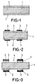
- the unit is punched, obtaining the bore holes (5) that are, in their number and positioning, suitable for the electrical connection between the two faces of the board as well as for the insertion of electronic components of the circuit.
- the unit again undergoes an impression with inks (6) resistant to the chemical processes of metallization in order to leave the areas (7) meant to connect the two faces of the circuit through the bore holes (5) clear.
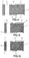
- the chemical metallization phase is then carried out, and, as it has been stated previously, it is performed with a nickel-phosphorous alloy (8), as seen in Figure 7.
- This chemical metallization (8) affects only those bore holes (5) where the connection between the two faces of the board is going to be carried out, while the normal holes (9) will not be affected by this metallizing.
- identifying inks and other conductive inks (10) are applied in order to improve adhesion so that the soldering mask represented in Figure 8 enables, after the soldering jet phase (shown in Figure 9), the metallized bore holes (5) to be completely filled with a tin/lead mass (11), while in the normal holes (9) the soldering mass (12) can be applied to only one of their openings, as is shown in Figure 9.
Landscapes
- Engineering & Computer Science (AREA)
- Manufacturing & Machinery (AREA)
- Microelectronics & Electronic Packaging (AREA)
- Printing Elements For Providing Electric Connections Between Printed Circuits (AREA)
Priority Applications (1)
| Application Number | Priority Date | Filing Date | Title |
|---|---|---|---|
| EP98500066A EP0941021A1 (fr) | 1998-03-06 | 1998-03-06 | Procédé de fabrication de panneaux à circuit imprimé à connexion électrique entre les faces |
Applications Claiming Priority (1)
| Application Number | Priority Date | Filing Date | Title |
|---|---|---|---|
| EP98500066A EP0941021A1 (fr) | 1998-03-06 | 1998-03-06 | Procédé de fabrication de panneaux à circuit imprimé à connexion électrique entre les faces |
Publications (1)
| Publication Number | Publication Date |
|---|---|
| EP0941021A1 true EP0941021A1 (fr) | 1999-09-08 |
Family
ID=8235808
Family Applications (1)
| Application Number | Title | Priority Date | Filing Date |
|---|---|---|---|
| EP98500066A Withdrawn EP0941021A1 (fr) | 1998-03-06 | 1998-03-06 | Procédé de fabrication de panneaux à circuit imprimé à connexion électrique entre les faces |
Country Status (1)
| Country | Link |
|---|---|
| EP (1) | EP0941021A1 (fr) |
Cited By (1)
| Publication number | Priority date | Publication date | Assignee | Title |
|---|---|---|---|---|
| CN109769344A (zh) * | 2017-11-10 | 2019-05-17 | 鹏鼎控股(深圳)股份有限公司 | 电路板及该电路板的制造方法 |
Citations (5)
| Publication number | Priority date | Publication date | Assignee | Title |
|---|---|---|---|---|
| GB1223939A (en) * | 1968-08-26 | 1971-03-03 | Marconi Co Ltd | Improvements in or relating to printed circuits |
| JPH01120852A (ja) * | 1987-11-04 | 1989-05-12 | Hitachi Chem Co Ltd | プラスチックチップキャリア |
| JPH07106718A (ja) * | 1993-10-06 | 1995-04-21 | Nippon Avionics Co Ltd | ヒートシンク付きプリント配線板 |
| GB2284509A (en) * | 1993-12-03 | 1995-06-07 | John Frederick David Knopp | Method of making a printed circuit board |
| EP0762813A1 (fr) * | 1995-08-25 | 1997-03-12 | Macdermid Incorporated | Procédé de fabrication de panneaux à circuit imprimé |
-
1998
- 1998-03-06 EP EP98500066A patent/EP0941021A1/fr not_active Withdrawn
Patent Citations (5)
| Publication number | Priority date | Publication date | Assignee | Title |
|---|---|---|---|---|
| GB1223939A (en) * | 1968-08-26 | 1971-03-03 | Marconi Co Ltd | Improvements in or relating to printed circuits |
| JPH01120852A (ja) * | 1987-11-04 | 1989-05-12 | Hitachi Chem Co Ltd | プラスチックチップキャリア |
| JPH07106718A (ja) * | 1993-10-06 | 1995-04-21 | Nippon Avionics Co Ltd | ヒートシンク付きプリント配線板 |
| GB2284509A (en) * | 1993-12-03 | 1995-06-07 | John Frederick David Knopp | Method of making a printed circuit board |
| EP0762813A1 (fr) * | 1995-08-25 | 1997-03-12 | Macdermid Incorporated | Procédé de fabrication de panneaux à circuit imprimé |
Non-Patent Citations (2)
| Title |
|---|
| PATENT ABSTRACTS OF JAPAN vol. 13, no. 364 (E - 805) 14 August 1989 (1989-08-14) * |
| PATENT ABSTRACTS OF JAPAN vol. 95, no. 7 31 August 1995 (1995-08-31) * |
Cited By (2)
| Publication number | Priority date | Publication date | Assignee | Title |
|---|---|---|---|---|
| CN109769344A (zh) * | 2017-11-10 | 2019-05-17 | 鹏鼎控股(深圳)股份有限公司 | 电路板及该电路板的制造方法 |
| CN109769344B (zh) * | 2017-11-10 | 2021-07-20 | 鹏鼎控股(深圳)股份有限公司 | 电路板及该电路板的制造方法 |
Similar Documents
| Publication | Publication Date | Title |
|---|---|---|
| CN100534268C (zh) | 带有至少一个电子元件的印刷电路板 | |
| EP0127955B1 (fr) | Fabrication de plaquettes à circuit imprimé | |
| EP0941021A1 (fr) | Procédé de fabrication de panneaux à circuit imprimé à connexion électrique entre les faces | |
| US7240431B2 (en) | Method for producing multilayer printed wiring board, multilayer printed wiring board, and electronic device | |
| GB2247361A (en) | Conductive through-holes in printed wiring boards | |
| KR900005308B1 (ko) | 인쇄회로기판과 그의 제조방법 | |
| US6165595A (en) | Component mounting board, process for producing the board, and process for producing the module | |
| JP3324114B2 (ja) | プリント基板 | |
| US20050062587A1 (en) | Method and structure of a substrate with built-in via hole resistors | |
| JPS584999A (ja) | プリント配線板の製造法 | |
| JP2603863B2 (ja) | プリント配線板 | |
| WO2000046837B1 (fr) | Procede ameliore de fabrication de cartes de circuit imprime | |
| JPH09181453A (ja) | 多層配線基板及びその製造方法 | |
| JPS5877287A (ja) | 印刷配線板の製造方法 | |
| KR930005352B1 (ko) | 인쇄회로기판(pcb)의 도금방법 | |
| JPS5818796B2 (ja) | 印刷配線板の製造法 | |
| JPS62150896A (ja) | 配線回路基板の配線形成方法 | |
| JPH03229488A (ja) | プリント配線基板の製造方法 | |
| JPS5841799B2 (ja) | 印刷配線板 | |
| JPS60239093A (ja) | 印刷配線板の製造方法 | |
| JPH02148793A (ja) | プリント配線板の製造方法 | |
| JPH0799376A (ja) | プリント配線基板 | |
| JPH06326460A (ja) | プリント配線基板の製造方法 | |
| JPS60187093A (ja) | 金属プリント基板およびその製造方法 | |
| JPS63204790A (ja) | プリント配線板 |
Legal Events
| Date | Code | Title | Description |
|---|---|---|---|
| PUAI | Public reference made under article 153(3) epc to a published international application that has entered the european phase |
Free format text: ORIGINAL CODE: 0009012 |
|
| AK | Designated contracting states |
Kind code of ref document: A1 Designated state(s): BE DE FR GB IT PT |
|
| AX | Request for extension of the european patent |
Free format text: AL;LT;LV;MK;RO;SI |
|
| AKX | Designation fees paid |
Free format text: BE DE FR GB IT PT |
|
| 17P | Request for examination filed |
Effective date: 20000303 |
|
| 17Q | First examination report despatched |
Effective date: 20030715 |
|
| STAA | Information on the status of an ep patent application or granted ep patent |
Free format text: STATUS: THE APPLICATION IS DEEMED TO BE WITHDRAWN |
|
| 18D | Application deemed to be withdrawn |
Effective date: 20040127 |