EP0942228A1 - Affichage réflectif - Google Patents
Affichage réflectif Download PDFInfo
- Publication number
- EP0942228A1 EP0942228A1 EP99400585A EP99400585A EP0942228A1 EP 0942228 A1 EP0942228 A1 EP 0942228A1 EP 99400585 A EP99400585 A EP 99400585A EP 99400585 A EP99400585 A EP 99400585A EP 0942228 A1 EP0942228 A1 EP 0942228A1
- Authority
- EP
- European Patent Office
- Prior art keywords
- light
- substrate
- guide plate
- light guide
- plate
- Prior art date
- Legal status (The legal status is an assumption and is not a legal conclusion. Google has not performed a legal analysis and makes no representation as to the accuracy of the status listed.)
- Withdrawn
Links
Images


Classifications
-
- G—PHYSICS
- G02—OPTICS
- G02B—OPTICAL ELEMENTS, SYSTEMS OR APPARATUS
- G02B6/00—Light guides; Structural details of arrangements comprising light guides and other optical elements, e.g. couplings
- G02B6/0001—Light guides; Structural details of arrangements comprising light guides and other optical elements, e.g. couplings specially adapted for lighting devices or systems
- G02B6/0011—Light guides; Structural details of arrangements comprising light guides and other optical elements, e.g. couplings specially adapted for lighting devices or systems the light guides being planar or of plate-like form
- G02B6/0033—Means for improving the coupling-out of light from the light guide
- G02B6/0056—Means for improving the coupling-out of light from the light guide for producing polarisation effects, e.g. by a surface with polarizing properties or by an additional polarizing elements
-
- G—PHYSICS
- G02—OPTICS
- G02F—OPTICAL DEVICES OR ARRANGEMENTS FOR THE CONTROL OF LIGHT BY MODIFICATION OF THE OPTICAL PROPERTIES OF THE MEDIA OF THE ELEMENTS INVOLVED THEREIN; NON-LINEAR OPTICS; FREQUENCY-CHANGING OF LIGHT; OPTICAL LOGIC ELEMENTS; OPTICAL ANALOGUE/DIGITAL CONVERTERS
- G02F1/00—Devices or arrangements for the control of the intensity, colour, phase, polarisation or direction of light arriving from an independent light source, e.g. switching, gating or modulating; Non-linear optics
- G02F1/01—Devices or arrangements for the control of the intensity, colour, phase, polarisation or direction of light arriving from an independent light source, e.g. switching, gating or modulating; Non-linear optics for the control of the intensity, phase, polarisation or colour
- G02F1/13—Devices or arrangements for the control of the intensity, colour, phase, polarisation or direction of light arriving from an independent light source, e.g. switching, gating or modulating; Non-linear optics for the control of the intensity, phase, polarisation or colour based on liquid crystals, e.g. single liquid crystal display cells
- G02F1/133—Constructional arrangements; Operation of liquid crystal cells; Circuit arrangements
- G02F1/1333—Constructional arrangements; Manufacturing methods
- G02F1/1335—Structural association of cells with optical devices, e.g. polarisers or reflectors
-
- G—PHYSICS
- G02—OPTICS
- G02F—OPTICAL DEVICES OR ARRANGEMENTS FOR THE CONTROL OF LIGHT BY MODIFICATION OF THE OPTICAL PROPERTIES OF THE MEDIA OF THE ELEMENTS INVOLVED THEREIN; NON-LINEAR OPTICS; FREQUENCY-CHANGING OF LIGHT; OPTICAL LOGIC ELEMENTS; OPTICAL ANALOGUE/DIGITAL CONVERTERS
- G02F1/00—Devices or arrangements for the control of the intensity, colour, phase, polarisation or direction of light arriving from an independent light source, e.g. switching, gating or modulating; Non-linear optics
- G02F1/01—Devices or arrangements for the control of the intensity, colour, phase, polarisation or direction of light arriving from an independent light source, e.g. switching, gating or modulating; Non-linear optics for the control of the intensity, phase, polarisation or colour
- G02F1/13—Devices or arrangements for the control of the intensity, colour, phase, polarisation or direction of light arriving from an independent light source, e.g. switching, gating or modulating; Non-linear optics for the control of the intensity, phase, polarisation or colour based on liquid crystals, e.g. single liquid crystal display cells
- G02F1/137—Devices or arrangements for the control of the intensity, colour, phase, polarisation or direction of light arriving from an independent light source, e.g. switching, gating or modulating; Non-linear optics for the control of the intensity, phase, polarisation or colour based on liquid crystals, e.g. single liquid crystal display cells characterised by the electro-optical or magneto-optical effect, e.g. field-induced phase transition, orientation effect, guest-host interaction or dynamic scattering
- G02F1/139—Devices or arrangements for the control of the intensity, colour, phase, polarisation or direction of light arriving from an independent light source, e.g. switching, gating or modulating; Non-linear optics for the control of the intensity, phase, polarisation or colour based on liquid crystals, e.g. single liquid crystal display cells characterised by the electro-optical or magneto-optical effect, e.g. field-induced phase transition, orientation effect, guest-host interaction or dynamic scattering based on orientation effects in which the liquid crystal remains transparent
- G02F1/1393—Devices or arrangements for the control of the intensity, colour, phase, polarisation or direction of light arriving from an independent light source, e.g. switching, gating or modulating; Non-linear optics for the control of the intensity, phase, polarisation or colour based on liquid crystals, e.g. single liquid crystal display cells characterised by the electro-optical or magneto-optical effect, e.g. field-induced phase transition, orientation effect, guest-host interaction or dynamic scattering based on orientation effects in which the liquid crystal remains transparent the birefringence of the liquid crystal being electrically controlled, e.g. ECB-, DAP-, HAN-, PI-LC cells
-
- G—PHYSICS
- G02—OPTICS
- G02B—OPTICAL ELEMENTS, SYSTEMS OR APPARATUS
- G02B6/00—Light guides; Structural details of arrangements comprising light guides and other optical elements, e.g. couplings
- G02B6/0001—Light guides; Structural details of arrangements comprising light guides and other optical elements, e.g. couplings specially adapted for lighting devices or systems
- G02B6/0011—Light guides; Structural details of arrangements comprising light guides and other optical elements, e.g. couplings specially adapted for lighting devices or systems the light guides being planar or of plate-like form
- G02B6/0033—Means for improving the coupling-out of light from the light guide
- G02B6/0035—Means for improving the coupling-out of light from the light guide provided on the surface of the light guide or in the bulk of it
- G02B6/0045—Means for improving the coupling-out of light from the light guide provided on the surface of the light guide or in the bulk of it by shaping at least a portion of the light guide
- G02B6/0046—Tapered light guide, e.g. wedge-shaped light guide
- G02B6/0048—Tapered light guide, e.g. wedge-shaped light guide with stepwise taper
-
- G—PHYSICS
- G02—OPTICS
- G02B—OPTICAL ELEMENTS, SYSTEMS OR APPARATUS
- G02B6/00—Light guides; Structural details of arrangements comprising light guides and other optical elements, e.g. couplings
- G02B6/0001—Light guides; Structural details of arrangements comprising light guides and other optical elements, e.g. couplings specially adapted for lighting devices or systems
- G02B6/0011—Light guides; Structural details of arrangements comprising light guides and other optical elements, e.g. couplings specially adapted for lighting devices or systems the light guides being planar or of plate-like form
- G02B6/0033—Means for improving the coupling-out of light from the light guide
- G02B6/005—Means for improving the coupling-out of light from the light guide provided by one optical element, or plurality thereof, placed on the light output side of the light guide
-
- G—PHYSICS
- G02—OPTICS
- G02F—OPTICAL DEVICES OR ARRANGEMENTS FOR THE CONTROL OF LIGHT BY MODIFICATION OF THE OPTICAL PROPERTIES OF THE MEDIA OF THE ELEMENTS INVOLVED THEREIN; NON-LINEAR OPTICS; FREQUENCY-CHANGING OF LIGHT; OPTICAL LOGIC ELEMENTS; OPTICAL ANALOGUE/DIGITAL CONVERTERS
- G02F1/00—Devices or arrangements for the control of the intensity, colour, phase, polarisation or direction of light arriving from an independent light source, e.g. switching, gating or modulating; Non-linear optics
- G02F1/01—Devices or arrangements for the control of the intensity, colour, phase, polarisation or direction of light arriving from an independent light source, e.g. switching, gating or modulating; Non-linear optics for the control of the intensity, phase, polarisation or colour
- G02F1/13—Devices or arrangements for the control of the intensity, colour, phase, polarisation or direction of light arriving from an independent light source, e.g. switching, gating or modulating; Non-linear optics for the control of the intensity, phase, polarisation or colour based on liquid crystals, e.g. single liquid crystal display cells
- G02F1/133—Constructional arrangements; Operation of liquid crystal cells; Circuit arrangements
- G02F1/1333—Constructional arrangements; Manufacturing methods
- G02F1/1335—Structural association of cells with optical devices, e.g. polarisers or reflectors
- G02F1/133553—Reflecting elements
-
- G—PHYSICS
- G02—OPTICS
- G02F—OPTICAL DEVICES OR ARRANGEMENTS FOR THE CONTROL OF LIGHT BY MODIFICATION OF THE OPTICAL PROPERTIES OF THE MEDIA OF THE ELEMENTS INVOLVED THEREIN; NON-LINEAR OPTICS; FREQUENCY-CHANGING OF LIGHT; OPTICAL LOGIC ELEMENTS; OPTICAL ANALOGUE/DIGITAL CONVERTERS
- G02F1/00—Devices or arrangements for the control of the intensity, colour, phase, polarisation or direction of light arriving from an independent light source, e.g. switching, gating or modulating; Non-linear optics
- G02F1/01—Devices or arrangements for the control of the intensity, colour, phase, polarisation or direction of light arriving from an independent light source, e.g. switching, gating or modulating; Non-linear optics for the control of the intensity, phase, polarisation or colour
- G02F1/13—Devices or arrangements for the control of the intensity, colour, phase, polarisation or direction of light arriving from an independent light source, e.g. switching, gating or modulating; Non-linear optics for the control of the intensity, phase, polarisation or colour based on liquid crystals, e.g. single liquid crystal display cells
- G02F1/133—Constructional arrangements; Operation of liquid crystal cells; Circuit arrangements
- G02F1/1333—Constructional arrangements; Manufacturing methods
- G02F1/1335—Structural association of cells with optical devices, e.g. polarisers or reflectors
- G02F1/1336—Illuminating devices
- G02F1/133616—Front illuminating devices
-
- G—PHYSICS
- G02—OPTICS
- G02F—OPTICAL DEVICES OR ARRANGEMENTS FOR THE CONTROL OF LIGHT BY MODIFICATION OF THE OPTICAL PROPERTIES OF THE MEDIA OF THE ELEMENTS INVOLVED THEREIN; NON-LINEAR OPTICS; FREQUENCY-CHANGING OF LIGHT; OPTICAL LOGIC ELEMENTS; OPTICAL ANALOGUE/DIGITAL CONVERTERS
- G02F1/00—Devices or arrangements for the control of the intensity, colour, phase, polarisation or direction of light arriving from an independent light source, e.g. switching, gating or modulating; Non-linear optics
- G02F1/01—Devices or arrangements for the control of the intensity, colour, phase, polarisation or direction of light arriving from an independent light source, e.g. switching, gating or modulating; Non-linear optics for the control of the intensity, phase, polarisation or colour
- G02F1/13—Devices or arrangements for the control of the intensity, colour, phase, polarisation or direction of light arriving from an independent light source, e.g. switching, gating or modulating; Non-linear optics for the control of the intensity, phase, polarisation or colour based on liquid crystals, e.g. single liquid crystal display cells
- G02F1/133—Constructional arrangements; Operation of liquid crystal cells; Circuit arrangements
- G02F1/1333—Constructional arrangements; Manufacturing methods
- G02F1/1335—Structural association of cells with optical devices, e.g. polarisers or reflectors
- G02F1/13363—Birefringent elements, e.g. for optical compensation
- G02F1/133638—Waveplates, i.e. plates with a retardation value of lambda/n
-
- G—PHYSICS
- G02—OPTICS
- G02F—OPTICAL DEVICES OR ARRANGEMENTS FOR THE CONTROL OF LIGHT BY MODIFICATION OF THE OPTICAL PROPERTIES OF THE MEDIA OF THE ELEMENTS INVOLVED THEREIN; NON-LINEAR OPTICS; FREQUENCY-CHANGING OF LIGHT; OPTICAL LOGIC ELEMENTS; OPTICAL ANALOGUE/DIGITAL CONVERTERS
- G02F2203/00—Function characteristic
- G02F2203/02—Function characteristic reflective
Definitions
- This invention relates to a reflective display for displaying using outside light such as natural light and more particularly to an illumination structure of a reflective display used supplementarily when there is only little outside light.
- Display apparatuses which use a liquid crystal as electro-optical substance are advantageous in that the structure is made in the form of a flat panel and is therefore thin and light of weight, and power consumption is low. Therefore, such display apparatuses have been developed as displays of mobile apparatuses.
- An electro-optical substance such as a liquid crystal does not emit light, but displays an image by allowing the outside light to be transmitted or shut off selectively.
- Such passive display apparatus is categorized into transmission type and reflection type depending on the illumination type.
- a panel which holds, for example, a liquid crystal as an electro-optical substance between a pair of transparent substrates is fabricated and a light source (back light) for illumination is provided on the back side of the panel, and an image is observed from the front of the panel.
- a back light is indispensable and, for example, a cold cathode tube is used as the light source.
- the back light consumes the major part of power among components in a whole display, Therefore the transmission type is not suitable as a display of a mobile apparatus.
- a reflection plate is provided on the back side of a panel, and the outside light such as natural light is incident from the front.
- An image is observed from the front utilizing the reflected light.
- a light source for back lighting is not used in reflection type, therefore the power consumption is relatively low in reflection type, and suitable as a display of a mobile apparatus.
- an image can not be viewed in an environment of scarce outside light such as at night in the case of a reflective display. This is a problem to be solved.
- a reflective display in accordance with the present invention is basically provided with a panel, a light guide plate, and a light source.
- the panel is provided with a transparent first substrate located on the incident side of the outside light, a second substrate bonded to the first substrate with interposition of a prescribed space and located on the side opposite to the first substrate, an electro-optical substance held in the space, and an electrode for applying a voltage to the electro-optical substance formed at least on any one of the first substrate and the second substrate.
- the light guide plate consists of a transparent material and is placed on the outside of the first substrate.
- the light source is provided on the end of the light guide plate for emitting the illumination light as required.
- the reflective display in accordance with the present invention is featured in that the light guide plate normally allows the outside light to be transmitted, which is incident on the first substrate, and allows the outside light reflected on the second substrate to come out. On the other hand, the light guide plate guides the illumination light as required, which is incident on the first substrate, and allows the illumination light reflected on the second substrate to come out.
- the reflective display is further featured in that a polarization plate and a quarter wavelength plate are attached on the light guide plate one on the other, and the outside light or the illumination light reflected unnecessarily on the first substrate of the panel is shut off.
- the panel uses a liquid crystal layer as the electro-optical substance which functions as a quarter wavelength plate depending on application of a voltage.
- the liquid crystal layer consists of a twist-oriented nematic liquid crystal layer having the positive dielectric anisotropy, functions as a quarter wavelength plate when no voltage is applied, and loses the quarter wavelength plate function when a voltage is applied.
- the light guide plate has plane portions divided in the form of stripe and slant portions located between adjacent plane portions, and functions to reflect the illumination light guided from the light source on the respective slant portions toward the first substrate, and functions to allow the illumination light reflected on the second substrate to come out from the respective plane portions.
- the light guide plate is placed on the front side of the reflection panel and the light source is located on the end of the panel.
- the light source is lighted in a dark environment, the illumination light is incident on the panel side through the light guide plate to display an image.
- the light source is switched off in a bright environment, an image is displayed utilizing directly the outside light through the transparent light guide plate.
- the light guide plate is basically transparent, and does not cause any difficulty in viewing an image in a bright environment.
- the light source may be lighted only when it is required. As a result, the power consumption is reduced significantly as a whole display, and the reflective display is suitable as a display of a mobile apparatus.
- the present invention provides a device to improve the image quality.
- a polarization plate and a quarter wavelength plate are previously attached on the back side of the light guide plate, and the laminate structure is placed on the front side of the panel.
- the optically anisotropic axis (optical axis) of the quarter wavelength plate is disposed so as to make an angle of 45 degrees to the polarization axis of the polarization plate.
- the laminate structure of the polarization plate and the quarter wavelength plate allows the outside light or the illumination light to be transmitted, and on the other hand, shuts off the outside light or the illumination light reflected unnecessarily on the panel.
- Fig. 1 is a partial cross sectional view for illustrating an embodiment of a reflective display in accordance with the present invention, and Fig. 1 shows use of the reflective display in a dark environment.
- Fig. 2 is a cross sectional view for illustrating a reference example of a reflective display.
- Figs. 3A to 3C are schematic views for illustrating a light guide plate used for the reference example shown in Fig. 2.
- Fig. 4 is a cross sectional view for illustrating an example of a reflective display in accordance with the present invention.
- Fig. 5A and 5B are schematic views for describing operations of the example shown in Fig. 4.
- Fig. 6 is a partially cut-away perspective view for illustrating another example of a reflective display in accordance with the present invention.
- Fig. 7 is a schematic view for illustrating a reference example of a light guide plate.
- Fig. 8 is a schematic view for illustrating a reference example of a reflective display which uses the light guide plate shown in Fig. 7.
- Figs. 9A and 9B are diagrams for describing the cause of moiré generation which appears in the reference example of the reflective display shown in Fig. 8.
- Fig. 1 is a schematic cross sectional view for illustrating an embodiment of the reflective display in accordance with the present invention.
- this reflective display is composed basically of a panel 0, a light guide plate 20, and a light source 30.
- the panel 0 is provided with a transparent first substrate 1 made of glass for example, located on the incident side of the outside light, a second substrate 2 located in contact with the first substrate 1 with interposition of a certain space on the opposite side, and an electro-optical substance such as a liquid crystal layer 3, or nematic liquid crystal for example, held in the space between both substrates.
- the transparent first substrate 1 made of glass is provided with a color filter 60, or pigment-dispersed photoresist for example, in addition to an electrode 10 made of ITO for example, and a voltage is applied to the liquid crystal layer 3.
- the second substrate 2 made of glass is provided with a light reflection layer 8 made of aluminum for reflecting the outside light.
- the light reflection layer 8 functions also as an electrode for applying a voltage to the liquid crystal layer 3. Therefore, in this embodiment, electro-optical characteristics are controlled by applying a voltage from the top and bottom electrodes to the liquid crystal layer 3.
- the present invention is by no means limited to this embodiment, alternatively, in some cases depending on the operation mode of electro-optical substance, only one electrode may be provided at least on any one of the first substrate 1 and the second substrate 2.
- the light reflection layer 8 has, for example, convexes to diffuse the light.
- the light guide plate 20, or a transparent acrylic sheet for example, may be provided separately from the panel 0 and may be provided on the outside surface of the first substrate 1. In the drawing, to emphasize that the light guide plate 20 and the panel 0 are formed separately, a space is provided between both components.
- the light source 30 which is for example a cold cathode fluorescent tube, is contained in the reflecting mirror 31, and disposed on the end of the light guide plate 20, and emits an illumination light as required.
- the light guide plate 20 allows the outside light which has been transmitted trough the first substrate 1 and reflected from the light reflection layer 8 of the second substrate 2 to come out normally.
- the light guide plate 20 is used to allow the illumination light which has been guided from the light source to enter into the first substrate 1 and reflected from the light reflection layer 8 of the second substrate 2 to come out as required.
- the structure is featured in that a polarization plate 70 made of, for example, an optically anisotropic macromolecular film and a quarter wavelength plate 80 made of, for example, a uniaxially stretched macromolecular film are placed on the back side of the light guide plate 20 one on the other.
- a polarization plate 70 is bonded on the back side of the light guide plate 20 with an adhesive
- a quarter wavelength plate 80 is bonded on the back side of the polarization plate 70 with an adhesive.
- Both plates 70 and 80 are disposed so that the optical axis of the quarter wavelength plate 80 and the polarization axis of the polarization plate 70 are oriented to make an angle of 45 degrees each other.
- the laminate structure of the polarization plate 70 and the quarter wavelength plate 80 allows the outside light or the illumination light emitted from the light source 30 to be transmitted toward the panel 0.
- the laminate structure of the polarization plate 70 and the quarter wavelength plate 80 allows the outside light reflected from the light reflection layer 8 formed on the second substrate 2 side or the illumination light to be transmitted.
- the laminate structure of the polarization plate 70 and the quarter wavelength plate 80 shuts off the outside light or illumination light reflected unnecessarily from the first substrate 1 side of the panel 0.
- the laminate structure of the polarization plate 70 and the quarter wavelength plate 80 shuts off the outside light or illumination light reflected unnecessarily from the surface of the first substrate 1 to result in the enhanced display contrast. Also, the laminate structure of the polarization plate 70 and the quarter wavelength plate 80 shuts off the outside light or the illumination light reflected unnecessarily on the interface between the color filter 60 and the electrode 10.
- a liquid crystal layer 3 for example, which functions as a quarter wavelength plate correspondingly to the applied voltage is used as the electro-optical substance for the panel 0.
- the liquid crystal layer 3 consists of a twist-oriented nematic liquid crystal layer having the positive dielectric anisotropy, functions as a quarter wavelength plate during no application of a voltage and does not function as a quarter wavelength plate during application of a voltage.
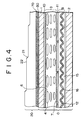
- the light guide plate 20 has separated band plane portions 22 and slant portions 21 located between respective plane portions 22. The illumination light guided from the light source 30 is reflected on the slant portions 21 and comes into the first substrate 1, and the illumination light reflected from the second substrate 2 comes out from the plane portions 22.
- Fig. 2 is a schematic cross sectional view for illustrating a reference example of a reflective display.
- This reference example shows comparison in order to clarify the usefulness of the present invention.
- a light guide plate 20 and a first substrate 1 of a panel 0 are bonded each other with interposition of a transparent interposition layer 40 made of, for example, resin. Unnecessary reflection of the illumination light and outside light on the interface between the light guide plate 20 and the first substrate 1 is suppressed by setting adequately the refractive index of the interposition layer 40.
- the interposition layer 40 is used instead of the laminate structure of the polarization plate and the quarter wavelength plate in order to suppress the unnecessary reflection.
- the interposition layer 40 may consist of, for example, an adhesive transparent resin.
- a transparent resin is coated on the surface of the first substrate 1 of the panel, and a light guide plate 20 is adhered on it. It is required to match optically in order to suppress unnecessary reflection, the resin of the interposition layer 40 and the resin of the light guide plate 20 and the first substrate 1 are selected so that the refractive index of these resins are approximately equal.
- the refractive index of the resin which forms the interposition layer 40 should be approximately 1.5.
- the resin with a low viscosity is desirably used.
- Figs. 3A to 3C show the detailed structure of the light guide plate 20 shown in Fig. 2.
- Fig. 3A shows a plane view
- Fig. 3B shows a cross sectional view
- Fig. 3C shows an enlarged cross sectional view.
- the bottom side 28 of the sheet-like light guide plate 20 is bonded on the panel 0.
- adhesive resin stuck on the end 25, upper surface 26, and side surface 27 of the light guide plate 20 the optical function may be degraded. Therefore, when the light guide plate 20 and the panel 0 are bonded together with an ultra-violet curing resin, it is required to cover the end 25, upper surface 26, and side surface 27 of the light guide plate 20 with a tape. After bonding, the light guide plate 20 and the panel 0 are combined together.
- the light guide plate is installed on the front surface of the panel, if an air layer is interposed between the light guide plate and the panel, because the refractive index of air is not equal to that of the light guide plate and also is not equal to that of the panel, the incident light is reflected approximately 10 %. Such reflected light is not involved in electro-optical switching of the panel, therefore makes the contrast of the reflective display very poor.
- the light guide plate and the panel are bonded together with a transparent resin having the refractive index approximately equal to those of the light guide plate and the panel.
- such bonding work is troublesome, and results in complex manufacturing process and reduced manufacturing yield.
- Fig. 4 is a partial cross sectional view for illustrating a detailed example of the reflective display in accordance with the present invention. Components corresponding to those of the embodiment shown in Fig. 1 are given the same reference characters as shown in Fig. 1 for easy understanding.
- a TN-ECB Transist Nematic-Electrically Controlled Birefringence
- this reflective display has the structure in which the independent light guide plate 20 and panel 0 are combined together. The slant portion 21 and the plane portion 22 are formed on the surface of the light guide plate 20.
- the light guide plate 20 has a size of, for example, 90 x 120 mm, the thickness of the end on the side near the light source is, for example, 3.2 mm, and the thickness of the end on the side opposite to the light source is 0.2 mm.
- the light guide plate consists of, for example, transparent acrylic board, and the slant portion 21 and the plane portion 22 are subjected to machine work with a diamond cutter having an inclination angle of 135 degrees.
- the location period of the slant portion 21 is, for example, 120 ⁇ m.
- the polarization plate 70 and the quarter wavelength plate 80 are attached on the back side of the light guide plate 20.
- the light guide plate 20 having the laminate structure as described herein above is placed on the surface of the panel 0.
- the panel 0 is a component formed by bonding the first substrate 1 made of, for example, a transparent glass plate located on the incident side of the outside light on the second substrate 2 located on the opposite side with interposition of a prescribed space.
- the nematic liquid crystal layer 3, for example, is held in the space between both substrates 1 and 2.
- the liquid crystal molecules 4 is twist oriented by the top and bottom orientation films 6 and 7.
- Electrodes 10 and 11 are formed on the inside surface of respective substrates 1 and 2, and a voltage is applied to the nematic liquid crystal layer 3 on every pixel.
- the electrode 10 formed on the first substrate 1 is patterned in the form of stripe
- the electrode 11, made of ITO for example, formed on the second substrate 2 is patterned in the form of stripe.
- Both electrodes 10 and 11 are disposed orthogonally each other, and form a so-called simple matrix on which a pixel is formed on each intersection.
- the reflection liquid crystal display apparatus having the structure as described herein above is a TN-ECB type normally white mode apparatus.
- the nematic liquid crystal layer 3 holds twist orientation and functions as a quarter wavelength plate when no voltage is applied, and allows the outside light to pass and displays white cooperatively with the polarization plate 70 and the quarter wavelength plate 80. When a voltage is applied, the nematic liquid crystal layer 3 changes to perpendicular orientation and loses the function of a quarter wavelength plate, and shuts the outside light and displays black cooperatively with the polarization plate 70 and the quarter wavelength plate 80.
- the polarization plate 70 is placed over the surface of the first substrate 1 of the panel 0.
- the quarter wavelength plate 80 is interposed between the polarization plate 70 and the first substrate 1.
- the quarter wavelength plate 80 comprises, for example, stretched polymer film, and gives a phase difference corresponding to a quarter wavelength between the ordinary light and extraordinary light.
- the optical axis (one anisotropic axis) of the quarter wavelength plate 80 is oriented so as to make an angle of 45 degrees to the polarization axis (transmission axis) of the polarization plate 70.
- the outside light becomes a linearly polarized light after transmission through the polarization plate 70.
- the linearly polarized light becomes a circularly polarized light after transmission through the quarter wavelength plate 80.
- the circularly polarized light becomes a linearly polarized light again after transmission through the quarter wavelength plate.
- the polarization direction turns 90 degrees from the original polarization direction.
- the quarter wavelength plate is capable of turning the polarization direction by combining with the polarization plate, and this phenomenon is used for display.
- the panel 0 uses the nematic liquid crystal layer 3 consisting of nematic liquid crystal molecules 4 having basically positive horizontally oriented dielectric anisotropy as the electro-optical material.
- the nematic liquid crystal layer 3 having a suitable thickness functions as a quarter wavelength plate.
- refractive index anisotropy ⁇ n of the nematic liquid crystal layer 3 is approximately 0.7, and the thickness of the nematic liquid crystal layer 3 is, for example, approximately 3 ⁇ m. Therefore, the retardation ⁇ n ⁇ d of the nematic liquid crystal layer 3 ranges from 0.2 to 0.25 ⁇ m.
- the above-mentioned retardation value becomes approximately 0.15 ⁇ m (150 nm) substantially by twist orientation of the nematic liquid crystal molecules 4.
- This value corresponds approximately to 1/4 median wavelength (approximately 600 nm) of the outside light, and the nematic liquid crystal layer 3 is capable of functioning optically as a quarter wavelength plate.
- the nematic liquid crystal layer 3 is placed between the top and bottom orientation films 6 and 7 made of, for example, polyimide to obtain desired twist orientation.
- the liquid crystal molecules 4 are arranged along the rubbing direction of the orientation film 6 on the first substrate 1 side, and the liquid crystal molecules 4 are arranged along the rubbing direction of the orientation film 7 on the second substrate 2 side.
- the rubbing direction of the orientation film 6 and the orientation film 7 is deviated by 60 to 70 degrees each other to obtain the desired twist orientation.
- the light reflection layer 8 is formed under the electrode 11 on the second substrate 2 side.
- the light reflection layer 8 has convexes and concaves on the surface and scatters the light. Therefore, the appearance is paper white, which is preferable as display background, and because the light reflection layer 8 reflects the incident light in the relatively wide angle range, the wide visible angle is realized for easy viewing of the display and the brightness of the display increases in the wide angle of view range.
- the transparent planarization layer 12 made of, for example, acrylic resin is interposed between the light reflection layer 8 and the electrode 11 to planarize the convexes and concaves.
- the light reflection layer 8 comprises a resin film 15 shaped in the form of convex and concave and a metal film 16 consisting of aluminum formed on the surface of the resin film 15.
- the resin film 15 is a photo-sensitive resin film patterned in the form of convex and concave by means of photo-lithography.
- the photo-sensitive resin film 15 consists of, for example, photo-resist which are coated over the entire surface of the substrate.
- the photo-resist is exposed to the light with interposition of a desired mask to pattern in the form of, for example, cylinder.
- the photo-resist is subjected to heating and reflow to form stably convexes and concaves.
- the metal film 16 with a desired thickness, made of, for example, aluminum, which has good reflectance, is formed on the convex and concave surface formed as described herein above.
- the planarization layer 12 is formed to planarize the convex and concave surface.
- the planarization layer 12 consists desirably of transparent organic substance such as acrylic resin. The interposition of the planarization layer 12 helps the electrode 11 and the orientation film 7 to be formed stably.
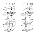
- this reflective display has the structure that the polarization plate 70, the quarter wavelength plate 80, the nematic liquid crystal layer 3, and the light reflection layer 8 are placed on one another in the order in the view from an observer.
- the light guide plate is omitted for easy understanding.
- the polarization axis (transmission axis) of the polarization plate 70 is represented with 70P.
- the optical axis 80S of the quarter wavelength plate 80 makes an angle of 45 degrees to the transmission axis 70P.
- the orientation direction 3R of the liquid crystal molecules 4 of the first substrate side is parallel to the polarization axis (transmission axis) of the polarization plate 70.
- the incident light 201 becomes a linearly polarized light 202 after transmission through the polarization plate 70.
- the polarization direction is parallel to the transmission axis 70P, and the linearly polarized light 202 is referred to as parallel linearly polarized light hereinafter.
- the parallel linearly polarized light 202 is converted to a circularly polarized light 203 after transmission through the quarter wavelength plate 80.
- the circularly polarized light 203 is converted to a linearly polarized light after transmission through the nematic liquid crystal layer 3 which functions as a quarter wavelength plate.
- the polarization direction of the linearly polarized light is turned 90 degrees and intersects with the parallel linearly polarized light 202 perpendicularly.
- orthogonal linearly polarized light turned 90 degrees is referred to as orthogonal linearly polarized light.
- the orthogonal linearly polarized light 203 is reflected on the light reflection layer 8, and passes again through the nematic liquid crystal layer 3 which functions as a quarter wavelength plate 80, when the orthogonal linearly polarized light 203 is converted to a circularly polarized light 204. Further the circularly polarized light 204 passes through the quarter wavelength plate 80, when the circularly polarized light 204 is converted to an original parallel linearly polarized light 205.
- the parallel linearly polarized light 205 passes through the polarization plate 70 and is converted to a coming out light 206, which is viewed by an observer, and white display is obtained.
- the liquid crystal molecules 4 are shifted from twist orientation to perpendicular orientation, and the quarter wavelength plate function is lost.
- the outside light 201 which passes the polarization plate 80 is converted to a parallel linearly polarized light 202.
- the parallel linearly polarized light 202 is converted to a circularly polarized light 203 when the parallel linearly polarized light 202 passes through the quarter wavelength plate 80.
- the circularly polarized light 203 passes through the nematic liquid crystal layer 3 as it is, is reflected on the light reflection layer 8, and comes to the quarter wavelength plate 80 as the circularly polarized light 204a.
- the circularly polarized light 204a is converted to an orthogonal linearly polarized light 205a when the circularly polarized light 203 passes through the quarter wavelength plate 80. Because the orthogonal linearly polarized light 205a can not pass the polarization plate 70, the display turns to black.
- the reflective display has a structure comprising the polarization plate 70, the quarter wavelength plate 80, the first substrate 1, the electrode 10, the liquid crystal layer 3, the planarization layer 12, the light reflection layer 8, and the second substrate 2 laminated in this order from the top.
- the light guide plate is omitted from the drawing.
- the light reflection layer 8 serves also as the electrode 11.
- the electrode 11 is divided into the matrix form, and functions as the pixel electrode. Individual electrodes are driven by the thin film transistor 50 consisting of, for example, polysilicon, and form a so-called active matrix type display apparatus.
- the transmission axis of the polarization plate 70 is shown by the stripe pattern as shown in the drawing.
- the optical axis of the quarter wavelength plate 80 makes a angle of 45 degrees to the transmission axis (polarization axis) of the polarization plate 70.
- the liquid crystal layer 3 functions as a quarter wavelength plate in OFF state.
- the incident light such as illumination light or outside light is converted to a parallel linearly polarized light when the incident light passes though the polarization plate 70.
- the parallel linearly polarized light is converted to a circularly polarized light when the parallel linearly polarized light passes through the quarter wavelength plate 80.
- the circularly polarized light is converted to an orthogonal linearly polarized light when the circularly polarized light passes the liquid crystal layer 3.
- the orthogonal linearly polarized light is reflected on the light reflection layer 8, converted to a circularly polarized light by the liquid crystal layer 3, and further converted to a parallel linearly polarized light by the quarter wavelength plate 80. Therefore, the parallel linearly polarized light passes through the polarization plate 70 without changing and comes to an observer as a coming out light.
- the incident light converted to the circularly polarized light by the quarter wavelength plate 80 is partially mirror reflected on the interface between the electrode 10 and the substrate 1.
- the mirror reflected unnecessary circularly polarized light is converted to an orthogonal linearly polarized light by the quarter wavelength plate 80.
- the orthogonal linearly polarized light reflected on the interface is absorbed because the polarization plane is orthogonal to the transmission axis.
- a light guide plate is used in the present invention as described herein above.
- a typical structure of a light guide plate is shown in Fig. 7.
- the light guide plate 20 is placed on the glass substrate on the front side of the reflection panel.
- the light guide plate 20 comprises, for example, slant portions 21 having a slant angle of 45 degrees and plane portions 22 which are parallel to the glass substrate of the panel, and forms a diffraction grating having a periodical structure.
- Fig. 8 is a schematic diagram for illustrating a reference example in which the light guide plate 20 shown in Fig. 7 is bonded to the panel 0 with a transparent interposition layer 40.
- a light source comprising, for example, a cold cathode tube is provided near the end 25 of the light guide plate 20.
- the illumination light emitted from the cold cathode tube is incident horizontally from the end 25 and totally reflected perpendicularly downward on the slant portions 21 having a slant angle of 45 degrees.
- the reflected light illuminates the reflection panel 0 from the front side.
- the image screen is viewed with illumination of environment (outside light) in a bright environment, on the other hand, in a dark environment, the cold cathode tube is lighted to illuminate the panel 0, and the image screen is viewed.
- environment outside light
- the cold cathode tube is lighted to illuminate the panel 0
- the image screen is viewed.
- the light guide plate 20 is located directly on the front side of the reflection panel, the image screen is viewed not clearly because of generation of interference fringe due to the periodical structure of the light guide plate 20.
- the illumination light emitted from the light source is totally reflected perpendicularly downward by the light guide plate 20, the illumination light is subjected to diffraction due to the periodical structure of the light guide plate 20, and the first order light, second order light, Vietnamese are generated in addition to the zero order light.
- the illumination light reflected from the panel 0 passes again the light guide plate 20, where, the illumination light is subjected to diffraction, and the zero order light, the first order light, ... are generated.
- the zero order light and the first order light generated from two diffractions interfere with each other.
- bright and dark stripe pattern is viewed with overlapping on the image screen.
- the stripe pattern causes unclear visibility of the display.
- the interference fringe becomes remarkable.
- the interference fringe becomes remarkable.
- the interference fringe becomes remarkable.
- the interference fringe becomes remarkable.
- the visual line of an observer is inclined to the side facing to the slant plane of the slant portions 21, the interference fringe becomes remarkable.
- the larger the inclination of the visual line the clearer the interference fringe (moiré) becomes.
- Figs. 9A and 9B show schematically generation of moiré.
- Fig. 9A is a drawing with addressing on unnecessary illumination light reflected on the interface 1/10 between the first substrate 1 consisting of glass and the electrode 10 comprising a transparent conductive film consisting of ITO.
- Fig. 9B is a drawing with addressing on the primary illumination light reflected on the light reflection layer 8 formed on the second substrate.
- the light guide plate 20 is folded with respect to the reflection plane for easy understanding.
- the light guide plate 20 functions as a sort of diffraction grating 201 because the slant portions 21 and plane portions 22 are arranged periodically.
- the illumination light which has passed the diffraction grating 201 is subjected to mirror reflection on the interface 1/10 and passes again through the light guide plate 20.
- the light guide plate 20 functions as a diffraction grating 202.
- a pair of diffraction gratings 201 and 202 are complementary to each other. Equivalently, as the result, the illumination light passes the diffraction gratings 201 and 202, and reaches an observer.
- the first order diffracted light and the second order diffracted light interfere with each other to form a moiré.
- the illumination light is divided into the zero order diffracted light and the first order diffracted light by the diffraction grating 201.
- These diffracted lights are subjected again to diffraction by the diffraction grating 202, and divided to the zero order diffracted light and the first order diffracted light.
- the first order diffracted light generated from the first zero order diffracted light and the zero order diffracted light generated from the first order diffracted light interfere strongly with each other because the total of the order is equal to each other.
- the parallel incident light from the cold cathode tube is reflected by the slant portions 21 of the light guide plate, and proceeds to the interface 1/10 as it is.
- the light subjected to mirror reflection on the interface is a parallel light.
- the parallel incident light and the parallel reflected light interfere with each other because these lights pass the nearly same path. This interference is the cause of moiré.
- the illumination light reflected on the light reflection layer 8 which scatters the light in nature is not involved in interference.
- the illumination light reflected on the light reflection layer 8 contains the zero order diffracted light and the first order diffracted light mixedly, is not involved in interference, and causes no moiré pattern.
- the laminate structure comprising the polarization plate 70 and the quarter wavelength plate 80 is attached on the back side of the light guide plate 20.
- the polarization plate 70 and the quarter wavelength plate 80 function cooperatively to suppress unnecessary reflection of the illumination light on the electrode 10. As a result, it is possible to remove substantially the moiré due to the periodical structure of the light guide plate 20.
- a light guide plate is placed on the reflection type panel and an auxiliary illumination light source is provided on the end of the light guide plate.
- the light guide plate allows normally the outside light to be transmitted, which is incident on the panel, and allows the outside light reflected on the panel to come out
- the light guide panel guides the illumination light as required, which is incident on the panel, and allows the illumination light reflected on the panel to come out.
- An image is observable in a dark environment though this is a reflection type panel by lighting the light source.
- the light source is turned off to save the power.
- a laminate structure comprising a polarization plate and a quarter wavelength plate is attached on the back side of the light guide plate to shut off unnecessary reflection of the panel, and thus the quality of a display screen is improved.
Landscapes
- Physics & Mathematics (AREA)
- Nonlinear Science (AREA)
- General Physics & Mathematics (AREA)
- Optics & Photonics (AREA)
- Chemical & Material Sciences (AREA)
- Crystallography & Structural Chemistry (AREA)
- Liquid Crystal (AREA)
- Mathematical Physics (AREA)
- Devices For Indicating Variable Information By Combining Individual Elements (AREA)
Applications Claiming Priority (2)
| Application Number | Priority Date | Filing Date | Title |
|---|---|---|---|
| JP07669898 | 1998-03-10 | ||
| JP10076698A JPH11259007A (ja) | 1998-03-10 | 1998-03-10 | 反射型表示装置 |
Publications (1)
| Publication Number | Publication Date |
|---|---|
| EP0942228A1 true EP0942228A1 (fr) | 1999-09-15 |
Family
ID=13612728
Family Applications (1)
| Application Number | Title | Priority Date | Filing Date |
|---|---|---|---|
| EP99400585A Withdrawn EP0942228A1 (fr) | 1998-03-10 | 1999-03-10 | Affichage réflectif |
Country Status (4)
| Country | Link |
|---|---|
| US (1) | US6108059A (fr) |
| EP (1) | EP0942228A1 (fr) |
| JP (1) | JPH11259007A (fr) |
| KR (1) | KR19990077709A (fr) |
Cited By (3)
| Publication number | Priority date | Publication date | Assignee | Title |
|---|---|---|---|---|
| EP1130454A3 (fr) * | 2000-02-29 | 2001-10-17 | Alps Electric Co., Ltd. | Dispositif d'affichage à cristaux liquides dans lequel la génération des franges de Moiré est inhibée |
| EP1359460A3 (fr) * | 2002-04-26 | 2004-01-14 | Optrex Corporation | Dispositif d'affichage à cristal liquide nématique du type double couche et procédé pour l'inspection de substrats transparents |
| CN104282225A (zh) * | 2013-07-01 | 2015-01-14 | 元太科技工业股份有限公司 | 显示装置 |
Families Citing this family (105)
| Publication number | Priority date | Publication date | Assignee | Title |
|---|---|---|---|---|
| JPH11281979A (ja) * | 1998-03-26 | 1999-10-15 | Enplas Corp | サイドライト型面光源装置及び液晶表示装置 |
| JPH11297115A (ja) * | 1998-04-14 | 1999-10-29 | Nitto Denko Corp | 導光板、面光源装置及び反射型液晶表示装置 |
| JP3410977B2 (ja) * | 1998-09-14 | 2003-05-26 | シャープ株式会社 | フロントライト及び反射型液晶表示装置 |
| JP2000111900A (ja) * | 1998-10-02 | 2000-04-21 | Sony Corp | 反射型表示装置 |
| CA2290860C (fr) * | 1998-11-27 | 2007-05-22 | National Research Council Of Canada | Systeme d'eclairage polarisant en contre-jour pour ecrans a cristaux liquides a vision directe |
| US6392727B1 (en) * | 1998-12-31 | 2002-05-21 | Honeywell International Inc. | Reduced reflectance polarized display |
| US6421104B1 (en) * | 1999-10-22 | 2002-07-16 | Motorola, Inc. | Front illuminator for a liquid crystal display and method of making same |
| JP4197813B2 (ja) * | 1999-11-02 | 2008-12-17 | 日東電工株式会社 | 液晶表示装置 |
| KR100771258B1 (ko) * | 2000-05-09 | 2007-10-29 | 가부시키가이샤 한도오따이 에네루기 켄큐쇼 | 본인 인증 시스템과 본인 인증 방법 및 휴대 전화 장치 |
| US6352350B1 (en) * | 2000-06-01 | 2002-03-05 | Agilent Technologies, Inc. | High efficiency flat illuminator for liquid crystal micro-display |
| KR20020001594A (ko) * | 2000-06-26 | 2002-01-09 | 가마이 고로 | 도광판, 면광원 장치 및 반사형 액정 표시 장치 |
| US6592233B1 (en) * | 2000-10-03 | 2003-07-15 | Nokia Mobile Phones Ltd. | Lighting device for non-emissive displays |
| JP2002148615A (ja) * | 2000-11-08 | 2002-05-22 | Nitto Denko Corp | 光学フィルム及び反射型液晶表示装置 |
| JP3871913B2 (ja) * | 2000-11-14 | 2007-01-24 | シャープ株式会社 | 反射型表示装置およびプリズムアレイシート |
| JP2002169149A (ja) | 2000-12-01 | 2002-06-14 | Mitsubishi Electric Corp | 反射型液晶表示装置 |
| JP2003029258A (ja) * | 2001-07-19 | 2003-01-29 | Omron Corp | 反射型表示装置及び携帯情報機器 |
| JP3702823B2 (ja) * | 2001-08-23 | 2005-10-05 | セイコーエプソン株式会社 | 液晶表示装置および電子機器 |
| JP4166455B2 (ja) * | 2001-10-01 | 2008-10-15 | 株式会社半導体エネルギー研究所 | 偏光フィルム及び発光装置 |
| JP2003131582A (ja) * | 2001-10-22 | 2003-05-09 | Minebea Co Ltd | 表示装置 |
| JP3980890B2 (ja) * | 2002-01-23 | 2007-09-26 | シャープ株式会社 | 導光板並びにそれを備えた光源装置及び表示装置 |
| JP3719436B2 (ja) * | 2002-03-06 | 2005-11-24 | セイコーエプソン株式会社 | 電気光学装置、および電子機器 |
| JP2003279950A (ja) * | 2002-03-25 | 2003-10-02 | Sharp Corp | 表示装置 |
| JP2004095390A (ja) * | 2002-08-30 | 2004-03-25 | Fujitsu Display Technologies Corp | 照明装置及び表示装置 |
| US7063449B2 (en) * | 2002-11-21 | 2006-06-20 | Element Labs, Inc. | Light emitting diode (LED) picture element |
| JP4294992B2 (ja) * | 2003-03-31 | 2009-07-15 | シャープ株式会社 | 反射型液晶表示装置 |
| CN100437207C (zh) * | 2004-03-31 | 2008-11-26 | 松下电器产业株式会社 | 颜色分离装置及摄像装置 |
| TWI240124B (en) * | 2004-05-31 | 2005-09-21 | Au Optronics Corp | Display device and electronic device utilizing the same |
| TWI233220B (en) * | 2004-06-18 | 2005-05-21 | Chi Mei Optoelectronics Corp | Light emitting diode package |
| KR20060001251A (ko) * | 2004-06-30 | 2006-01-06 | 엘지.필립스 엘시디 주식회사 | 백 라이트 유닛 |
| KR100661365B1 (ko) * | 2005-04-27 | 2006-12-27 | 삼성전자주식회사 | 액정표시장치 |
| DE102006007065A1 (de) * | 2006-02-15 | 2007-08-16 | BSH Bosch und Siemens Hausgeräte GmbH | Vorrichtung zur Hintergrundbeleuchtung einer LC-Anzeigeeinrichtung für eine Anzeige- und/oder Bedienungseinheit, insbesondere in einem Hausgerät |
| US9040808B2 (en) * | 2007-05-01 | 2015-05-26 | Morgan Solar Inc. | Light-guide solar panel and method of fabrication thereof |
| US9337373B2 (en) | 2007-05-01 | 2016-05-10 | Morgan Solar Inc. | Light-guide solar module, method of fabrication thereof, and panel made therefrom |
| US7873257B2 (en) * | 2007-05-01 | 2011-01-18 | Morgan Solar Inc. | Light-guide solar panel and method of fabrication thereof |
| US7672549B2 (en) * | 2007-09-10 | 2010-03-02 | Banyan Energy, Inc. | Solar energy concentrator |
| US8412010B2 (en) | 2007-09-10 | 2013-04-02 | Banyan Energy, Inc. | Compact optics for concentration and illumination systems |
| KR101455892B1 (ko) * | 2007-09-10 | 2014-11-04 | 반얀 에너지, 인크 | 광 에너지의 집광, 집결 및 조명을 위한 소형 광소자 |
| JP4656176B2 (ja) * | 2008-04-11 | 2011-03-23 | ソニー株式会社 | 導光板、表示装置、及び表示器付き電子機器 |
| KR101127581B1 (ko) * | 2009-12-18 | 2012-03-26 | 삼성모바일디스플레이주식회사 | 백라이트 유니트 및 이를 채용한 디스플레이 모듈 |
| JP5516319B2 (ja) * | 2010-10-20 | 2014-06-11 | ソニー株式会社 | 照明装置および表示装置 |
| CN103238091A (zh) | 2010-10-28 | 2013-08-07 | 榕树能量公司 | 用于聚集和照明系统的变向光学装置 |
| SG190160A1 (en) | 2010-11-19 | 2013-06-28 | Reald Inc | Directional flat illuminators |
| US9250448B2 (en) | 2010-11-19 | 2016-02-02 | Reald Inc. | Segmented directional backlight and related methods of backlight illumination |
| US20140041205A1 (en) | 2010-11-19 | 2014-02-13 | Reald Inc. | Method of manufacturing directional backlight apparatus and directional structured optical film |
| US8651726B2 (en) | 2010-11-19 | 2014-02-18 | Reald Inc. | Efficient polarized directional backlight |
| US8885995B2 (en) | 2011-02-07 | 2014-11-11 | Morgan Solar Inc. | Light-guide solar energy concentrator |
| US10288254B2 (en) * | 2011-02-25 | 2019-05-14 | 3M Innovative Properties Company | Front-lit reflective display device |
| TWI556971B (zh) * | 2011-04-13 | 2016-11-11 | Lg化學股份有限公司 | 光學薄膜 |
| WO2012158574A1 (fr) * | 2011-05-13 | 2012-11-22 | Reald Inc. | Rétroéclairage directionnel polarisé et efficace |
| WO2013028467A1 (fr) | 2011-08-19 | 2013-02-28 | Barnesandnoble.Com Llc | Système d'éclairage frontal plan possédant un guide de lumière sur lequel sont formés des éléments de microdiffusion et son procédé de fabrication |
| GB2507453A (en) * | 2011-08-19 | 2014-04-30 | Barnesandnoble Com Llc | Planar front illumination system having a light guide with micro lenses formed thereon and method of manufacturing the same |
| US9237337B2 (en) | 2011-08-24 | 2016-01-12 | Reald Inc. | Autostereoscopic display with a passive cycloidal diffractive waveplate |
| US9436015B2 (en) | 2012-12-21 | 2016-09-06 | Reald Inc. | Superlens component for directional display |
| US10054732B2 (en) | 2013-02-22 | 2018-08-21 | Reald Spark, Llc | Directional backlight having a rear reflector |
| TWI467280B (zh) * | 2011-12-08 | 2015-01-01 | E Ink Holdings Inc | 反射式顯示器 |
| US8328403B1 (en) | 2012-03-21 | 2012-12-11 | Morgan Solar Inc. | Light guide illumination devices |
| US9188731B2 (en) | 2012-05-18 | 2015-11-17 | Reald Inc. | Directional backlight |
| JP6189423B2 (ja) | 2012-05-18 | 2017-08-30 | リアルディー スパーク エルエルシー | 指向性光源用制御システム |
| US9709723B2 (en) | 2012-05-18 | 2017-07-18 | Reald Spark, Llc | Directional backlight |
| WO2013173732A1 (fr) | 2012-05-18 | 2013-11-21 | Reald Inc. | Agencement de guide d'onde éclairé de façon directionnelle |
| TWI636283B (zh) | 2012-05-18 | 2018-09-21 | 美商瑞爾D斯帕克有限責任公司 | 定向背光源、定向顯示裝置及其光源陣列的控制方法 |
| US9350980B2 (en) | 2012-05-18 | 2016-05-24 | Reald Inc. | Crosstalk suppression in a directional backlight |
| US9235057B2 (en) | 2012-05-18 | 2016-01-12 | Reald Inc. | Polarization recovery in a directional display device |
| US9678267B2 (en) | 2012-05-18 | 2017-06-13 | Reald Spark, Llc | Wide angle imaging directional backlights |
| US8917441B2 (en) | 2012-07-23 | 2014-12-23 | Reald Inc. | Observe tracking autostereoscopic display |
| CN104823097A (zh) | 2012-10-02 | 2015-08-05 | 瑞尔D股份有限公司 | 使用反射定向元件的阶梯式波导自动立体显示装置 |
| CN110234000B (zh) | 2013-06-17 | 2021-07-13 | 瑞尔D斯帕克有限责任公司 | 远程会议方法和远程通信系统 |
| WO2015057625A1 (fr) | 2013-10-14 | 2015-04-23 | Reald Inc. | Commande d'affichage directionnel |
| US9739928B2 (en) | 2013-10-14 | 2017-08-22 | Reald Spark, Llc | Light input for directional backlight |
| WO2015073438A1 (fr) | 2013-11-15 | 2015-05-21 | Reald Inc. | Rétroéclairages directionnels avec des boîtiers d'éléments émetteurs de lumière |
| CN106662773B (zh) | 2014-06-26 | 2021-08-06 | 瑞尔D 斯帕克有限责任公司 | 定向防窥显示器 |
| US10175519B2 (en) * | 2014-09-02 | 2019-01-08 | Sharp Kabushiki Kaisha | Mirror display having touch panel |
| WO2016057690A1 (fr) | 2014-10-08 | 2016-04-14 | Reald Inc. | Rétroéclairage directionnel |
| WO2016105541A1 (fr) | 2014-12-24 | 2016-06-30 | Reald Inc. | Réglage de la rotondité perçue dans une image stéréoscopique d'une tête |
| CN104615397A (zh) * | 2015-02-02 | 2015-05-13 | 广东小天才科技有限公司 | 一种用于移动终端的低功耗的显示装置及其控制方法 |
| RU2596062C1 (ru) | 2015-03-20 | 2016-08-27 | Автономная Некоммерческая Образовательная Организация Высшего Профессионального Образования "Сколковский Институт Науки И Технологий" | Способ коррекции изображения глаз с использованием машинного обучения и способ машинного обучения |
| DE102015104299A1 (de) | 2015-03-23 | 2016-09-29 | International Automotive Components Group Gmbh | Innenverkleidungsteil für ein Kraftfahrzeug |
| EP3283906B1 (fr) | 2015-04-13 | 2020-09-23 | RealD Spark, LLC | Dispositifs de rétroéclairage directionnel d'imagerie à grand angle |
| EP3304188B1 (fr) | 2015-05-27 | 2020-10-07 | RealD Spark, LLC | Rétroéclairages directionnels d'imagerie à grand angle |
| EP3369034B1 (fr) | 2015-10-26 | 2023-07-05 | RealD Spark, LLC | Système de confidentialité intelligent, appareil et procédé associés |
| US10459321B2 (en) | 2015-11-10 | 2019-10-29 | Reald Inc. | Distortion matching polarization conversion systems and methods thereof |
| US10330843B2 (en) | 2015-11-13 | 2019-06-25 | Reald Spark, Llc | Wide angle imaging directional backlights |
| EP4293417A3 (fr) | 2015-11-13 | 2024-01-24 | RealD Spark, LLC | Éléments de surface pour rétroéclairages directionnels d'imagerie |
| JP2017111267A (ja) * | 2015-12-16 | 2017-06-22 | 富士フイルム株式会社 | 車両用画像表示機能付きミラーおよびその製造方法 |
| EP3400706B1 (fr) | 2016-01-05 | 2022-04-13 | RealD Spark, LLC | Correction du regard d'images multi-vues |
| WO2017200950A1 (fr) | 2016-05-19 | 2017-11-23 | Reald Spark, Llc | Rétroéclairages directionnels d'imagerie à grand angle |
| WO2017205183A1 (fr) | 2016-05-23 | 2017-11-30 | Reald Spark, Llc | Rétroéclairages directionnels d'imagerie à grand angle |
| CN110178072B (zh) | 2017-01-04 | 2022-03-11 | 瑞尔D斯帕克有限责任公司 | 用于成像定向背光源的光学叠堆 |
| WO2018187154A1 (fr) | 2017-04-03 | 2018-10-11 | Reald Spark, Llc | Rétroéclairages directionnels d'imagerie segmentée |
| US10126575B1 (en) | 2017-05-08 | 2018-11-13 | Reald Spark, Llc | Optical stack for privacy display |
| US10303030B2 (en) | 2017-05-08 | 2019-05-28 | Reald Spark, Llc | Reflective optical stack for privacy display |
| US11327358B2 (en) | 2017-05-08 | 2022-05-10 | Reald Spark, Llc | Optical stack for directional display |
| EP4293574A3 (fr) | 2017-08-08 | 2024-04-03 | RealD Spark, LLC | Ajustement d'une représentation numérique d'une région de tête |
| JP7005243B2 (ja) * | 2017-09-14 | 2022-01-21 | 株式会社ジャパンディスプレイ | 表示装置 |
| TWI878209B (zh) | 2017-09-15 | 2025-04-01 | 美商瑞爾D斯帕克有限責任公司 | 顯示裝置及應用於顯示裝置的視角控制光學元件 |
| US11115647B2 (en) | 2017-11-06 | 2021-09-07 | Reald Spark, Llc | Privacy display apparatus |
| EP3743766B1 (fr) | 2018-01-25 | 2026-02-11 | RealD Spark, LLC | Écran tactile pour affichage de confidentialité |
| TWI827580B (zh) | 2018-01-25 | 2024-01-01 | 美商瑞爾D斯帕克有限責任公司 | 用於防窺顯示裝置之反射式光學堆疊物 |
| CN111736254B (zh) * | 2020-07-24 | 2022-11-04 | 京东方科技集团股份有限公司 | 一种显示装置及其制备方法 |
| CN116194812A (zh) | 2020-09-16 | 2023-05-30 | 瑞尔D斯帕克有限责任公司 | 车辆外部照明装置 |
| US12585094B2 (en) | 2022-06-22 | 2026-03-24 | Reald Spark, Llc | Anamorphic directional illumination device |
| WO2024030274A1 (fr) | 2022-08-02 | 2024-02-08 | Reald Spark, Llc | Affichage proche de l'œil de suivi de pupille |
| US12282168B2 (en) | 2022-08-11 | 2025-04-22 | Reald Spark, Llc | Anamorphic directional illumination device with selective light-guiding |
| US12099271B1 (en) * | 2023-07-19 | 2024-09-24 | Volkswagen Aktiengesellschaft | Controllable light propagation system |
| TWI882470B (zh) * | 2023-10-13 | 2025-05-01 | 中強光電股份有限公司 | 顯示裝置 |
Citations (4)
| Publication number | Priority date | Publication date | Assignee | Title |
|---|---|---|---|---|
| US4492432A (en) * | 1980-07-28 | 1985-01-08 | Bbc Brown, Boveri & Company, Limited | Homeotropic nematic display with internal reflector |
| EP0545705A1 (fr) * | 1991-12-03 | 1993-06-09 | Sharp Kabushiki Kaisha | Dispositif d'affichage à cristal liquide |
| WO1993016410A1 (fr) * | 1992-02-14 | 1993-08-19 | Raychem Corporation | Affichage a cristaux liquides eclaire a l'avant |
| EP0770818A2 (fr) * | 1995-10-24 | 1997-05-02 | SHARP Corporation | Dispositif d'illumination |
Family Cites Families (9)
| Publication number | Priority date | Publication date | Assignee | Title |
|---|---|---|---|---|
| DE3573649D1 (en) * | 1984-07-02 | 1989-11-16 | Mitsubishi Rayon Co | Light diffuser |
| US5050946A (en) * | 1990-09-27 | 1991-09-24 | Compaq Computer Corporation | Faceted light pipe |
| TW594115B (en) * | 1992-10-09 | 2004-06-21 | Asahi Glass Co Ltd | A liquid crystal display device and an illumination device for a direct viewing type display element |
| US5418631A (en) * | 1993-05-14 | 1995-05-23 | Kaiser Optical Systems, Inc. | Edge-lit holographic diffusers for flat-panel displays |
| US5485354A (en) * | 1993-09-09 | 1996-01-16 | Precision Lamp, Inc. | Flat panel display lighting system |
| US5982540A (en) * | 1994-03-16 | 1999-11-09 | Enplas Corporation | Surface light source device with polarization function |
| JP3219943B2 (ja) * | 1994-09-16 | 2001-10-15 | 株式会社東芝 | 平面直視型表示装置 |
| JP2915317B2 (ja) * | 1995-02-28 | 1999-07-05 | インターナショナル・ビジネス・マシーンズ・コーポレイション | 導光体ユニット、液晶表示装置及び偏光方法 |
| JPH11133412A (ja) * | 1997-10-29 | 1999-05-21 | Nitto Denko Corp | 液晶素子、光学素子及び偏光素子 |
-
1998
- 1998-03-10 JP JP10076698A patent/JPH11259007A/ja active Pending
-
1999
- 1999-03-08 US US09/264,242 patent/US6108059A/en not_active Expired - Lifetime
- 1999-03-09 KR KR1019990007733A patent/KR19990077709A/ko not_active Ceased
- 1999-03-10 EP EP99400585A patent/EP0942228A1/fr not_active Withdrawn
Patent Citations (4)
| Publication number | Priority date | Publication date | Assignee | Title |
|---|---|---|---|---|
| US4492432A (en) * | 1980-07-28 | 1985-01-08 | Bbc Brown, Boveri & Company, Limited | Homeotropic nematic display with internal reflector |
| EP0545705A1 (fr) * | 1991-12-03 | 1993-06-09 | Sharp Kabushiki Kaisha | Dispositif d'affichage à cristal liquide |
| WO1993016410A1 (fr) * | 1992-02-14 | 1993-08-19 | Raychem Corporation | Affichage a cristaux liquides eclaire a l'avant |
| EP0770818A2 (fr) * | 1995-10-24 | 1997-05-02 | SHARP Corporation | Dispositif d'illumination |
Cited By (6)
| Publication number | Priority date | Publication date | Assignee | Title |
|---|---|---|---|---|
| EP1130454A3 (fr) * | 2000-02-29 | 2001-10-17 | Alps Electric Co., Ltd. | Dispositif d'affichage à cristaux liquides dans lequel la génération des franges de Moiré est inhibée |
| US6825899B2 (en) | 2000-02-29 | 2004-11-30 | Alps Electric Co., Ltd. | Liquid crystal display device in which generation of moire fringes is prevented |
| EP1359460A3 (fr) * | 2002-04-26 | 2004-01-14 | Optrex Corporation | Dispositif d'affichage à cristal liquide nématique du type double couche et procédé pour l'inspection de substrats transparents |
| US6906763B2 (en) | 2002-04-26 | 2005-06-14 | Optrex Corporation | Liquid crystal display device and inspection method for a transparent substrate |
| CN104282225A (zh) * | 2013-07-01 | 2015-01-14 | 元太科技工业股份有限公司 | 显示装置 |
| US9535205B2 (en) | 2013-07-01 | 2017-01-03 | E Ink Holdings Inc. | Display device |
Also Published As
| Publication number | Publication date |
|---|---|
| KR19990077709A (ko) | 1999-10-25 |
| JPH11259007A (ja) | 1999-09-24 |
| US6108059A (en) | 2000-08-22 |
Similar Documents
| Publication | Publication Date | Title |
|---|---|---|
| US6108059A (en) | Reflective display having a laminated structure of a polarizer and quarter wave plate being attached to a light guide plate | |
| US6151089A (en) | Reflection type display with light waveguide with inclined and planar surface sections | |
| US6266108B1 (en) | Reflective liquid crystal display device with a panel, a light guide plate and polarizing plate | |
| JP3666181B2 (ja) | 反射型兼透過型表示装置 | |
| US7268841B2 (en) | Display device and electronic equipment having the same comprising a region for reflecting a polarized light and a region for absorbing the polarized light | |
| US5726723A (en) | Sub-twisted nematic liquid crystal display | |
| US6580484B2 (en) | Laminated phase plate and liquid crystal display comprising the laminated phase plate | |
| US7301591B2 (en) | Liquid crystal display device wherein the number of light emitting elements activated differs depending on whether display is performed by the first or second liquid crystal panel | |
| KR100309064B1 (ko) | 액정패널 및 액정표시장치 | |
| JP2000200049A (ja) | 反射型表示装置 | |
| US6429983B2 (en) | Transflector, and a transflective display device | |
| KR100302279B1 (ko) | 액정표시장치 | |
| JP2005208568A (ja) | 液晶表示装置 | |
| EP1072930A2 (fr) | Dispositif d'affichage à cristaux liquides | |
| KR20010075687A (ko) | 액정 표시 장치 | |
| JP4122555B2 (ja) | 反射型表示装置 | |
| JP3543606B2 (ja) | 反射型表示装置 | |
| JPH11202785A (ja) | 反射型表示装置 | |
| JP3528569B2 (ja) | 反射型表示装置 | |
| JP3800865B2 (ja) | 液晶装置及び電子機器 | |
| JP3619506B2 (ja) | 液晶表示装置 | |
| KR100503600B1 (ko) | 액정표시패널과 그 구동장치 및 그 방법 | |
| KR20060134298A (ko) | 표시패널 어셈블리 및 이를 갖는 표시장치 | |
| KR20070051471A (ko) | 고분자 분산형 액정 모드를 채용한 액정 표시 장치 | |
| JP2001209048A (ja) | 液晶表示装置 |
Legal Events
| Date | Code | Title | Description |
|---|---|---|---|
| PUAI | Public reference made under article 153(3) epc to a published international application that has entered the european phase |
Free format text: ORIGINAL CODE: 0009012 |
|
| AK | Designated contracting states |
Kind code of ref document: A1 Designated state(s): DE FR GB |
|
| AX | Request for extension of the european patent |
Free format text: AL;LT;LV;MK;RO;SI |
|
| 17P | Request for examination filed |
Effective date: 20000315 |
|
| AKX | Designation fees paid |
Free format text: DE FR GB |
|
| STAA | Information on the status of an ep patent application or granted ep patent |
Free format text: STATUS: THE APPLICATION HAS BEEN WITHDRAWN |
|
| 18W | Application withdrawn |
Effective date: 20060413 |