EP0942272A2 - Capteur de mesure de pression, de force ou des grandeurs reliées à une pression ou une force. Procédé de fabrication du capteur. Elément de mesure et procédé de fabrication de l'élément - Google Patents
Capteur de mesure de pression, de force ou des grandeurs reliées à une pression ou une force. Procédé de fabrication du capteur. Elément de mesure et procédé de fabrication de l'élément Download PDFInfo
- Publication number
- EP0942272A2 EP0942272A2 EP99103828A EP99103828A EP0942272A2 EP 0942272 A2 EP0942272 A2 EP 0942272A2 EP 99103828 A EP99103828 A EP 99103828A EP 99103828 A EP99103828 A EP 99103828A EP 0942272 A2 EP0942272 A2 EP 0942272A2
- Authority
- EP
- European Patent Office
- Prior art keywords
- chip
- sensor arrangement
- carrier substrate
- sensor
- areas
- Prior art date
- Legal status (The legal status is an assumption and is not a legal conclusion. Google has not performed a legal analysis and makes no representation as to the accuracy of the status listed.)
- Withdrawn
Links
Images


Classifications
-
- G—PHYSICS
- G01—MEASURING; TESTING
- G01L—MEASURING FORCE, STRESS, TORQUE, WORK, MECHANICAL POWER, MECHANICAL EFFICIENCY, OR FLUID PRESSURE
- G01L9/00—Measuring steady of quasi-steady pressure of fluid or fluent solid material by electric or magnetic pressure-sensitive elements; Transmitting or indicating the displacement of mechanical pressure-sensitive elements, used to measure the steady or quasi-steady pressure of a fluid or fluent solid material, by electric or magnetic means
- G01L9/0041—Transmitting or indicating the displacement of flexible diaphragms
- G01L9/0072—Transmitting or indicating the displacement of flexible diaphragms using variations in capacitance
- G01L9/0073—Transmitting or indicating the displacement of flexible diaphragms using variations in capacitance using a semiconductive diaphragm
-
- G—PHYSICS
- G01—MEASURING; TESTING
- G01L—MEASURING FORCE, STRESS, TORQUE, WORK, MECHANICAL POWER, MECHANICAL EFFICIENCY, OR FLUID PRESSURE
- G01L1/00—Measuring force or stress, in general
- G01L1/18—Measuring force or stress, in general using properties of piezo-resistive materials, i.e. materials of which the ohmic resistance varies according to changes in magnitude or direction of force applied to the material
-
- G—PHYSICS
- G01—MEASURING; TESTING
- G01L—MEASURING FORCE, STRESS, TORQUE, WORK, MECHANICAL POWER, MECHANICAL EFFICIENCY, OR FLUID PRESSURE
- G01L19/00—Details of, or accessories for, apparatus for measuring steady or quasi-steady pressure of a fluent medium insofar as such details or accessories are not special to particular types of pressure gauges
- G01L19/14—Housings
- G01L19/147—Details about the mounting of the sensor to support or covering means
-
- G—PHYSICS
- G01—MEASURING; TESTING
- G01L—MEASURING FORCE, STRESS, TORQUE, WORK, MECHANICAL POWER, MECHANICAL EFFICIENCY, OR FLUID PRESSURE
- G01L9/00—Measuring steady of quasi-steady pressure of fluid or fluent solid material by electric or magnetic pressure-sensitive elements; Transmitting or indicating the displacement of mechanical pressure-sensitive elements, used to measure the steady or quasi-steady pressure of a fluid or fluent solid material, by electric or magnetic means
- G01L9/0041—Transmitting or indicating the displacement of flexible diaphragms
- G01L9/0051—Transmitting or indicating the displacement of flexible diaphragms using variations in ohmic resistance
- G01L9/0052—Transmitting or indicating the displacement of flexible diaphragms using variations in ohmic resistance of piezoresistive elements
-
- H—ELECTRICITY
- H10—SEMICONDUCTOR DEVICES; ELECTRIC SOLID-STATE DEVICES NOT OTHERWISE PROVIDED FOR
- H10W—GENERIC PACKAGES, INTERCONNECTIONS, CONNECTORS OR OTHER CONSTRUCTIONAL DETAILS OF DEVICES COVERED BY CLASS H10
- H10W72/00—Interconnections or connectors in packages
- H10W72/50—Bond wires
- H10W72/531—Shapes of wire connectors
- H10W72/536—Shapes of wire connectors the connected ends being ball-shaped
Definitions
- the present invention relates to a sensor arrangement for measuring pressure, Force or measurands that can be attributed to pressure or force with the Features of the preamble of claim 1, a method for producing a such a sensor arrangement with the features of the preamble of claim 20 and a sensor element and a method for producing a sensor element.
- the micromechanical chip is on a carrier assembled. Bond wires run from the chip to the carrier, so that the resulting Structure represents a non-planar surface relief.
- pressure sensors with a smooth surface are required.
- sensors are known and available on the market, for example from Baumer electric, CH-8500 Frauenfeld.
- a so-called media separation membrane for example made of steel, used one suitably smooth surface.
- the actual sensor is compared to the The membrane is arranged so that it faces away from the medium to be measured.
- the Pressure transmission from the separation membrane to the sensor thinning area is achieved by a liquid filling of the intermediate space and thus produced hydraulically. This
- construction does not always lead to particularly flat designs of the Sensors.
- the Contacting the chip to the carrier via bond wires improved be that the sensor chip is assembled in flip-chip assembly on a carrier, whereby the bond wires are avoided and thus the surface relief is reduced.
- a disadvantage of this approach is that as a consequence the Flip-chip assembly turns the micromechanically machined back of the chip into one contributes to the specific type of surface unevenness. More specifically, be through the flip-chip assembly creates new joints or depressions, which the Demands for a largely smooth surface are not met.
- a pressure sensor with the features of the preamble of claim 1 and a Method with the features of the preamble of claim 20, in which the Problem of surface unevenness seems to be partially solved, is from the Patent specification DD 291 398 known.
- the pressure sensor known from this publication has two pressure membranes for different nominal pressures, each one on one level and together in a first partial body of the pressure sensor are located.
- the pressure membrane for the low nominal pressure contains one Deformation-resistant frame, this frame contains a second, level inside Pressure membrane for a larger nominal pressure value, which corresponds to the nominal pressure range of the Sensor corresponds, and the deflection of the rigid frame is at Pressures that are equal to or greater than the nominal pressure value of the pressure membrane for the are smaller pressure range, by a connected to the pressure sensor chip Counter body limited.
- Both pressure membranes each contain a piezoresistive Resistance structure, which is a pressure-dependent in the respective nominal pressure range electrical output signal, generally provide an output voltage.
- a disadvantage of this pressure sensor is that the piezoresistive ones Transducer areas are located on the surface area of the sensor that corresponds to that measuring pressure is exposed. More specifically, occur when contacting the Pressure sensor over bond wires again the problems mentioned above because it is not possible to initiate the pressure to be measured from the side which facing away from the piezoresistive transducer areas.
- the present invention is therefore based on the object of being as flat as possible Sensor arrangement with as few joints or depressions on the side of which the measured variable is initiated, in which, in particular, a Initiation of the measured variable from the side of the sensor arrangement, that of the sensory Transducer area is facing away, is possible. Furthermore, the present Invention, the object of a method for producing such To provide sensor arrangement.
- the object is achieved by the characterizing Features of claims 1 and 20 solved.
- the present invention overcomes this in addition, the sensor element according to claim 16 and the method for Production of a sensor element according to claim 36 ready.
- the present invention thus creates a sensor arrangement for measuring Pressure, force or measurands that can be attributed to pressure or force with a Si-based chip with at least one sensory transducer area and one first front and a first back, on at least the first back a structured surface with at least one swell area that runs all around encloses a stiffening area, wherein the structured surface the first back has a more intensive depth profile than the first front has, a carrier substrate with a second front and a second Back, the second front is smooth and largely seamless and the Chip and the carrier substrate are joined together in such a way that the first and the adjoin the second rear side, the sensor arrangement being suitable for one Allow initiation of the measurand on the second front, the at least one Thinning area of the first back has a predetermined depth of thinning and the first and second back in all areas of the sensor arrangement except for Areas of the swell areas are seamlessly adjacent or fixed Have connection areas.
- the present invention provides a method for producing a Sensor arrangement for measuring pressure, force or measured variables that relate to pressure or let force return with the steps to provide a chip on Si base with at least one sensory transducer area and a first foreground a first back, micromechanical structuring of at least the first back, so that at least one swell, the circumferential one Encloses stiffening area, is produced, the structuring taking place in such a way that the textured surface on the first back is a more intense one Depth profile than the first front side, providing one Carrier substrates with a second front and a second back, in which the second front is smooth and largely seamless, and joining the Chips and the carrier substrate such that the first and the second back adjoin one another, the at least one thinning area of the first rear side has a predetermined depth of thinning and the first and second rear sides in all sub-areas of the sensor arrangement except the areas of the swell areas adjoin one another without gaps or have fixed connection areas.
- the present invention also relates to a sensor element with a Sensor arrangement as defined above and a mounting body in which the Sensor arrangement is used largely flush with the surface, as well as a method for the production of a sensor element with the steps for providing one Sensor arrangement as defined above and largely flush with the surface Inserting the sensor arrangement into a mounting body.
- the sensor arrangement according to the invention Due to the special design of the sensor arrangement according to the invention, in which the first and second rear in all areas of the sensor arrangement apart from the areas of the swell areas, there are no gaps or fixed Having connection areas is an introduction of the measured variable also from the side the sensor arrangement, which faces away from the sensory transducer regions possible. Specifically, due to this configuration, one can possibly unstructured carrier substrate initiated pressure nevertheless can be reliably detected in the sensory transducer area of the chip.
- the sensor arrangement according to the invention can of course also do this be used by the introduction of the measured variable from the side on which is arranged the sensory transducer area, that is from the side of the chip.
- the present invention is preferably accomplished by a two-layer sandwich arrangement of a chip and a carrier substrate or a three-layer Sandwich arrangement with a chip, a carrier substrate and one Mounting body realized.
- reference numeral 1 denotes a silicon-based chip with sensory Converter areas and a first front and a first rear that on its has a structured surface with swell areas 3.
- Reference numeral 2 denotes the carrier substrate, which has a second front and has a second back. The chip and carrier substrate are of this type put together that the first and the second rear side adjoin each other.
- the back of the Carrier substrate 2 not structured, that is, over the entire Joining area with the chip 1 a largely uniform small Thickness up. This thickness is preferably such that a sufficiently large one Share of the physical quantity is transferred to the chip 1, so that result in sensible further processable electrical signals.
- the rear side of the carrier substrate 2 is also structured and points Swell areas 4.
- the chip and carrier substrate are in their two embodiments essential basic geometries preferably designed in mirror image. To this Mirror symmetry means that the chip and carrier substrate are essentially identical Have external dimensions, and that - in the case of the second embodiment - the respective swell areas are a mirror image of the fit.
- the conformity does not mean that exactly the same dimensions, for example the stiffening area of the swell zone (often also Membrane area) are mandatory. Rather, for the present invention it is important that the chip and carrier substrate in the areas other than the Seamlessly border swell areas or firmly connected can be so that over the seamlessly adjacent or fixed Connection areas 2a, 2b a well-defined force coupling from chip to Carrier substrate is carried out.
- the solid connection layer between chip and Carrier substrate preferably consists of an adhesive, polyimide or Pyrex material, and the connection is preferably made by gluing, wafer bonding or wafer bonding, for example anodic or polyimide wafer bonding.
- the thickness of the thinning areas (membrane thicknesses) of the chip can also be different than that of the carrier substrate.
- the first rear side of the chip 1 preferably contains a cross section perpendicular to the Sensor surface several thinning areas 3, which are preferably concentric arranged around the stiffening area or the fixed connection area 2b circulate.
- the at least one thinning area 3 is preferably ring-shaped formed and positioned such that the sensor arrangement in cross section perpendicular to the sensor surface symmetrical to the perpendicular to the sensor surface Center axis is formed. Furthermore, a square contour is the Thinning areas preferred.
- Preferred carrier substrate materials include Pyrex, silicon, glass, ceramic or Steel.
- the second surface of the carrier substrate faces Processing for the joining process of chip 1 and carrier substrate 2 preferably one Surface layer made of silicon nitride, silicon carbide or an oxide material. It is further preferred that the first surface of the chip connection and Connection areas for contacting converter areas with electrical or electronic components outside the chip.
- the structuring of the thinning areas is preferably carried out using the Micromechanics according to the known prior art.
- Preferred etching techniques include KOH etching technology, trench deep etching technology or etching technology of porous silicon.
- reference numeral 11 denotes an enclosed one Microstructuring chamber area. Not, for example, next to the a disturbing absolute pressure component can actually occur the chip 1 to balance ambient pressure and pressure in the enclosed Microstructuring chamber area 11 a structuring of the first Preserve surface so that an opening to the Microstructuring chamber area 11 is achieved.
- FIG. 3 shows a third embodiment of the present invention, which relates to a sensor element.
- the same reference numerals designate the same components as in FIGS. 1 and 2.
- reference numeral 7 designates a mounting body in which the sensor arrangement shown in FIGS. 1 and 2 is largely inserted flush with the surface. Largely flush with the surface "means that the second front side of the carrier substrate connects to the mounting body as seamlessly and seamlessly as possible, that is, without any joints or ledges apart from manufacturing-related deviations.
- the recess in the mounting body 7 is designed to fit the geometry of the sensor arrangement
- Reference numeral 6 denotes a mounting gap between the sensor arrangement and the mounting body, in which case the mounting body can be constructed, for example, from a ceramic or glass.
- reference numeral 8 also designates a carrier-side electrical Connection
- reference number 9 is a chip-side electrical connection designated.
- electrical contacting is the Transducer areas or the chip pads, to which a wiring with on the chip leads the converter areas, with known standard methods possible.
- connection between chip pads and Conductor tracks on the mounting body also realized by flip-chip mounting become.
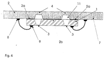
- the mounting body 7 can also be in one piece contain the element designated in FIGS. 1 to 3 with carrier substrate 2, as well is shown in Fig. 4.
- the chip 1 is then not in this case single body but functional area 2a and 2b in connection.
- the mounting body can also be made in one piece with the carrier substrate 2 be trained.
- one sensor element can be implemented in each case is completely seamless. This can be realized if, for example, a Ceramic part, which represents the wall of a pressure vessel, has a location that corresponds to the carrier substrate described so far. In such a case, the swell areas, for example by grinding or by pouring or possibly Generate sintering processes appropriately.
- a disadvantage of these embodiments however, that the connection of carrier substrate 2 and chip 1 is no longer by full-wafer connection techniques can be done.
- the Sandwich arrangement according to the invention for example made of chip and carrier substrate can be viewed as a micromechanical parallelogram structure.
- An embodiment of the sensor arrangement for measuring force can be non-ideal force coupling, which in practice, for example, due to Manufacturing tolerances or thermal changes in the Overall measurement arrangement can occur, a breakdown of force into an intellectual Active component standing vertically on the sandwich surface and into one Interfering components running parallel to the surface occur.
- the Interference component at least partially due to the support of the swell area on Edge of the carrier substrate 2 take place, this interference component then not arrives in the sensor chip 1 more inducing errors.
- the Signal swing for example, with the piezoresistive transducer principle from mechanical Stress of the converter areas depends. It must therefore be taken into account that at According to the rigid design of the carrier substrate, there may be a smaller signal swing in the Chip can result, for example, by a larger gain factor in a signal processing part of the sensor device would have to be compensated.
Landscapes
- Physics & Mathematics (AREA)
- General Physics & Mathematics (AREA)
- Chemical & Material Sciences (AREA)
- Analytical Chemistry (AREA)
- Measuring Fluid Pressure (AREA)
- Pressure Sensors (AREA)
Applications Claiming Priority (2)
| Application Number | Priority Date | Filing Date | Title |
|---|---|---|---|
| DE19810756A DE19810756A1 (de) | 1998-03-12 | 1998-03-12 | Sensoranordnung zur Messung von Druck, Kraft oder Meßgrößen, die sich auf Druck oder Kraft zurückführen lassen, Verfahren zur Herstellung der Sensoranordnung, Sensorelement und Verfahren zur Herstellung des Sensorelements |
| DE19810756 | 1998-03-12 |
Publications (2)
| Publication Number | Publication Date |
|---|---|
| EP0942272A2 true EP0942272A2 (fr) | 1999-09-15 |
| EP0942272A3 EP0942272A3 (fr) | 2001-06-27 |
Family
ID=7860652
Family Applications (1)
| Application Number | Title | Priority Date | Filing Date |
|---|---|---|---|
| EP99103828A Withdrawn EP0942272A3 (fr) | 1998-03-12 | 1999-02-27 | Capteur de mesure de pression, de force ou des grandeurs reliées à une pression ou une force. Procédé de fabrication du capteur. Elément de mesure et procédé de fabrication de l'élément |
Country Status (2)
| Country | Link |
|---|---|
| EP (1) | EP0942272A3 (fr) |
| DE (1) | DE19810756A1 (fr) |
Cited By (3)
| Publication number | Priority date | Publication date | Assignee | Title |
|---|---|---|---|---|
| WO2002033371A3 (fr) * | 2000-10-18 | 2002-08-01 | Endevco Corp | Detecteur de pression |
| WO2012095304A1 (fr) * | 2011-01-12 | 2012-07-19 | Hydac Electronic Gmbh | Dispositif destiné à convertir une force ou une pression en un signal électrique, et procédé de production d'un tel dispositif |
| CN120101984A (zh) * | 2025-05-09 | 2025-06-06 | 杭州电子科技大学 | 一种表面金字塔多级有序压阻型传感器的制备方法及应用 |
Families Citing this family (4)
| Publication number | Priority date | Publication date | Assignee | Title |
|---|---|---|---|---|
| DE10232721A1 (de) | 2002-07-16 | 2004-02-12 | Siemens Ag | Druckgeber mit Drucksensor in mikromechanischer Bauweise |
| DE102010012441B4 (de) * | 2010-03-23 | 2015-06-25 | Bundesrepublik Deutschland, vertreten durch das Bundesministerium für Wirtschaft und Technologie, dieses vertreten durch den Präsidenten der Physikalisch-Technischen Bundesanstalt | Millinewton-Mikrokraftmesser und Verfahren zum Herstellen eines Millinewton-Mikrokraftmessers |
| DE102010022204B4 (de) * | 2010-05-20 | 2016-03-31 | Epcos Ag | Elektrisches Bauelement mit flacher Bauform und Herstellungsverfahren |
| CN113125054B (zh) * | 2020-01-16 | 2023-03-28 | 深圳第三代半导体研究院 | 一种柔性压力传感器及其制造方法 |
Family Cites Families (7)
| Publication number | Priority date | Publication date | Assignee | Title |
|---|---|---|---|---|
| GB1586968A (en) * | 1977-10-10 | 1981-03-25 | Emi Ltd | Pressure transducer |
| US4236137A (en) * | 1979-03-19 | 1980-11-25 | Kulite Semiconductor Products, Inc. | Semiconductor transducers employing flexure frames |
| DE3702412A1 (de) * | 1987-01-28 | 1988-08-18 | Philips Patentverwaltung | Druckaufnehmer mit einem siliziumkoerper |
| JPH0810170B2 (ja) * | 1987-03-06 | 1996-01-31 | 株式会社日立製作所 | 半導体絶対圧力センサの製造方法 |
| DD285831A5 (de) * | 1989-07-11 | 1991-01-03 | Veb Geraete- Und Regler-Werke Teltow,Betrieb Des Veb Kombinat,Dd | Drucksensor fuer kleine druecke |
| JP3300060B2 (ja) * | 1992-10-22 | 2002-07-08 | キヤノン株式会社 | 加速度センサー及びその製造方法 |
| DE19617696C2 (de) * | 1996-05-03 | 1998-04-09 | Thomas Bilger | Mikromechanischer Druck- und Kraftsensor |
-
1998
- 1998-03-12 DE DE19810756A patent/DE19810756A1/de not_active Withdrawn
-
1999
- 1999-02-27 EP EP99103828A patent/EP0942272A3/fr not_active Withdrawn
Cited By (4)
| Publication number | Priority date | Publication date | Assignee | Title |
|---|---|---|---|---|
| WO2002033371A3 (fr) * | 2000-10-18 | 2002-08-01 | Endevco Corp | Detecteur de pression |
| WO2012095304A1 (fr) * | 2011-01-12 | 2012-07-19 | Hydac Electronic Gmbh | Dispositif destiné à convertir une force ou une pression en un signal électrique, et procédé de production d'un tel dispositif |
| US9243964B2 (en) | 2011-01-12 | 2016-01-26 | Hydac Electronic Gmbh | Device for converting a force or a pressure into an electrical signal and method for producing such a device |
| CN120101984A (zh) * | 2025-05-09 | 2025-06-06 | 杭州电子科技大学 | 一种表面金字塔多级有序压阻型传感器的制备方法及应用 |
Also Published As
| Publication number | Publication date |
|---|---|
| DE19810756A1 (de) | 1999-09-23 |
| EP0942272A3 (fr) | 2001-06-27 |
Similar Documents
| Publication | Publication Date | Title |
|---|---|---|
| DE69133193T2 (de) | Verfahren zur Herstellung eines kapazitiven Detektors mit drei Substraten, sich umgebenden Regionen und einem Arbeitskörper ( Kraft, Beschleunigung, magnetisch ) | |
| DE3741941C2 (fr) | ||
| DE102004006201B4 (de) | Drucksensor mit Siliziumchip auf einer Stahlmembran | |
| DE68902534T2 (de) | Kapazitiver Beschleunigungsmesser und Verfahren zu seiner Herstellung. | |
| EP1440322B1 (fr) | Microcapteur | |
| EP2691754B1 (fr) | Capteur de pression différentielle ayant une capsule résistant à la pression | |
| DE69424557T2 (de) | Druckwandler mit aufgehangter membran | |
| EP0623824B1 (fr) | Accéléromètre micro-usine et procédé pour sa fabrication | |
| DE69214940T2 (de) | Drucksensor mit träger mit hohem elastizitätsmodul | |
| DE69211504T2 (de) | Halbleiter-Druckwandler mit zwei Membranen | |
| EP1305585B1 (fr) | Capteur de pression capacitif | |
| DE2709945A1 (de) | Kapazitiver druckwandler und verfahren zu dessen herstellung | |
| EP1382952A1 (fr) | Capteur de pression micromécanique avec le transducteur sur le diaphragme de séparation de la boíte | |
| DE69410061T3 (de) | Flüssigkeitsmessvorrichtung | |
| DE19539178B4 (de) | Halbleiterbeschleunigungssensor und Verfahren zu seiner Herstellung | |
| DE69212507T2 (de) | Piezoresistiver Druckwandler mit leitender, elastomerer Abdichtung | |
| EP0942272A2 (fr) | Capteur de mesure de pression, de force ou des grandeurs reliées à une pression ou une force. Procédé de fabrication du capteur. Elément de mesure et procédé de fabrication de l'élément | |
| WO2019016320A1 (fr) | Système de détection de pression et procédé de fabrication dudit système | |
| EP1516167A1 (fr) | Detecteur et son procede de production | |
| DE10035564B4 (de) | Mikromechanisches Gehäuse | |
| DE102017109971A1 (de) | Drucksensor | |
| WO2014154394A1 (fr) | Corps fritté comprenant plusieurs matériaux et appareil de mesure de pression comprenant un corps fritté de ce type | |
| DE102018119943A1 (de) | Drucksensor | |
| DE102021204645A1 (de) | Verfahren zur Herstellung eines mikroelektromechanischen Sensors aus einem MEMS-Element und einem ASIC-Element und mikroelektromechanischer Sensor | |
| WO2026057304A1 (fr) | Capteur de pression capacitif ayant une structure de détection autoportante |
Legal Events
| Date | Code | Title | Description |
|---|---|---|---|
| PUAI | Public reference made under article 153(3) epc to a published international application that has entered the european phase |
Free format text: ORIGINAL CODE: 0009012 |
|
| 17P | Request for examination filed |
Effective date: 19990227 |
|
| AK | Designated contracting states |
Kind code of ref document: A2 Designated state(s): DE FR GB IT |
|
| AX | Request for extension of the european patent |
Free format text: AL;LT;LV;MK;RO;SI |
|
| PUAL | Search report despatched |
Free format text: ORIGINAL CODE: 0009013 |
|
| AK | Designated contracting states |
Kind code of ref document: A3 Designated state(s): AT BE CH CY DE DK ES FI FR GB GR IE IT LI LU MC NL PT SE |
|
| AX | Request for extension of the european patent |
Free format text: AL;LT;LV;MK;RO;SI |
|
| AKX | Designation fees paid |
Free format text: DE FR GB IT |
|
| RAP1 | Party data changed (applicant data changed or rights of an application transferred) |
Owner name: FRAUNHOFER-GESELLSCHAFT ZUR FOERDERUNG DERANGEWAND |
|
| STAA | Information on the status of an ep patent application or granted ep patent |
Free format text: STATUS: THE APPLICATION IS DEEMED TO BE WITHDRAWN |
|
| 18D | Application deemed to be withdrawn |
Effective date: 20050830 |