EP0942392A2 - Chipkarte - Google Patents
Chipkarte Download PDFInfo
- Publication number
- EP0942392A2 EP0942392A2 EP99103979A EP99103979A EP0942392A2 EP 0942392 A2 EP0942392 A2 EP 0942392A2 EP 99103979 A EP99103979 A EP 99103979A EP 99103979 A EP99103979 A EP 99103979A EP 0942392 A2 EP0942392 A2 EP 0942392A2
- Authority
- EP
- European Patent Office
- Prior art keywords
- card
- semiconductor device
- type semiconductor
- semiconductor element
- leads
- Prior art date
- Legal status (The legal status is an assumption and is not a legal conclusion. Google has not performed a legal analysis and makes no representation as to the accuracy of the status listed.)
- Withdrawn
Links
Images

Classifications
-
- G—PHYSICS
- G06—COMPUTING OR CALCULATING; COUNTING
- G06K—GRAPHICAL DATA READING; PRESENTATION OF DATA; RECORD CARRIERS; HANDLING RECORD CARRIERS
- G06K19/00—Record carriers for use with machines and with at least a part designed to carry digital markings
- G06K19/06—Record carriers for use with machines and with at least a part designed to carry digital markings characterised by the kind of the digital marking, e.g. shape, nature, code
- G06K19/067—Record carriers with conductive marks, printed circuits or semiconductor circuit elements, e.g. credit or identity cards also with resonating or responding marks without active components
- G06K19/07—Record carriers with conductive marks, printed circuits or semiconductor circuit elements, e.g. credit or identity cards also with resonating or responding marks without active components with integrated circuit chips
- G06K19/077—Constructional details, e.g. mounting of circuits in the carrier
- G06K19/0772—Physical layout of the record carrier
- G06K19/07728—Physical layout of the record carrier the record carrier comprising means for protection against impact or bending, e.g. protective shells or stress-absorbing layers around the integrated circuit
-
- G—PHYSICS
- G06—COMPUTING OR CALCULATING; COUNTING
- G06K—GRAPHICAL DATA READING; PRESENTATION OF DATA; RECORD CARRIERS; HANDLING RECORD CARRIERS
- G06K19/00—Record carriers for use with machines and with at least a part designed to carry digital markings
- G06K19/06—Record carriers for use with machines and with at least a part designed to carry digital markings characterised by the kind of the digital marking, e.g. shape, nature, code
- G06K19/067—Record carriers with conductive marks, printed circuits or semiconductor circuit elements, e.g. credit or identity cards also with resonating or responding marks without active components
- G06K19/07—Record carriers with conductive marks, printed circuits or semiconductor circuit elements, e.g. credit or identity cards also with resonating or responding marks without active components with integrated circuit chips
- G06K19/077—Constructional details, e.g. mounting of circuits in the carrier
- G06K19/07745—Mounting details of integrated circuit chips
-
- H—ELECTRICITY
- H10—SEMICONDUCTOR DEVICES; ELECTRIC SOLID-STATE DEVICES NOT OTHERWISE PROVIDED FOR
- H10W—GENERIC PACKAGES, INTERCONNECTIONS, CONNECTORS OR OTHER CONSTRUCTIONAL DETAILS OF DEVICES COVERED BY CLASS H10
- H10W72/00—Interconnections or connectors in packages
- H10W72/50—Bond wires
- H10W72/531—Shapes of wire connectors
- H10W72/536—Shapes of wire connectors the connected ends being ball-shaped
-
- H—ELECTRICITY
- H10—SEMICONDUCTOR DEVICES; ELECTRIC SOLID-STATE DEVICES NOT OTHERWISE PROVIDED FOR
- H10W—GENERIC PACKAGES, INTERCONNECTIONS, CONNECTORS OR OTHER CONSTRUCTIONAL DETAILS OF DEVICES COVERED BY CLASS H10
- H10W72/00—Interconnections or connectors in packages
- H10W72/50—Bond wires
- H10W72/531—Shapes of wire connectors
- H10W72/5363—Shapes of wire connectors the connected ends being wedge-shaped
-
- H—ELECTRICITY
- H10—SEMICONDUCTOR DEVICES; ELECTRIC SOLID-STATE DEVICES NOT OTHERWISE PROVIDED FOR
- H10W—GENERIC PACKAGES, INTERCONNECTIONS, CONNECTORS OR OTHER CONSTRUCTIONAL DETAILS OF DEVICES COVERED BY CLASS H10
- H10W72/00—Interconnections or connectors in packages
- H10W72/50—Bond wires
- H10W72/551—Materials of bond wires
- H10W72/552—Materials of bond wires comprising metals or metalloids, e.g. silver
- H10W72/5522—Materials of bond wires comprising metals or metalloids, e.g. silver comprising gold [Au]
-
- H—ELECTRICITY
- H10—SEMICONDUCTOR DEVICES; ELECTRIC SOLID-STATE DEVICES NOT OTHERWISE PROVIDED FOR
- H10W—GENERIC PACKAGES, INTERCONNECTIONS, CONNECTORS OR OTHER CONSTRUCTIONAL DETAILS OF DEVICES COVERED BY CLASS H10
- H10W74/00—Encapsulations, e.g. protective coatings
Definitions
- the present invention relates to a card-type semiconductor device such as an IC card.
- Card-type semiconductor devices with a semiconductor chip built in, called IC card, are being developed actively these years.
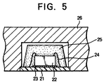
- Reference numeral 21 denotes a wiring substrate, which has a desired wiring layer formed on one side (the upper face in the drawing) of an insulating substrate and a wiring layer to be an external connection terminal on the other side (the lower face in the drawing). Both wiring layers are electrically connected through conductive holes (not shown).
- a semiconductor chip 22 is mounted onto the upper face of the wiring substrate 21 with an insulating adhesive agent (mounting agent) 23, and its electrode pads are connected to the wiring layer of the wiring substrate 21 by bonding wires 24 such as gold wires.
- a mold resin layer 25 of epoxy resin layer or the like is formed on the exterior of the wire-bonded portion.
- the resin-molded chip-mounted section is fitted into a recess of an exterior sheet 26 made of polyvinyl chloride resin, polyester resin or the like, and the wiring layer on the lower face of the wiring substrate 21 is exposed as external connection terminal.
- Such a conventional card-type semiconductor device could not be fabricated to have a satisfactory small thinness because the semiconductor chip 22 has a large thickness of 350 to 450 ⁇ m and defines an overall thickness of the device.
- the IC card is required to have a strength enough to resist against an impact, bending, twisting, etc. due to an external force. But the card-type semiconductor device, which has the above-described thick semiconductor chip 22 mounted, could not meet the requirement in terms of a bending strength and the like.
- the present invention was achieved to remedy the problems described above. And it is an object of the invention to provide a card-type semiconductor device, which is thin with a sufficient strength against bending, twisting and the like and suitable as an IC card.
- a first aspect of the present invention is a card-type semiconductor device, which comprises;
- a second aspect of the present invention is a card-type semiconductor device, which comprises a semiconductor element and an enclosure portion made of an insulating resin for fully covering the periphery of the semiconductor element without remaining any gap;
- the film insulating substrate can be an insulating resin film such as a polyimide resin film (trade name: UPILEX manufactured by Ube Industries, Ltd.).
- the film preferably has a thickness of 75 to 125 ⁇ m.
- the device hole formed in the insulating resin film has such a size and a plane shape to correspond with those of the semiconductor element to be described afterward, so that the semiconductor element is embedded with a sufficient allowance around it.
- the wiring layer formed on at least one main face of the film insulating substrate and the group of leads whose one end connected to the wiring layer are formed of Cu, a Cu-based alloy or the like by deposition patterning of such metal on the insulating substrate or photo-etching of a Cu foil or the like, which is directly laminated on the insulating substrate or with an adhesive agent layer such as an epoxy-based layer or the like between them.
- the end (leading end) of the group of leads protruded into the device hole is bonded (inner lead bonding) to the electrode pads, made of aluminum or the like, of the semiconductor element by heating and pressing. It is desirable that the leading ends of the leads are coated with a gold, tin or solder layer by plating or the like in order to improve their bonding strength.
- the electrode pads of the semiconductor element may be bonded to the leads through the gold bumps formed on the electrode pads. The bonding strength can be further improved by bonding the leads, which are plated with gold, tin or the like, to the gold bumps formed on the electrode pads.
- the leading ends of the leads have a width smaller than that of the electrode pads or that of the gold bumps formed on the electrode pads.
- the invention can use an insulating resin film having flexibility, such as a polyester resin film, as the exterior layer.
- This insulating resin film is laminated on both faces of the film substrate (wiring film), on which the above-described wiring layer or the like is formed, by thermal fusion bonding for example.
- the film is not limited to have a particular thickness but preferably has a thickness of about 50 ⁇ m (25 to 75 ⁇ m) so to protect as an enclosure its inside and also to contribute in making the device thinner as a whole.
- the semiconductor element is preferably a thin semiconductor element having each side of 3 to 6 mm and a thickness of 30 to 70 ⁇ m which is thinner than the film insulating substrate so that it can be fully embedded in the device hole of the above-described film insulating substrate.
- the card-type semiconductor device having a bending radius to allow repeated bending (hereinafter referred to as the bending radius) of 15 to 40 mm can be realized.
- the card-type semiconductor device such as the IC card
- Strength against bending which is required for the card-type semiconductor device such as the IC card is not standardized yet. But it is expected that the card-type semiconductor device has such a very high bending strength corresponding to that of the conventional Japanese magnetic telephone card that its appearance and function are not affected even after repeatedly applying strong bending (e.g., a bending radius of about 166 mm on the long side) for about 1000 times.
- strong bending e.g., a bending radius of about 166 mm on the long side
- the semiconductor element having a thickness of 30 to 70 ⁇ m has a bending radius of about 17 to 33 mm though it is slightly variable depending on a grinding direction and a very high bending strength as large as 7 times or more as compared with a conventionally used semiconductor element having a thickness of 350 to 450 ⁇ m (a bending radius of about 200 mm).
- a necessary and sufficient bending strength for the IC card can be realized for the first time by using the semiconductor element having a thickness of 30 to 70 ⁇ m.
- the semiconductor element having a thickness of less than 30 ⁇ m is not processed with ease, the yield of its manufacture is not good, and its strength against bending and the like is low.
- the above-described thin semiconductor element is preferably not fixed to the exterior layer laminated on the upper and lower faces of the wiring film.
- the enclosure portion made of an insulating resin is also required to have the same or smaller bending radius as the above-described semiconductor element.
- the polyimide resin film used as the film insulating substrate and the polyester resin film used as the exterior layer have good flexibility, a much smaller bending radius than 15 mm and a mechanical strength sufficient to protect the semiconductor element from an external pressure. Since such films are used to configure the enclosure portion, the card-type semiconductor device having a bending radius of 15 to 40 mm can be obtained.
- the card-type semiconductor device according to the invention can be made to have a very small thickness of 200 ⁇ m or below as a whole because the very thin semiconductor element which is thinner than the film insulating substrate is fully embedded in the device hole of the insulating substrate. Besides its strength against bending, twisting, local striking/pushing and the like is highly improved as compared with a conventional card-type semiconductor device.
- the semiconductor device according to the invention When the semiconductor device according to the invention is used as the IC card, it can fully meet a very high bending strength required.
- ILB inner lead bonding
- bonding work can be made efficiently without paying attention to an edge touch of the inner leads to the semiconductor element.
- productivity is high, and a yield is improved.
- Fig. 1 is a diagram showing a cross section of main portions of a first embodiment of a card-type semiconductor device according to the invention.
- reference numeral 1 denotes an insulating resin film (e.g., polyimide resin film) with a thickness of 75 to 125 ⁇ m, which has a device hole 1a at the center.
- a wiring layer 2 is formed on one face of the insulating resin film 1 by, for example, photo-etching a copper foil which is adhered to the film with an adhesive layer (not shown) between them. Ends of the wiring layer 2 are protruded into the device hole 1a to form inner leads 3. Leading tips of the inner leads 3 are plated with gold or the like (not shown) in order to facilitate the connection with the electrode pads.
- a semiconductor chip 4 having each side of 3 to 6 mm and a thickness smaller than that of the insulating resin film 1 is mounted on the wiring film as follows. Specifically, the semiconductor chip 4, whose each side is smaller than the corresponding side of the device hole 1a and thickness is 30 to 70 ⁇ m, is embedded with a face up into the device hole 1a, and each electrode pad (not shown) of the semiconductor chip 4 is bonded to the inner leads 3 by ILB(inner lead bonding).
- This card-type semiconductor device has a coil-shaped antenna made of wiring for transmitting/receiving data to make reading and writing of data with an external processing device by radio (contactless). This portion is omitted from being shown in the drawing.
- the card-type semiconductor device of the first embodiment configured as described above has the thin semiconductor chip 4 with a thickness of 30 to 70 ⁇ m, which is thinner than the insulating resin film 1, fully embedded into the device hole 1a of the insulating resin film 1.
- the polyester resin film 5, which has a thickness of about 50 ⁇ m and flexibility, is integrally laminated on the upper and lower faces of the insulating resin film. Therefore, this card-type semiconductor device has a very small total thickness and can fulfill the requirement for a thickness of the IC card with sufficient allowance. It also has a small bending radius of 15 to 40 mm allowing repeated bending and a high strength against bending, twisting, striking/pushing and the like.
- the thin semiconductor chip 4 Since the thin semiconductor chip 4 is mounted in a free independent state within the device hole 1a without being fixed to the polyester resin film 5, which is formed on the upper and lower faces of the insulating resin film, a bending strength of the connected portion between the semiconductor chip 4 and the inner leads 3 is high, so that a connection failure occurs very seldom.
- the semiconductor chip 4 can be mounted simply by connecting it to the inner leads 3 and fitting into the device hole 1a and does not need its positioning.
- the semiconductor chip 4 of the first embodiment is thinner than the insulating resin film 1, the ILB processing of the semiconductor chip 4 can be effected efficiently.
- the ILB process conventionally adopts a method by which the wiring film is set at a position higher than the semiconductor chip and the inner leads extended from the high position is connected to the electrode pads of the semiconductor chip in order to prevent the inner leads from making an edge touch to the semiconductor chip.
- the wiring film and the semiconductor chip 4 are placed on one and same stage 6, and thermosonic bonding by a bonding tool 7 can be effected efficiently by applying ultrasonic waves without caring about the edge touch of the inner leads 3 to the semiconductor chip 4 as shown in Fig. 2.
- the semiconductor device obtained has a higher bending strength. Furthermore, in the ILB performed on the same stage 6, the back face (the face opposite from the electrode-formed face) of the semiconductor chip 4 and the back face of the wiring film are arranged at the same height, so that fusion bonding of the polyester resin film 5 to both faces of the wiring film by heating is made with ease.
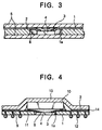
- Fig. 3 is a diagram showing a cross section of main components of a second embodiment of the card-type semiconductor device according to the invention.
- a sealing resin layer 8 is formed by potting on the electrode pad-formed face of the semiconductor chip 4 embedded in the device hole 1a and the exterior of the bonded portion between the electrode pads and the inner leads 3.
- a material for the sealing resin layer 8 may be epoxy resin, silicone resin or the like. Especially, when the silicone resin is used, water-vapor resistance of the semiconductor chip 4 is improved, and the semiconductor device obtained has a smaller bending radius than one obtained using the epoxy resin.
- the same reference numerals as in Fig. 1 are allotted and their description is not repeated.
- the thin (a thickness of 30 to 70 ⁇ m) semiconductor chip 4 is fully embedded in the device hole 1a of an insulating resin film 1, and a thin, flexible polyester resin film 5 is integrally laminated on upper and lower faces of the insulting resin film 1 in the same way as in the first embodiment. Therefore, the semiconductor device has a very small overall thickness and can meet the requirements for the IC card. Besides, the semiconductor device has a small bending radius of 15 to 40 mm and a high strength against bending, twisting, striking/pushing and the like.
- Moisture resistance of the semiconductor chip 4 is improved because the resin-sealing layer 8 is formed on the exterior of the bonded portion and the like of the semiconductor chip 4. Since the sealing resin layer 8 is made of the silicone resin, good flexural properties (smallness of a bending radius) of the semiconductor chip 4 and enclosure portions (the insulating resin film 1 and the polyester resin film 5) are not deteriorated.
- the thin semiconductor device which has a semiconductor chip having each side of 3 to 6 mm long and a thickness of 30 to 70 ⁇ m smaller than that of an ordinary insulating resin film mounted in the device hole, may have another semiconductor chip which is mounted to cover at least a part of the opening of the device hole as shown in Fig. 4.
- the wiring layer 2 is formed by photo-etching a copper foil on one main face of the insulating resin film (e.g., polyimide resin film) having a thickness of 75 to 125 ⁇ m and a device hole 1a, and holes 9 are also formed to electrically connect the wiring layer 2 to the opposite face.
- the ends of the wiring layer 2 are protruded as the inner leads 3 into the device hole 1a.
- the first thin semiconductor chip 4 which has each side length smaller than the corresponding side of the device hole 1a and a thickness of 30 to 70 ⁇ m which is smaller than that of the insulating resin film 1, is embedded with a face up within the device hole 1a of the wiring film, and its electrode pads are bonded to the inner leads 3 of the wiring film by thermosonic bonding.
- a second semiconductor chip 10 is mounted above the first thin semiconductor chip 4 connected as described above with an appropriate space held between them.
- the second semiconductor chip 10 which has a thickness larger than that of the insulating resin film 1 and each side larger than the corresponding side of the device hole 1a, is disposed with a face down to cover the opening of the device hole 1a, and the electrode pads and the wiring layer 2 on the upper face of the wiring film are flip-chip bonded through solder bumps 11 or gold bumps.
- the sealing resin layer 8 of epoxy resin or the like is formed in the space between the upper and lower semiconductor chips mounted as described above.
- Solder balls 12 as external connection terminals are formed on the lower face of the wiring film and electrically connected to the wiring layer 2 on the upper face of the wiring film through the via holes.
- a cover plate 13 having a shape retaining property is adhered to the wiring layer 2 on the upper face of the film and the upper semiconductor chip 10 with an adhesive layer 14.
- the semiconductor device configured as described above the first and second semiconductor chips 4, 10 which are overlaid vertically are mounted, so that the increase of pads for connecting the bumps and the decrease of the pad pitch due to the increase of chips can be complied with, and the semiconductor device obtained having the semiconductor chips mounted at a high density is obtained.
- the semiconductor device as a whole can be kept to have the same thickness as a semiconductor device which has only one ordinary semiconductor chip mounted. Furthermore, this semiconductor device is suitable for high-frequency equipment because a wiring length is made short.
- the card-type semiconductor device according to the invention can be made to have a very small thickness as a whole because the very thin semiconductor element, which is thinner than the film insulating substrate, is fully embedded into the device hole of the insulating substrate. Besides, it has a sufficient strength against bending, twisting, local striking/pushing and the like and is suitable as the IC card.
- the semiconductor element can be mounted in the semiconductor device with good workability.
Landscapes
- Engineering & Computer Science (AREA)
- Computer Hardware Design (AREA)
- Microelectronics & Electronic Packaging (AREA)
- Physics & Mathematics (AREA)
- General Physics & Mathematics (AREA)
- Theoretical Computer Science (AREA)
- Credit Cards Or The Like (AREA)
- Structures Or Materials For Encapsulating Or Coating Semiconductor Devices Or Solid State Devices (AREA)
Applications Claiming Priority (2)
| Application Number | Priority Date | Filing Date | Title |
|---|---|---|---|
| JP6313598 | 1998-03-13 | ||
| JP6313598 | 1998-03-13 |
Publications (2)
| Publication Number | Publication Date |
|---|---|
| EP0942392A2 true EP0942392A2 (de) | 1999-09-15 |
| EP0942392A3 EP0942392A3 (de) | 2000-10-18 |
Family
ID=13220536
Family Applications (1)
| Application Number | Title | Priority Date | Filing Date |
|---|---|---|---|
| EP99103979A Withdrawn EP0942392A3 (de) | 1998-03-13 | 1999-03-10 | Chipkarte |
Country Status (2)
| Country | Link |
|---|---|
| US (1) | US6208019B1 (de) |
| EP (1) | EP0942392A3 (de) |
Families Citing this family (25)
| Publication number | Priority date | Publication date | Assignee | Title |
|---|---|---|---|---|
| US6268237B1 (en) * | 1995-04-03 | 2001-07-31 | Aptek Industries, Inc. | Stress-free silicon wafer and a die or chip made therefrom and method |
| US6412702B1 (en) * | 1999-01-25 | 2002-07-02 | Mitsumi Electric Co., Ltd. | Non-contact IC card having an antenna coil formed by a plating method |
| FR2793330B1 (fr) * | 1999-05-06 | 2001-08-10 | Oberthur Card Systems Sas | Procede de montage d'un microcircuit dans une cavite d'une carte formant support et carte ainsi obtenue |
| FR2795846B1 (fr) * | 1999-07-01 | 2001-08-31 | Schlumberger Systems & Service | PROCEDE DE FABRICATION DE CARTES LAMINEES MUNIES D'UNE COUCHE INTERMEDIAIRES DE petg |
| US6396138B1 (en) * | 2000-02-15 | 2002-05-28 | International Rectifier Corporation | Chip array with two-sided cooling |
| US6462273B1 (en) * | 2001-03-16 | 2002-10-08 | Micron Technology, Inc. | Semiconductor card and method of fabrication |
| JP2003007976A (ja) * | 2001-06-25 | 2003-01-10 | Mitsubishi Electric Corp | 半導体装置及びモジュール装置 |
| US6548759B1 (en) * | 2001-06-28 | 2003-04-15 | Amkor Technology, Inc. | Pre-drilled image sensor package |
| US6730536B1 (en) | 2001-06-28 | 2004-05-04 | Amkor Technology, Inc. | Pre-drilled image sensor package fabrication method |
| US6486545B1 (en) | 2001-07-26 | 2002-11-26 | Amkor Technology, Inc. | Pre-drilled ball grid array package |
| US20050196604A1 (en) * | 2004-03-05 | 2005-09-08 | Unifoil Corporation | Metallization process and product produced thereby |
| US7459376B2 (en) * | 2005-02-04 | 2008-12-02 | Infineon Technologies Ag | Dissociated fabrication of packages and chips of integrated circuits |
| US7685706B2 (en) * | 2005-07-08 | 2010-03-30 | Semiconductor Energy Laboratory Co., Ltd | Method of manufacturing a semiconductor device |
| DE102005047106B4 (de) * | 2005-09-30 | 2009-07-23 | Infineon Technologies Ag | Leistungshalbleitermodul und Verfahren zur Herstellung |
| JP5346497B2 (ja) * | 2007-06-12 | 2013-11-20 | 株式会社半導体エネルギー研究所 | 半導体装置 |
| US7707706B2 (en) * | 2007-06-29 | 2010-05-04 | Ruhlamat Gmbh | Method and arrangement for producing a smart card |
| US8690064B2 (en) * | 2009-04-30 | 2014-04-08 | Abnote Usa, Inc. | Transaction card assembly and methods of manufacture |
| US8803185B2 (en) * | 2012-02-21 | 2014-08-12 | Peiching Ling | Light emitting diode package and method of fabricating the same |
| US20140374151A1 (en) * | 2013-06-24 | 2014-12-25 | Jia Lin Yap | Wire bonding method for flexible substrates |
| EP2840375A1 (de) * | 2013-08-19 | 2015-02-25 | Sensirion AG | Vorrichtung mit einer mikro- oder nanoskaligen Struktur |
| EP3367082A1 (de) | 2013-11-06 | 2018-08-29 | Invensense, Inc. | Drucksensor |
| EP2871455B1 (de) | 2013-11-06 | 2020-03-04 | Invensense, Inc. | Drucksensor |
| EP3614115B1 (de) | 2015-04-02 | 2024-09-11 | InvenSense, Inc. | Drucksensor |
| US11225409B2 (en) | 2018-09-17 | 2022-01-18 | Invensense, Inc. | Sensor with integrated heater |
| WO2020236661A1 (en) | 2019-05-17 | 2020-11-26 | Invensense, Inc. | A pressure sensor with improve hermeticity |
Family Cites Families (41)
| Publication number | Priority date | Publication date | Assignee | Title |
|---|---|---|---|---|
| US3702464A (en) * | 1971-05-04 | 1972-11-07 | Ibm | Information card |
| DE3019207A1 (de) * | 1980-05-20 | 1981-11-26 | GAO Gesellschaft für Automation und Organisation mbH, 8000 München | Traegerelement fuer einen ic-chip |
| FR2486685B1 (fr) * | 1980-07-09 | 1985-10-31 | Labo Electronique Physique | Carte de paiement electronique et procede de realisation |
| DE3051195C2 (de) * | 1980-08-05 | 1997-08-28 | Gao Ges Automation Org | Trägerelement zum Einbau in Ausweiskarten |
| DE3123198C2 (de) * | 1980-12-08 | 1993-10-07 | Gao Ges Automation Org | Trägerelemente für einen IC-Baustein |
| US4409471A (en) * | 1981-12-17 | 1983-10-11 | Seiichiro Aigo | Information card |
| US4447716A (en) * | 1982-03-01 | 1984-05-08 | Seiichiro Aigo | Information card |
| FR2527036A1 (fr) * | 1982-05-14 | 1983-11-18 | Radiotechnique Compelec | Procede pour connecter un semiconducteur a des elements d'un support, notamment d'une carte portative |
| DE3235650A1 (de) * | 1982-09-27 | 1984-03-29 | Philips Patentverwaltung Gmbh, 2000 Hamburg | Informationskarte und verfahren zu ihrer herstellung |
| DE3248385A1 (de) * | 1982-12-28 | 1984-06-28 | GAO Gesellschaft für Automation und Organisation mbH, 8000 München | Ausweiskarte mit integriertem schaltkreis |
| DE3338597A1 (de) * | 1983-10-24 | 1985-05-02 | GAO Gesellschaft für Automation und Organisation mbH, 8000 München | Datentraeger mit integriertem schaltkreis und verfahren zur herstellung desselben |
| FR2581480A1 (fr) * | 1985-04-10 | 1986-11-07 | Ebauches Electroniques Sa | Unite electronique notamment pour carte a microcircuits et carte comprenant une telle unite |
| JPH074995B2 (ja) * | 1986-05-20 | 1995-01-25 | 株式会社東芝 | Icカ−ド及びその製造方法 |
| KR940003375B1 (ko) * | 1986-05-21 | 1994-04-21 | 가부시끼가이샤 히다찌세이사꾸쇼 | 반도체 장치 및 그 제조 방법 |
| FR2599893B1 (fr) * | 1986-05-23 | 1996-08-02 | Ricoh Kk | Procede de montage d'un module electronique sur un substrat et carte a circuit integre |
| JPS6394645A (ja) * | 1986-10-08 | 1988-04-25 | Mitsubishi Electric Corp | 電子装置 |
| US5067008A (en) * | 1989-08-11 | 1991-11-19 | Hitachi Maxell, Ltd. | Ic package and ic card incorporating the same thereinto |
| DE69020077T2 (de) * | 1989-09-09 | 1995-11-09 | Mitsubishi Electric Corp | Integrierte Schaltungskarte. |
| US5227338A (en) * | 1990-04-30 | 1993-07-13 | International Business Machines Corporation | Three-dimensional memory card structure with internal direct chip attachment |
| FR2662000A1 (fr) * | 1990-05-11 | 1991-11-15 | Philips Composants | Carte a microcircuit. |
| JP2560895B2 (ja) * | 1990-07-25 | 1996-12-04 | 三菱電機株式会社 | Icカードの製造方法およびicカード |
| US5250600A (en) * | 1992-05-28 | 1993-10-05 | Johnson Matthey Inc. | Low temperature flexible die attach adhesive and articles using same |
| FR2691563B1 (fr) * | 1992-05-19 | 1996-05-31 | Francois Droz | Carte comprenant au moins un element electronique et procede de fabrication d'une telle carte. |
| US5324687A (en) * | 1992-10-16 | 1994-06-28 | General Electric Company | Method for thinning of integrated circuit chips for lightweight packaged electronic systems |
| KR950704758A (ko) * | 1993-10-18 | 1995-11-20 | 가나미야지 준 | IC 모듈과 그것을 사용한 데이터 커리어(Ic module using it on data carrier) |
| US5581445A (en) * | 1994-02-14 | 1996-12-03 | Us3, Inc. | Plastic integrated circuit card with reinforcement structure for protecting integrated circuit module |
| US5480842A (en) * | 1994-04-11 | 1996-01-02 | At&T Corp. | Method for fabricating thin, strong, and flexible die for smart cards |
| US5917705A (en) * | 1994-04-27 | 1999-06-29 | Siemens Aktiengesellschaft | Chip card |
| DE4416697A1 (de) * | 1994-05-11 | 1995-11-16 | Giesecke & Devrient Gmbh | Datenträger mit integriertem Schaltkreis |
| JP3186925B2 (ja) * | 1994-08-04 | 2001-07-11 | シャープ株式会社 | パネルの実装構造並びに集積回路搭載テープおよびその製造方法 |
| DE69621983T2 (de) * | 1995-04-07 | 2002-11-21 | Shinko Electric Industries Co., Ltd. | Struktur und Verfahren zur Montage eines Halbleiterchips |
| US5773775A (en) * | 1995-05-17 | 1998-06-30 | Alps Electric Co., Ltd. | Pressure actuated circuit breaker with frangible printed circuit board |
| JPH08310172A (ja) * | 1995-05-23 | 1996-11-26 | Hitachi Ltd | 半導体装置 |
| DE19528730A1 (de) * | 1995-08-04 | 1997-02-06 | Giesecke & Devrient Gmbh | Verfahren zur Herstellung eines Datenträgers |
| JP2987101B2 (ja) * | 1996-04-15 | 1999-12-06 | 株式会社ニッシン | 半導体装置の接続方法並びに半導体装置の接続器 |
| DE19617055C1 (de) * | 1996-04-29 | 1997-06-26 | Semikron Elektronik Gmbh | Halbleiterleistungsmodul hoher Packungsdichte in Mehrschichtbauweise |
| JPH09327990A (ja) * | 1996-06-11 | 1997-12-22 | Toshiba Corp | カード型記憶装置 |
| US5773884A (en) * | 1996-06-27 | 1998-06-30 | International Business Machines Corporation | Electronic package with thermally conductive support member having a thin circuitized substrate and semiconductor device bonded thereto |
| US5786988A (en) * | 1996-07-02 | 1998-07-28 | Sandisk Corporation | Integrated circuit chips made bendable by forming indentations in their back surfaces flexible packages thereof and methods of manufacture |
| US6027958A (en) * | 1996-07-11 | 2000-02-22 | Kopin Corporation | Transferred flexible integrated circuit |
| JP3322575B2 (ja) * | 1996-07-31 | 2002-09-09 | 太陽誘電株式会社 | ハイブリッドモジュールとその製造方法 |
-
1999
- 1999-03-10 US US09/265,924 patent/US6208019B1/en not_active Expired - Lifetime
- 1999-03-10 EP EP99103979A patent/EP0942392A3/de not_active Withdrawn
Also Published As
| Publication number | Publication date |
|---|---|
| US6208019B1 (en) | 2001-03-27 |
| EP0942392A3 (de) | 2000-10-18 |
Similar Documents
| Publication | Publication Date | Title |
|---|---|---|
| US6208019B1 (en) | Ultra-thin card-type semiconductor device having an embredded semiconductor element in a space provided therein | |
| US6515356B1 (en) | Semiconductor package and method for fabricating the same | |
| US6344683B1 (en) | Stacked semiconductor package with flexible tape | |
| US6153924A (en) | Multilayered lead frame for semiconductor package | |
| JP3032964B2 (ja) | ボールグリッドアレイ半導体のパッケージ及び製造方法 | |
| EP0500690B1 (de) | Mehrlagenleiterrahmen für integrierte schaltungspackungen | |
| US6995448B2 (en) | Semiconductor package including passive elements and method of manufacture | |
| US6982485B1 (en) | Stacking structure for semiconductor chips and a semiconductor package using it | |
| US8991711B2 (en) | Chip card module | |
| JP2001077293A (ja) | 半導体装置 | |
| US20040124516A1 (en) | Circuit device, circuit module, and method for manufacturing circuit device | |
| KR20100010747A (ko) | 반도체 소자 패키지 | |
| CN105938802B (zh) | 树脂密封型半导体装置及其制造方法 | |
| US9728478B2 (en) | Resin-encapsulatd semiconductor device and method of manufacturing the same | |
| KR100610144B1 (ko) | 플립 칩 조립 구조를 가지는 칩-온-보드 패키지의 제조 방법 | |
| JP2000124235A (ja) | 樹脂封止半導体装置 | |
| CN100401487C (zh) | 半导体器件及半导体器件的制造方法 | |
| KR100470144B1 (ko) | 테이프회로기판및이를사용한칩크기의반도체칩패키지 | |
| JPH11330148A (ja) | 半導体装置 | |
| JP3877988B2 (ja) | 半導体装置 | |
| US20030122224A1 (en) | Lead frame with dual thin film coated on inner lead terminal | |
| KR20210060476A (ko) | 휴대용 오브젝트용 전자 모듈을 제조하기 위한 방법 | |
| KR100533762B1 (ko) | 반도체패키지 | |
| US20090026630A1 (en) | Semiconductor device and method for manufacturing same | |
| JPH07326690A (ja) | 半導体装置用パッケージおよび半導体装置 |
Legal Events
| Date | Code | Title | Description |
|---|---|---|---|
| PUAI | Public reference made under article 153(3) epc to a published international application that has entered the european phase |
Free format text: ORIGINAL CODE: 0009012 |
|
| 17P | Request for examination filed |
Effective date: 19990310 |
|
| AK | Designated contracting states |
Kind code of ref document: A2 Designated state(s): DE FR GB |
|
| AX | Request for extension of the european patent |
Free format text: AL;LT;LV;MK;RO;SI |
|
| PUAL | Search report despatched |
Free format text: ORIGINAL CODE: 0009013 |
|
| AK | Designated contracting states |
Kind code of ref document: A3 Designated state(s): AT BE CH CY DE DK ES FI FR GB GR IE IT LI LU MC NL PT SE |
|
| AX | Request for extension of the european patent |
Free format text: AL;LT;LV;MK;RO;SI |
|
| AKX | Designation fees paid |
Free format text: DE FR GB |
|
| 17Q | First examination report despatched |
Effective date: 20021018 |
|
| STAA | Information on the status of an ep patent application or granted ep patent |
Free format text: STATUS: THE APPLICATION IS DEEMED TO BE WITHDRAWN |
|
| 18D | Application deemed to be withdrawn |
Effective date: 20050330 |