EP0942430A1 - Procédé et dispositif de mémoire compatible avec une 1-T SRAM - Google Patents
Procédé et dispositif de mémoire compatible avec une 1-T SRAM Download PDFInfo
- Publication number
- EP0942430A1 EP0942430A1 EP99301728A EP99301728A EP0942430A1 EP 0942430 A1 EP0942430 A1 EP 0942430A1 EP 99301728 A EP99301728 A EP 99301728A EP 99301728 A EP99301728 A EP 99301728A EP 0942430 A1 EP0942430 A1 EP 0942430A1
- Authority
- EP
- European Patent Office
- Prior art keywords
- refresh
- memory
- cells
- access
- external
- Prior art date
- Legal status (The legal status is an assumption and is not a legal conclusion. Google has not performed a legal analysis and makes no representation as to the accuracy of the status listed.)
- Granted
Links
Images

Classifications
-
- G—PHYSICS
- G11—INFORMATION STORAGE
- G11C—STATIC STORES
- G11C11/00—Digital stores characterised by the use of particular electric or magnetic storage elements; Storage elements therefor
- G11C11/21—Digital stores characterised by the use of particular electric or magnetic storage elements; Storage elements therefor using electric elements
- G11C11/34—Digital stores characterised by the use of particular electric or magnetic storage elements; Storage elements therefor using electric elements using semiconductor devices
- G11C11/40—Digital stores characterised by the use of particular electric or magnetic storage elements; Storage elements therefor using electric elements using semiconductor devices using transistors
- G11C11/401—Digital stores characterised by the use of particular electric or magnetic storage elements; Storage elements therefor using electric elements using semiconductor devices using transistors forming cells needing refreshing or charge regeneration, i.e. dynamic cells
- G11C11/406—Management or control of the refreshing or charge-regeneration cycles
- G11C11/40615—Internal triggering or timing of refresh, e.g. hidden refresh, self refresh, pseudo-SRAMs
-
- G—PHYSICS
- G11—INFORMATION STORAGE
- G11C—STATIC STORES
- G11C11/00—Digital stores characterised by the use of particular electric or magnetic storage elements; Storage elements therefor
- G11C11/21—Digital stores characterised by the use of particular electric or magnetic storage elements; Storage elements therefor using electric elements
- G11C11/34—Digital stores characterised by the use of particular electric or magnetic storage elements; Storage elements therefor using electric elements using semiconductor devices
- G11C11/40—Digital stores characterised by the use of particular electric or magnetic storage elements; Storage elements therefor using electric elements using semiconductor devices using transistors
- G11C11/401—Digital stores characterised by the use of particular electric or magnetic storage elements; Storage elements therefor using electric elements using semiconductor devices using transistors forming cells needing refreshing or charge regeneration, i.e. dynamic cells
- G11C11/406—Management or control of the refreshing or charge-regeneration cycles
Definitions
- This invention relates to semiconductor memory.
- it relates to both SRAM and DRAM, and to using DRAM cells for building SRAM compatible memory.
- a conventional DRAM (dynamic random access memory) memory cell consisting of one transistor (“1-T”) and one capacitor is significantly smaller, in terms of chip surface area, and hence less expensive than an SRAM (static random access memory) cell which conventionally consists of 4 to 6 transistors.
- data stored in the DRAM cell requires periodic refresh, which is not required in the SRAM cell.
- Prior art for example "pseudo-SRAM” (see Toshiba Corp. Data Book, 1990) attempted to use DRAM cell for SRAM applications with little success, because the device required an external signal fr controlling memory refresh and during memory refresh, external access is delayed. As a result the refresh is not transparent and the device is inherently not compatible with any SRAM device.
- a method of operating a memory array including a plurality of memory cells where the cells require a periodic refreshing comprising determining if a refresh is pending; and only performing the pending refresh during an idle time between external accesses to the memory array.
- a method of operating a memory array including a plurality of memory cells, where the cells require periodic refreshing comprising determining if an external access to the memory array is pending; if an external access is determined to be pending, performing the external access; determining if a refresh is pending; and performing the refresh only if no external access is determined to be pending.
- a memory system comprising an array of memory cells, each cell requiring periodic refreshing; an access controller coupled to the memory array for externally accessing the memory cells; a refresh controller couples to the memory array for refreshing the memory cells; and wherein the refresh controller is arranged only to refresh the memory cells during an idle time between external accesses to the memory cells.
- the method and system in accordance with this invention is used with a single transistor memory cell which is essentially the same as a conventional DRAM cell.
- the memory cell thus requires periodic refresh.
- the refresh takes up memory bandwidth.
- the total bandwidth required by both the refresh and external access is smaller than or equal to the memory bandwidth afforded by the memory cell array, memory refresh can be satisfied with no impact (in terms of timing) on the external access.
- Refresh is a relatively infrequent event, so the average bandwidth that it occupies is relatively small compared to the peak bandwidth available to the memory array.
- the memory operating frequency is 100MHz, and the refresh frequency of 62.5KHz (for 1000 rows of memory cells and 16ms refresh time for each row) occupies only 0.0625% of the total available bandwidth.
- the refresh should have no impact on the external access.
- the cycle time of the memory array is 10ns
- each occurrence of refresh access takes 10ns and each external access takes at least 10ns.
- the external access time should take no less than 20ns (10ns for refresh and 10ns for actual access), or the external access frequency should be less than 50MHz.
- the average frequency of external access is in general smaller than the peak access frequency.
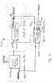
- FIG. 1 shows a block diagram of a memory system in accordance with the invention.
- FIG. 2 shows timing for the FIG. 1 system.
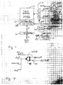
- FIG. 3 shows the refresh controller of the FIG. 1 system.
- FIG. 4 shows the arbiter of FIG. 1.
- a memory cell array contains 128K words of 32-bits.
- the array therefore has 32 data I/O lines.
- FIG. 1 shows an example of the present memory system with such an array. It includes the memory cell array 10, a memory array sequencer 14, a memory address multiplexer 16, a refresh controller 20, an external access controller 22 and an access arbiter 26.
- the memory array 10 is arranged into 2K rows and 2K columns. Associated with each column is a sense-amplifier in block 30 which performs the data sensing, restore and write operation. During each access, one cell array row is activated and the 2K memory cells of that row are connected to the sense-amplifiers 30 in each column.
- the sense-amplifiers 30 are conventionally connected to the I/O buffers 36 through a set of 2K-to-32 column multiplexers 38.
- the memory array sequencer 14 generates the conventional DRAM control signals RAS# and CAS# for controlling the operation of the array. Functions of the RAS# and CAS# signals are similar to those described in US Patent #5,615,169 to the same inventor, and incorporated by reference herein in its entirety.
- the external access controller 22 interprets external access commands and generates read/write requests. In one embodiment, two signals are used to determine an external access: Clock (CLK), and Address-Strobe (ADS#). The external access is detected at the rising clock edge on the activation of an Address-Strobe (ADS#) signal.
- FIG. 2 shows the timing relationship of these two signals.
- the ADS# and CLK signaling is similar to the industry standard for synchronous SRAM (See e.g. Pentium Processor 3.3v Pipelined BSRAM specification version 2.0 May 25, 1995, Intel).
- the external interface signal can be made similar to that of standard asynchronous SRAM (See Data sheet for M5M5178P, 64K SRAM, Mitsubishi Semiconductor Memory Data Book, 1990).
- the ADS# signal can be generated internally by an address transition detection circuit similar to the one described in "A 21-mW 4-Mb CMOS SRAM for Battery Operation” by Murakami et al., JSSC, Vol. 26, No, 11, pp. 1563-1567, November 1991.
- the ADS# signal thus generated can be used to synchronize the internal operation of the memory.
- the external-access controller 22 Upon the detection of an external access, the external-access controller 22 activates the request signal EREQ# to the access arbiter 26 which in turn drives the ASEL signal high to select an address on the External Access Address Bus ECAdd for the accessing address to the memory array 10.
- Arbiter 26 also activates the External Access EA# signal which is input to the memory array sequencer 14 for generating the RAS# and CAS# signals for controlling the array operations. The timing of these signals is also shown in FIG. 2.
- the access priority is always granted by arbiter 26 to the external access. By doing so, external accesses are not delayed by the refresh.
- This embodiment is configured to have the memory cycle time equal to a clock period, thus allowing a random access per clock cycle.
- the access is random, that is, it can be any address spanned by the device address space.
- the arbiter 26 evaluates the requests and drives the ASEL signal, input to the address multiplexer 16, to select one of the two addresses: refresh address RFAdd or external access address ECAdd to be used for the memory array 10 operation. Only in the absence of an external access does the arbiter 26 allow a refresh access to go through. In case of collisions, the refresh is delayed. The timing of this is also shown in FIG. 2.
- the refresh controller 20 generates refresh requests periodically so as to make sure that the memory array 10 is refreshed properly. Since the memory array 10 is refreshed one row of cells at a time, for a refresh time of 16ms, the refresh controller 20 generates one refresh request every 8 ⁇ s.
- the refresh request signal RREQ# is activated when there is a pending refresh. The activation of the RREQ# signal is detected by the arbiter 26 at the rising-edge of the MCLK signal. If no external access request is detected, the arbiter 26 drives both the Refresh Acknowledge RFACK# and ASEL signals low for one clock cycle. The former signals that the current memory cycle is used for refresh and the later selects the Refresh address from the refresh controller 20 as the address to the memory array 10.
- FIG. 3 shows a block diagram of the refresh controller 20, which includes a refresh address counter 40, a refresh timer 44 and a refresh accumulator 50.
- the refresh counter 40 provides the 11-bit row address to the memory array 10 during a refresh cycle.
- the refresh counter 40 is incremented at the end of the refresh cycle signaled by the deactivation of the refresh acknowledge RFACK#.
- the refresh timer 44 is reset (by the Reset signal) at power up.
- Timer 44 includes 12-bit counter 46 which provides a total count of 4095 cycles and a 12-input NAND gate 48. For a clock frequency of 100MHz, the timer 44 times up (signals QO-Q12 are high) approximately every 8 ⁇ s.
- the refresh up RFUP# signal is driven low by NAND gate 48 for one clock cycle.
- This signal is input to the refresh accumulator 50 for incrementing its 3-bit up/down counter 52.
- the up/down counter 52 increments by one when RFUP# is driven low and decrements by one when RFACK# is driven low for one clock cycle.
- the counter 52 stops incrementing when it reaches the full count, that is when AQ0-AQ2 are all high. If the accumulator 50 count is not empty, that is signals AQ0-AQ2 are not equal to 000, Refresh Request RRQg is asserted low by OR gate 54.
- the function of the accumulator 50 is illustrated as follows.
- the refresh requests are accumulated in the accumulator 50.
- the refresh request RREQ# signal to the arbiter 26 will continue to be asserted low until the accumulator 50 is empty.
- the accumulator 50 can accumulate up to 7 refreshes. This allows the system to continue external accesses for a period of up to 56 ⁇ s without losing refresh cycles.
- back-to-back external accesses longer than 56 ⁇ s in general do not occur.
- the counter 52 size can be increased or decreased to meet the application requirement.
- the signal MCLK which synchronizes the operations of the memory system is derived conventionally from the external clock signal CLK.
- MCLK can be generated by a conventional on-chip oscillator and PLL (phase locked loop). The PLL synchronizes the MCLK rising-edge to the output of the address transition detector which generates a pulse on the occurrence of a transition on the address bus.
- FIG. 4 shows an example of internal structure of arbiter 26 of FIG. 1, including in this embodiment a NAND gate 56 coupled as shown to inverter 58; thus refresh is prevented except in the absence of a pending memory array external access.
Landscapes
- Engineering & Computer Science (AREA)
- Microelectronics & Electronic Packaging (AREA)
- Computer Hardware Design (AREA)
- Dram (AREA)
- Semiconductor Memories (AREA)
Applications Claiming Priority (2)
| Application Number | Priority Date | Filing Date | Title |
|---|---|---|---|
| US37396 | 1998-03-09 | ||
| US09/037,396 US6028804A (en) | 1998-03-09 | 1998-03-09 | Method and apparatus for 1-T SRAM compatible memory |
Publications (2)
| Publication Number | Publication Date |
|---|---|
| EP0942430A1 true EP0942430A1 (fr) | 1999-09-15 |
| EP0942430B1 EP0942430B1 (fr) | 2006-08-23 |
Family
ID=21894121
Family Applications (1)
| Application Number | Title | Priority Date | Filing Date |
|---|---|---|---|
| EP99301728A Expired - Lifetime EP0942430B1 (fr) | 1998-03-09 | 1999-03-08 | Procédé et dispositif de mémoire compatible avec une 1-T SRAM |
Country Status (5)
| Country | Link |
|---|---|
| US (1) | US6028804A (fr) |
| EP (1) | EP0942430B1 (fr) |
| JP (1) | JPH11297067A (fr) |
| DE (1) | DE69932875T2 (fr) |
| TW (1) | TW434545B (fr) |
Cited By (7)
| Publication number | Priority date | Publication date | Assignee | Title |
|---|---|---|---|---|
| WO2002089140A3 (fr) * | 2001-05-01 | 2003-03-20 | Monolithic System Tech Inc | Procede et dispositif pour masquer completement des operations de rafraichissement dans une dram au moyen d'une division de signal d'horloge multiple |
| US6751157B2 (en) | 1998-10-01 | 2004-06-15 | Monolithic System Technology, Inc. | Method and apparatus for completely hiding refresh operations in a DRAM device using clock division |
| US6795364B1 (en) | 2003-02-28 | 2004-09-21 | Monolithic System Technology, Inc. | Method and apparatus for lengthening the data-retention time of a DRAM device in standby mode |
| US6898140B2 (en) | 1998-10-01 | 2005-05-24 | Monolithic System Technology, Inc. | Method and apparatus for temperature adaptive refresh in 1T-SRAM compatible memory using the subthreshold characteristics of MOSFET transistors |
| US7274618B2 (en) | 2005-06-24 | 2007-09-25 | Monolithic System Technology, Inc. | Word line driver for DRAM embedded in a logic process |
| US7535749B2 (en) | 1990-04-06 | 2009-05-19 | Mosaid Technologies, Inc. | Dynamic memory word line driver scheme |
| US7599246B2 (en) | 1994-10-06 | 2009-10-06 | Mosaid Technologies, Inc. | Delay locked loop implementation in a synchronous dynamic random access memory |
Families Citing this family (35)
| Publication number | Priority date | Publication date | Assignee | Title |
|---|---|---|---|---|
| US6496437B2 (en) | 1999-01-20 | 2002-12-17 | Monolithic Systems Technology, Inc. | Method and apparatus for forcing idle cycles to enable refresh operations in a semiconductor memory |
| JP4339995B2 (ja) | 1999-11-16 | 2009-10-07 | パナソニック株式会社 | 半導体記憶装置 |
| TW535161B (en) * | 1999-12-03 | 2003-06-01 | Nec Electronics Corp | Semiconductor memory device and its testing method |
| US6941415B1 (en) * | 2000-08-21 | 2005-09-06 | Micron Technology, Inc. | DRAM with hidden refresh |
| JP3726661B2 (ja) | 2000-09-01 | 2005-12-14 | セイコーエプソン株式会社 | 半導体メモリ装置のリフレッシュ制御 |
| JP3726660B2 (ja) | 2000-09-01 | 2005-12-14 | セイコーエプソン株式会社 | 半導体メモリ装置のリフレッシュ制御 |
| US6697909B1 (en) * | 2000-09-12 | 2004-02-24 | International Business Machines Corporation | Method and apparatus for performing data access and refresh operations in different sub-arrays of a DRAM cache memory |
| JP3627647B2 (ja) | 2000-10-27 | 2005-03-09 | セイコーエプソン株式会社 | 半導体メモリ装置内のワード線の活性化 |
| JP3705113B2 (ja) | 2000-10-27 | 2005-10-12 | セイコーエプソン株式会社 | 半導体メモリ装置内のワード線の活性化 |
| JP3531602B2 (ja) | 2000-11-08 | 2004-05-31 | セイコーエプソン株式会社 | 半導体メモリ装置内のワード線の活性化 |
| JP3967559B2 (ja) * | 2001-04-06 | 2007-08-29 | 富士通株式会社 | 制御回路及び半導体記憶装置 |
| JP2002313079A (ja) | 2001-04-18 | 2002-10-25 | Seiko Epson Corp | 半導体メモリ装置の電源ノイズの抑制化 |
| KR100394322B1 (ko) * | 2001-05-19 | 2003-08-09 | (주)이엠엘에스아이 | 리프레쉬 동작을 제어할 수 있는 디램 셀을 이용한 에스램호환 메모리 장치 |
| KR100394587B1 (ko) * | 2001-05-19 | 2003-08-14 | (주)실리콘세븐 | 디램 셀을 이용한 에스램 호환 메모리 장치의 리프레쉬 회로 |
| KR100401235B1 (ko) * | 2001-05-22 | 2003-10-17 | (주)실리콘세븐 | 디램 셀을 이용한 에스램 호환 메모리 장치의 로우 제어회로 |
| JP4743999B2 (ja) * | 2001-05-28 | 2011-08-10 | ルネサスエレクトロニクス株式会社 | 半導体記憶装置 |
| JP3985889B2 (ja) | 2001-08-08 | 2007-10-03 | 株式会社ルネサステクノロジ | 半導体装置 |
| TW533413B (en) * | 2001-10-11 | 2003-05-21 | Cascade Semiconductor Corp | Asynchronous hidden refresh of semiconductor memory |
| US6625077B2 (en) * | 2001-10-11 | 2003-09-23 | Cascade Semiconductor Corporation | Asynchronous hidden refresh of semiconductor memory |
| US6643732B1 (en) | 2001-11-14 | 2003-11-04 | Etron Technology, Inc. | Delayed read/write scheme for SRAM interface compatible DRAM |
| US6735139B2 (en) * | 2001-12-14 | 2004-05-11 | Silicon Storage Technology, Inc. | System and method for providing asynchronous SRAM functionality with a DRAM array |
| JP2003196977A (ja) * | 2001-12-27 | 2003-07-11 | Fujitsu Ltd | 半導体記憶装置のデータアクセス方法、及び半導体記憶装置 |
| US6638813B1 (en) | 2002-01-29 | 2003-10-28 | Taiwan Semiconductor Manufacturing Company | Method of forming a composite spacer to eliminate polysilicon stringers between elements in a pseudo SRAM cell |
| JP4078119B2 (ja) * | 2002-04-15 | 2008-04-23 | 富士通株式会社 | 半導体メモリ |
| KR100481819B1 (ko) * | 2002-08-27 | 2005-04-11 | (주)실리콘세븐 | 디램 셀을 사용하며, 칩 디스에이블 구간 중에 발생하는신호에 의하여 리프레쉬가 수행되도록 제어되는 동기식에스램 호한 메모리 |
| JP3705276B2 (ja) | 2003-04-21 | 2005-10-12 | セイコーエプソン株式会社 | 半導体メモリ装置におけるリフレッシュ制御および内部電圧の生成 |
| KR100525459B1 (ko) * | 2003-05-16 | 2005-10-31 | (주)실리콘세븐 | 인출과 기입 동작 구간이 분리되는 리프레쉬 동작을수행하는 에스램 호환 메모리 및 그 구동방법 |
| US20050229959A1 (en) * | 2004-04-16 | 2005-10-20 | Chen-Hsiung Lin | Sunshade structure |
| US7113439B2 (en) * | 2004-04-22 | 2006-09-26 | Memocom Corp. | Refresh methods for RAM cells featuring high speed access |
| US7433996B2 (en) * | 2004-07-01 | 2008-10-07 | Memocom Corp. | System and method for refreshing random access memory cells |
| US7532532B2 (en) * | 2005-05-31 | 2009-05-12 | Micron Technology, Inc. | System and method for hidden-refresh rate modification |
| US7499307B2 (en) * | 2005-06-24 | 2009-03-03 | Mosys, Inc. | Scalable embedded DRAM array |
| US7533222B2 (en) * | 2006-06-29 | 2009-05-12 | Mosys, Inc. | Dual-port SRAM memory using single-port memory cell |
| KR20170025896A (ko) * | 2015-08-31 | 2017-03-08 | 에스케이하이닉스 주식회사 | 반도체 장치 및 이를 포함하는 반도체 시스템 |
| US10394719B2 (en) | 2017-01-25 | 2019-08-27 | Samsung Electronics Co., Ltd. | Refresh aware replacement policy for volatile memory cache |
Citations (4)
| Publication number | Priority date | Publication date | Assignee | Title |
|---|---|---|---|---|
| US4549284A (en) * | 1982-03-10 | 1985-10-22 | Hitachi, Ltd. | Dynamic MOS random access memory |
| EP0588250A2 (fr) * | 1992-09-18 | 1994-03-23 | New Media Corporation | Circuit de commande de rafraîchissement pour PSRAM |
| US5544120A (en) * | 1993-04-07 | 1996-08-06 | Kabushiki Kaisha Toshiba | Semiconductor integrated circuit including ring oscillator of low current consumption |
| US5586287A (en) * | 1994-05-13 | 1996-12-17 | Sharp Kabushiki Kaisha | Information processing apparatus capable of holding storage contents of PSRAM even when system clock comes to abnormal halt |
Family Cites Families (2)
| Publication number | Priority date | Publication date | Assignee | Title |
|---|---|---|---|---|
| US4625301A (en) * | 1983-11-30 | 1986-11-25 | Tandy Corporation | Dynamic memory refresh circuit |
| KR950014089B1 (ko) * | 1993-11-08 | 1995-11-21 | 현대전자산업주식회사 | 동기식 디램의 히든 셀프 리프레쉬 방법 및 장치 |
-
1998
- 1998-03-09 US US09/037,396 patent/US6028804A/en not_active Expired - Lifetime
-
1999
- 1999-02-23 TW TW088102687A patent/TW434545B/zh not_active IP Right Cessation
- 1999-03-08 DE DE69932875T patent/DE69932875T2/de not_active Expired - Lifetime
- 1999-03-08 EP EP99301728A patent/EP0942430B1/fr not_active Expired - Lifetime
- 1999-03-09 JP JP11061012A patent/JPH11297067A/ja active Pending
Patent Citations (4)
| Publication number | Priority date | Publication date | Assignee | Title |
|---|---|---|---|---|
| US4549284A (en) * | 1982-03-10 | 1985-10-22 | Hitachi, Ltd. | Dynamic MOS random access memory |
| EP0588250A2 (fr) * | 1992-09-18 | 1994-03-23 | New Media Corporation | Circuit de commande de rafraîchissement pour PSRAM |
| US5544120A (en) * | 1993-04-07 | 1996-08-06 | Kabushiki Kaisha Toshiba | Semiconductor integrated circuit including ring oscillator of low current consumption |
| US5586287A (en) * | 1994-05-13 | 1996-12-17 | Sharp Kabushiki Kaisha | Information processing apparatus capable of holding storage contents of PSRAM even when system clock comes to abnormal halt |
Cited By (12)
| Publication number | Priority date | Publication date | Assignee | Title |
|---|---|---|---|---|
| US7535749B2 (en) | 1990-04-06 | 2009-05-19 | Mosaid Technologies, Inc. | Dynamic memory word line driver scheme |
| US8023314B2 (en) | 1990-04-06 | 2011-09-20 | Mosaid Technologies Incorporated | Dynamic memory word line driver scheme |
| US7599246B2 (en) | 1994-10-06 | 2009-10-06 | Mosaid Technologies, Inc. | Delay locked loop implementation in a synchronous dynamic random access memory |
| US8369182B2 (en) | 1994-10-06 | 2013-02-05 | Mosaid Technologies Incorporated | Delay locked loop implementation in a synchronous dynamic random access memory |
| US8638638B2 (en) | 1994-10-06 | 2014-01-28 | Mosaid Technologies Incorporated | Delay locked loop implementation in a synchronous dynamic random access memory |
| US6707743B2 (en) | 1998-10-01 | 2004-03-16 | Monolithic System Technology, Inc. | Method and apparatus for completely hiding refresh operations in a DRAM device using multiple clock division |
| US6751157B2 (en) | 1998-10-01 | 2004-06-15 | Monolithic System Technology, Inc. | Method and apparatus for completely hiding refresh operations in a DRAM device using clock division |
| US6898140B2 (en) | 1998-10-01 | 2005-05-24 | Monolithic System Technology, Inc. | Method and apparatus for temperature adaptive refresh in 1T-SRAM compatible memory using the subthreshold characteristics of MOSFET transistors |
| WO2002089140A3 (fr) * | 2001-05-01 | 2003-03-20 | Monolithic System Tech Inc | Procede et dispositif pour masquer completement des operations de rafraichissement dans une dram au moyen d'une division de signal d'horloge multiple |
| US6795364B1 (en) | 2003-02-28 | 2004-09-21 | Monolithic System Technology, Inc. | Method and apparatus for lengthening the data-retention time of a DRAM device in standby mode |
| US7274618B2 (en) | 2005-06-24 | 2007-09-25 | Monolithic System Technology, Inc. | Word line driver for DRAM embedded in a logic process |
| US7447104B2 (en) | 2005-06-24 | 2008-11-04 | Mosys, Inc. | Word line driver for DRAM embedded in a logic process |
Also Published As
| Publication number | Publication date |
|---|---|
| DE69932875T2 (de) | 2006-12-21 |
| JPH11297067A (ja) | 1999-10-29 |
| TW434545B (en) | 2001-05-16 |
| DE69932875D1 (de) | 2006-10-05 |
| EP0942430B1 (fr) | 2006-08-23 |
| US6028804A (en) | 2000-02-22 |
Similar Documents
| Publication | Publication Date | Title |
|---|---|---|
| EP0942430B1 (fr) | Procédé et dispositif de mémoire compatible avec une 1-T SRAM | |
| US6496437B2 (en) | Method and apparatus for forcing idle cycles to enable refresh operations in a semiconductor memory | |
| US6222785B1 (en) | Method and apparatus for refreshing a semiconductor memory using idle memory cycles | |
| US7640391B2 (en) | Integrated circuit random access memory capable of automatic internal refresh of memory array | |
| KR100987997B1 (ko) | 반도체 메모리 및 시스템 | |
| US9570144B2 (en) | Memory refresh method and devices | |
| US6463001B1 (en) | Circuit and method for merging refresh and access operations for a memory device | |
| US20050108460A1 (en) | Partial bank DRAM refresh | |
| US20030231540A1 (en) | DRAM with total self refresh and control circuit | |
| US20060143372A1 (en) | Directed auto-refresh synchronization | |
| US5583823A (en) | Dram refresh circuit | |
| US6859407B1 (en) | Memory with auto refresh to designated banks | |
| US5943681A (en) | Semiconductor memory device having cache function | |
| US20050105357A1 (en) | Method and circuit configuration for refreshing data in a semiconductor memory | |
| US6941415B1 (en) | DRAM with hidden refresh | |
| EP1384231B1 (fr) | Procédé et dispositif pour masquer complétement des opérations de rafraîchissement dans une dram au moyen d'une division de signal d'horloge multiple | |
| US20060190678A1 (en) | Static random access memory (SRAM) compatible, high availability memory array and method employing synchronous dynamic random access memory (DRAM) in conjunction with a single DRAM cache and tag | |
| KR20250135677A (ko) | 반도체 기억장치 및 이의 제어 방법 | |
| JPH04132078A (ja) | メモリリフレッシュ方式 | |
| Zhang | A study of DRAM optimization to break the Memory Wall | |
| KR20030091431A (ko) | 감소된 랜덤 억세스 타임을 갖는 비동기 반도체 메모리장치 및 그에 따른 랜덤 억세스 타임 감소방법 |
Legal Events
| Date | Code | Title | Description |
|---|---|---|---|
| PUAI | Public reference made under article 153(3) epc to a published international application that has entered the european phase |
Free format text: ORIGINAL CODE: 0009012 |
|
| AK | Designated contracting states |
Kind code of ref document: A1 Designated state(s): DE FR GB |
|
| AX | Request for extension of the european patent |
Free format text: AL;LT;LV;MK;RO;SI |
|
| RAP1 | Party data changed (applicant data changed or rights of an application transferred) |
Owner name: MONOLITHIC SYSTEM TECHNOLOGY, INC. |
|
| 17P | Request for examination filed |
Effective date: 19991208 |
|
| AKX | Designation fees paid |
Free format text: DE FR GB |
|
| 17Q | First examination report despatched |
Effective date: 20040330 |
|
| GRAP | Despatch of communication of intention to grant a patent |
Free format text: ORIGINAL CODE: EPIDOSNIGR1 |
|
| GRAS | Grant fee paid |
Free format text: ORIGINAL CODE: EPIDOSNIGR3 |
|
| GRAA | (expected) grant |
Free format text: ORIGINAL CODE: 0009210 |
|
| AK | Designated contracting states |
Kind code of ref document: B1 Designated state(s): DE FR GB |
|
| REG | Reference to a national code |
Ref country code: GB Ref legal event code: FG4D |
|
| REF | Corresponds to: |
Ref document number: 69932875 Country of ref document: DE Date of ref document: 20061005 Kind code of ref document: P |
|
| ET | Fr: translation filed | ||
| PLBE | No opposition filed within time limit |
Free format text: ORIGINAL CODE: 0009261 |
|
| STAA | Information on the status of an ep patent application or granted ep patent |
Free format text: STATUS: NO OPPOSITION FILED WITHIN TIME LIMIT |
|
| 26N | No opposition filed |
Effective date: 20070524 |
|
| REG | Reference to a national code |
Ref country code: DE Ref legal event code: R082 Ref document number: 69932875 Country of ref document: DE Representative=s name: WILHELMS, KILIAN & PARTNER, DE Ref country code: DE Ref legal event code: R082 Ref document number: 69932875 Country of ref document: DE Representative=s name: BOSCH JEHLE PATENTANWALTSGESELLSCHAFT MBH, DE |
|
| REG | Reference to a national code |
Ref country code: DE Ref legal event code: R082 Ref document number: 69932875 Country of ref document: DE Representative=s name: BOSCH JEHLE PATENTANWALTSGESELLSCHAFT MBH, DE |
|
| REG | Reference to a national code |
Ref country code: GB Ref legal event code: 732E Free format text: REGISTERED BETWEEN 20120705 AND 20120711 |
|
| REG | Reference to a national code |
Ref country code: DE Ref legal event code: R082 Ref document number: 69932875 Country of ref document: DE Representative=s name: BOSCH JEHLE PATENTANWALTSGESELLSCHAFT MBH, DE Effective date: 20120611 Ref country code: DE Ref legal event code: R082 Ref document number: 69932875 Country of ref document: DE Representative=s name: BOSCH JEHLE PATENTANWALTSGESELLSCHAFT MBH, DE Effective date: 20120302 Ref country code: DE Ref legal event code: R081 Ref document number: 69932875 Country of ref document: DE Owner name: INVENSAS CORP., SAN JOSE, US Free format text: FORMER OWNER: MONOLITHIC SYSTEM TECHNOLOGY, INC., SUNNYVALE, CALIF., US Effective date: 20120611 Ref country code: DE Ref legal event code: R081 Ref document number: 69932875 Country of ref document: DE Owner name: INVENSAS CORP., US Free format text: FORMER OWNER: MONOLITHIC SYSTEM TECHNOLOGY, INC., SUNNYVALE, US Effective date: 20120611 |
|
| REG | Reference to a national code |
Ref country code: FR Ref legal event code: TP Owner name: INVENSAS CORPORATION, US Effective date: 20120720 Ref country code: FR Ref legal event code: CD Owner name: INVENSAS CORPORATION, US Effective date: 20120720 |
|
| REG | Reference to a national code |
Ref country code: FR Ref legal event code: PLFP Year of fee payment: 17 |
|
| REG | Reference to a national code |
Ref country code: FR Ref legal event code: PLFP Year of fee payment: 18 |
|
| REG | Reference to a national code |
Ref country code: FR Ref legal event code: PLFP Year of fee payment: 19 |
|
| REG | Reference to a national code |
Ref country code: FR Ref legal event code: PLFP Year of fee payment: 20 |
|
| PGFP | Annual fee paid to national office [announced via postgrant information from national office to epo] |
Ref country code: GB Payment date: 20180327 Year of fee payment: 20 |
|
| PGFP | Annual fee paid to national office [announced via postgrant information from national office to epo] |
Ref country code: FR Payment date: 20180326 Year of fee payment: 20 |
|
| PGFP | Annual fee paid to national office [announced via postgrant information from national office to epo] |
Ref country code: DE Payment date: 20180328 Year of fee payment: 20 |
|
| REG | Reference to a national code |
Ref country code: DE Ref legal event code: R071 Ref document number: 69932875 Country of ref document: DE |
|
| REG | Reference to a national code |
Ref country code: GB Ref legal event code: PE20 Expiry date: 20190307 |
|
| PG25 | Lapsed in a contracting state [announced via postgrant information from national office to epo] |
Ref country code: GB Free format text: LAPSE BECAUSE OF EXPIRATION OF PROTECTION Effective date: 20190307 |