EP0588250A2 - Circuit de commande de rafraîchissement pour PSRAM - Google Patents
Circuit de commande de rafraîchissement pour PSRAM Download PDFInfo
- Publication number
- EP0588250A2 EP0588250A2 EP93114547A EP93114547A EP0588250A2 EP 0588250 A2 EP0588250 A2 EP 0588250A2 EP 93114547 A EP93114547 A EP 93114547A EP 93114547 A EP93114547 A EP 93114547A EP 0588250 A2 EP0588250 A2 EP 0588250A2
- Authority
- EP
- European Patent Office
- Prior art keywords
- memory
- refresh
- controller
- delay line
- pseudo
- Prior art date
- Legal status (The legal status is an assumption and is not a legal conclusion. Google has not performed a legal analysis and makes no representation as to the accuracy of the status listed.)
- Withdrawn
Links
Images

Classifications
-
- G—PHYSICS
- G11—INFORMATION STORAGE
- G11C—STATIC STORES
- G11C11/00—Digital stores characterised by the use of particular electric or magnetic storage elements; Storage elements therefor
- G11C11/21—Digital stores characterised by the use of particular electric or magnetic storage elements; Storage elements therefor using electric elements
- G11C11/34—Digital stores characterised by the use of particular electric or magnetic storage elements; Storage elements therefor using electric elements using semiconductor devices
- G11C11/40—Digital stores characterised by the use of particular electric or magnetic storage elements; Storage elements therefor using electric elements using semiconductor devices using transistors
- G11C11/401—Digital stores characterised by the use of particular electric or magnetic storage elements; Storage elements therefor using electric elements using semiconductor devices using transistors forming cells needing refreshing or charge regeneration, i.e. dynamic cells
- G11C11/406—Management or control of the refreshing or charge-regeneration cycles
- G11C11/40615—Internal triggering or timing of refresh, e.g. hidden refresh, self refresh, pseudo-SRAMs
-
- G—PHYSICS
- G11—INFORMATION STORAGE
- G11C—STATIC STORES
- G11C11/00—Digital stores characterised by the use of particular electric or magnetic storage elements; Storage elements therefor
- G11C11/21—Digital stores characterised by the use of particular electric or magnetic storage elements; Storage elements therefor using electric elements
- G11C11/34—Digital stores characterised by the use of particular electric or magnetic storage elements; Storage elements therefor using electric elements using semiconductor devices
- G11C11/40—Digital stores characterised by the use of particular electric or magnetic storage elements; Storage elements therefor using electric elements using semiconductor devices using transistors
- G11C11/401—Digital stores characterised by the use of particular electric or magnetic storage elements; Storage elements therefor using electric elements using semiconductor devices using transistors forming cells needing refreshing or charge regeneration, i.e. dynamic cells
- G11C11/406—Management or control of the refreshing or charge-regeneration cycles
Definitions
- This invention relates to random access memories, and, more particularly, to the efficient utilization of a pseudo-static random access memory that must be periodically refreshed to avoid the loss of information stored in the memory.
- RAM Random Access Memory
- Static Random Access Memory retains information in memory for an indefinite period of time without refreshing (recharging) of the state of the individual memory cells.
- Dynamic Random Access Memory retains information in memory only as long as the memory cells are continually refreshed.
- SRAM requires relatively complex individual memory cells, which are expensive and occupy large areas on chips or cards. DRAM is less expensive and space consuming, but requires potentially complex refresh circuitry that may be expensive and may slow the access of the host processor to the memory cell.
- SRAM has a low current consumption because it need not be refreshed, while DRAM has a relatively high current consumption because of the need for continual refreshing.
- PSRAM Pseudo-Static Random Access Memory
- the PSRAM has a simpler memory cell than the SRAM, and is therefore less-expensive and smaller than the SRAM.
- the PSRAM requires periodic rather than continual refreshing, as is the case for DRAM.
- PSRAM is provided with internal refresh circuitry, and therefore requires less complex external refresh circuitry and permits better memory access for the host processor than DRAM.
- PSRAM provides the cost effectiveness of DRAM with the implementation ease of SRAM.
- PSRAM has a current consumption intermediate that of SRAM and DRAM, and is acceptable for use in both desk top and portable devices requiring memory.
- PSRAM memory is available in standard memory sizes from a number of manufacturers, including, for example, Hitachi, Toshiba, Samsung, and NEC.
- the PSRAM may perform far too many refresh cycles with some of the refresh cycles being performed when the processor seeks access to the memory. In each case the processor eventually gains access to the memory through an interruption of the refresh cycles. However, the processor is denied access to memory when the refresh cycles are being performed, slowing down the overall performance of the system.
- the delays in access to memory occasioned by the need to refresh the PSRAM, though individually small, can accumulate to have a significant effect on the speed of the processor system. Excessive numbers of refresh cycles also can consume excessive power, an important consideration if the PSRAM is used in a portable, battery-powered device.
- the present invention fulfills this need, and further provides related advantages.
- the present invention provides a controller for PSRAM refresh.
- the controller is utilized in a system having a remote processor wherein timing signals are not available to the controller. Instead, the controller optimizes system performance utilizing only memory control information available on the memory bus.
- the controller minimizes the waiting time for the host processor to perform memory access cycles, while achieving the required refresh cycles of the PSRAM by applying required refresh cycles during the time the host is known not to access the memory and at other times as required by the PSRAM devices.
- the present approach is particularly useful where the PSRAM is located on a removable card that can be plugged into the unit containing the host. Only signals generally available on the host processor bus are required to accomplish PSRAM refresh control.
- a controller controls the refreshing of a pseudo-static random access memory accessible from a remote host processor.
- the controller comprises means for asynchronously detecting a memory enabling/disabling signal of a host processor, and means for initiating a synchronous automatic refresh of a pseudo-static random access memory upon receipt from the means for asynchronously detecting of an indication of detection of a memory enabling/disabling signal.
- the memory enabling/disabling signal is a change-of-state signal transmitted across the bus from the host processor to the memory, and can be detected by elements physically associated with the memory.
- the memory enabling/disabling signal may be associated with the beginning or the end of a memory access cycle. When it is associated with the beginning of the memory access cycle, with some processors there may be a delay of up to several hundred nanoseconds after the transmission of the memory enabling/disabling signal and the beginning of the memory access. In such processors, an automatic refresh can be accomplished during that period, which otherwise is an idle period. (In other processors, the time between the transmission of the memory enabling/disabling signal and the start of the memory access is too short to reasonably accomplish a refresh cycle, and this aspect of the present invention would not be used.)
- a controller refreshes a pseudo-static random access memory (PSRAM) accessible from a remote host processor.
- the controller comprises means for asynchronously detecting the end of a memory access cycle by a host processor and means for generating output signals at preselected times after activation by the means for asynchronously detecting the end of a memory access cycle.
- the output signals include a first output signal and a second output signal a sufficient time after the first timed output signal to permit performance of an automatic refresh of the PSRAM.
- the controller further includes means for initiating an automatic refresh of the PSRAM upon receipt of the first timed output signal and means for discontinuing the automatic refresh of the PSRAM upon receipt of the second timed output signal.
- the controller utilizes a tapped delay line to generate the output signals.
- the controller includes means for asynchronously detecting the end of a memory access cycle by a host processor and a tapped delay line activated by the means for asynchronously detecting upon detection of the end of a memory access cycle of the PSRAM by the host processor.
- the tapped delay line produces a series of delay line output signals at a series of preselected times after activation.
- the controller further includes means for initiating an automatic refresh of the PSRAM upon receipt of a first tapped delay line output signal and means for discontinuing the automatic refresh of the PSRAM upon receipt of a second tapped delay line output signal that follows the first tapped delay line output signal by a sufficient time to permit performance of an automatic refresh.
- a tapped delay line has the important advantage that it is not necessary to wait to begin the refresh cycle until clock pulsing can be synchronized with the refresh cycle, which may require up to a full clock cycle with each refresh cycle performed. Instead, the refresh cycle begins immediately and, in a statistical sense, can be completed most rapidly from the time that PSRAM becomes available for refresh (after completion of a memory access cycle by the host processor).
- the controller permits memory access by the host processor. If the host processor seeks access, further refresh cycles are not performed and the host is allowed access to the memory. If the host processor does not seek access during that time period, a further refresh cycle may be performed immediately after the completion of the prior refresh cycle. This strategy may, however, lead to overly many refresh cycles, which consume an unnecessarily large amount of power in PSRAM refresh. A mandatory delay between refresh cycles may therefore be implemented, even when the host processor does not demand access to the memory.
- a major benefit of inserting a refresh cycle immediately after a memory access cycle begins or ends is that in nearly all systems, the host processor is known not to require memory access for some period of time immediately thereafter. If this time is the same as or greater than the time required for an automatic refresh cycle, there is no impact on the performance of the system of insertion of an automatic refresh cycle at this point. For specific processor systems, there are additional times that the host processor is known not to require memory access. These times can be determined by the memory bus control signals. In these cases, the refresh cycles may be inserted at these times instead of necessarily at the end of the memory access cycle for transparent refresh cycles.
- the present invention provides an important advance in the art of PSRAM utilization in host processor/PSRAM, systems. Memory access time for the processor is optimized, consistent with the requirement for PSRAM refresh. The result is that inexpensive, small-size PSRAM may be used with improved net system performance as compared with conventional PSRAM application.
- FIG. 1 shows the circuit arrangement for a preferred host-processor/PSRAM system 20 in which the controller of the invention is used.
- a central processing unit (CPU) 22 is connected to a memory card 24 by a bus 26.
- the memory card 24 has available only the signals on the bus 26, not the internal timing and state signals of the CPU 22. This is termed a “remote” or "host” processor system.
- the memory card 24 has a number of PSRAM chips 28, here illustrated as eight 512K PSRAM chips 28. These chips are available commercially from a number of manufacturers, such as Hitachi, Toshiba, Samsung, and NEC. A working embodiment of the present invention has been implemented using a Model HM658512 PSRAM chip available from Hitachi. A conventional address decoder 30 permits access to the PSRAM chips 28 by the CPU 22. The address decoder 30 is commercially available from a number of manufacturers, and for the working embodiment a Model SN74HC139 address decoder made by Texas Instruments has been used.
- the controller 32 also controls access of the CPU 22 to the PSRAM chips 28 in conjunction with the accomplishment of the refresh cycles.
- the controller 32 has been implemented as a programmable array logic (PAL) device Model AMPAlCE16V8 made by Advance Micro Devices as a standard programmable component.
- the controller 32 utilizes a tapped delay line 34 in the manner to be discussed.
- the tapped delay line 34 is available as a commercial component.
- a Model DS1000-200 tapped delay line made by Dallas Semiconductor was used.
- the PSRAM chips 28 must be refreshed with 2048 refresh cycles every 32 milliseconds. These particular values may vary for other designs, but may be taken as illustrative. Many strategies for refresh may be implemented. For example, the refresh cycles could be evenly distributed during the 32 millisecond period. In another approach, the refresh cycles could occur continuously, except for a period of a memory access interrupt by the CPU 22. In each case, such a strategy could lead to a reduced operating speed of the system 20 because the CPU 22 may have to consistently wait for overly long periods to gain memory access.
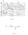
- FIG. 2 A single optimized refresh cycle for the 512K x 8 PSRAM memory of Figure 1 is illustrated in Figure 2.
- Each refresh cycle requires 160 nanoseconds.
- the refresh cycle begins when both the chip enable (CE) signal and the output enable (OE) states become inactive, indicating that the CPU 22 is not seeking to access the memory 28.
- CE chip enable
- OE output enable
- the refresh cycle is completed in another 80 nanoseconds, and both CE and OE must go inactive for an additional 40 nanoseconds to allow the device to recover from refresh.
- the memory 28 is unavailable to the CPU 22 during this 160 nanosecond period.
- the chip enable CE signal is a memory enabling/disabling signal. It is active when the host CPU 22 seeks access to the memory, and inactive when the host CPU 22 does not seek access to the memory. The transitions between inactive and active, and between active and inactive, are associated with the start and end of a memory access cycle, respectively.
- the card enable (CE1 and CE2), the output enable (OE), and the write enable (WE) signals are all generated by the host CPU 22 to request read and write cycles of the memory system. These signals are available on the bus 26, and are the only signals that the controller 32 receives from the CPU 22. Specifically, the controller 32 does not receive synchronous (clock) timing signals or other processor state information from the CPU 22 that could otherwise be used as an aid in controlling the refresh cycle.
- the internal chip enables (ICEU and ICEL), the internal output enable (IOE), and the internal write enable (IWE) signals are all generated by the controller 32 for memory control.
- ICEU is the chip enable for the upper 8 bits of the 16-bit word
- ICEL is the chip enable for the lower 8 bits of the 16-bit word.
- the primary timing control signal T0 is generated by the controller 32 and sent to the tapped delay line 34. Responsive to this signal T0, the delay line 34 generates a series of five delay line output signals T1, T2, T3, T4, and T5, at 40, 80, 120, 160, and 200 nanoseconds, respectively, after receipt of signal T0 by the delay line 34.
- timing devices could be used to provide timed output signals.
- the memory card 24 could be provided with an onboard general purpose clock instead of the delay line 34.
- the use of a clock is not preferred, however, because it would be necessary to synchronize the phase relationship of the clock with the CPU 22 and wait until the clock is in the proper state before commencing the refresh cycle.
- the timing is generated asynchronously, and it is therefore possible to begin the refresh cycle of the PSRAM immediately after a memory access cycle has been completed.
- the CPU 22 indicates the end of a memory access cycle by sending CE1 and CE2 inactive, numeral 40.
- the leading edge of the state transition is detected, sending T0 high, numeral 42, ICEU and ICEL high, numeral 44, and IOE high, numeral 46, to begin a refresh cycle.
- T0 is high
- a refresh cycle is underway, and the CPU 22 is denied access to the memory 28.
- the refresh cycle begins immediately after completion of the memory access cycle, due to the use of the delay line. There is no need to wait up to one clock cycle, as would be the case if a general purpose clock were used to generate timed output signals.
- the T0 rising edge produced by the controller 32 is introduced into the delay line 34, which produces delay line output signals at T1 (40 nanoseconds after T0), T2 (80 nanoseconds), T3 (120 nanoseconds), T4 (160 nanoseconds), and T5 (200 nanoseconds).
- T1 40 nanoseconds after T0
- T2 80 nanoseconds
- T3 120 nanoseconds
- T4 160 nanoseconds
- T5 200 nanoseconds
- the CPU 22 is permitted to request access to the memory 28 when T4 is high. If the card enables CE1 and CE2 have not gone low to indicate a requested access by the CPU 22 before T4 goes low, numeral 52, another refresh cycle is initiated when T5 goes low, numeral 54. Thus, in this case T5 becomes a refresh initiation signal for a further automatic refresh cycle, following immediately after the preceding automatic refresh cycle.
- the succession of automatic refresh cycles continues according to this strategy until the CPU 22 has requested access while T4 is high.
- the maximum time that the CPU 22 must wait for access to memory is therefore 160 nanoseconds, like other refresh schemes, but for consecutive memory access cycles the overhead is nearly zero nanoseconds.
- CE1 and CE2 go low while T1 is high (a refresh cycle is occurring), indicating a request for access by the CPU 22 to the memory 28, WAIT goes active, numeral 56, and stays active until the refresh cycle then being executed has been completed. After that particular refresh cycle has been completed, the CPU 22 is allowed access to the memory 28. If either the WE or OE signals goes active during a refresh cycle, they are not permitted to go to the memory chips 28 via either IEW or IOE until after the refresh cycle then being performed has ended, numeral 58. After any memory access cycle by the CPU 22 has ended and the card enables CE1 and CE2 go high, another refresh cycle may commence according to the steps discussed earlier.
- This preferred timing diagram was designed for a desk top computer where the principal concern is performance and access, not power consumption. Under this strategy, many more refreshes of the PSRAM 28 may be performed than is required to prevent loss of information. As a result, more power may be consumed in performing refresh cycles than is absolutely required.
- a mandatory delay between refresh cycles may be introduced.
- a preferred approach is to use the delay generator, of Figure 4 (again avoiding the need for an onboard clock).
- the self refresh mode available in commercial PSRAM chips can also be utilized wherever possible, depending upon the access demands of the host CPU 22. That is, the controller 32 is of most value when refresh is required interspersed with significant memory access requirements of the host processor. Where, for example, the CPU is inactive and waiting for instructions, conventional self refresh mode may employed. Timing and access requirements are not a concern in this mode. After a period of self refreshment operation using the timer previously described, the card can be placed into an extended self refresh mode. After the CPU again demands access, requiring the system to "wake up”, WAIT is asserted for a sufficient period, typically 600 nanoseconds, to permit the PSRAM chip 28 to recover from self refresh mode.
- the fast refresh mode of Figure 3 would be required for the next several milliseconds to ensure no loss of information in memory. Thereafter the card 24 returns to the slowed refresh mode using the timer of Figure 4 and then, if further access by the CPU is not demanded, back to the internal self refreshment mode.
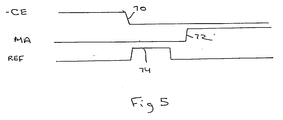
- a memory access cycle begins with the chip enable CE signal becoming active, numeral 70.
- a PSRAM automatic refresh cycle REF numeral 74
- the details of the automatic refresh cycle are as discussed in relation to Figure 2.
- the present invention therefore provides a highly versatile controller for optimizing the operation and access of the CPU to the information stored in PSRAM, while ensuring refreshment of the PSRAM and minimizing power consumption if necessary.
- the invention has been implemented in the fully hardware configuration depicted herein through the use of the described logic, and has been found fully operable.
- the controller 32, the PSRAM 28, the decoder 30, and the tapped delay line 34 are all mounted on the card 24 that can be plugged into a processor system.
- a connector 36 is placed between the card 24 and the bus 26/CPU 22. The card is simply plugged into the system to provide additional PSRAM with the automatic refreshing features discussed herein.
Landscapes
- Engineering & Computer Science (AREA)
- Microelectronics & Electronic Packaging (AREA)
- Computer Hardware Design (AREA)
- Dram (AREA)
Applications Claiming Priority (2)
| Application Number | Priority Date | Filing Date | Title |
|---|---|---|---|
| US947182 | 1992-09-18 | ||
| US07/947,182 US5617551A (en) | 1992-09-18 | 1992-09-18 | Controller for refreshing a PSRAM using individual automatic refresh cycles |
Publications (2)
| Publication Number | Publication Date |
|---|---|
| EP0588250A2 true EP0588250A2 (fr) | 1994-03-23 |
| EP0588250A3 EP0588250A3 (fr) | 1994-11-30 |
Family
ID=25485679
Family Applications (1)
| Application Number | Title | Priority Date | Filing Date |
|---|---|---|---|
| EP19930114547 Withdrawn EP0588250A3 (fr) | 1992-09-18 | 1993-09-10 | Circuit de commande de rafraîchissement pour PSRAM. |
Country Status (2)
| Country | Link |
|---|---|
| US (1) | US5617551A (fr) |
| EP (1) | EP0588250A3 (fr) |
Cited By (9)
| Publication number | Priority date | Publication date | Assignee | Title |
|---|---|---|---|---|
| EP0942430A1 (fr) * | 1998-03-09 | 1999-09-15 | MoSys, Inc. | Procédé et dispositif de mémoire compatible avec une 1-T SRAM |
| EP0851428A3 (fr) * | 1996-12-23 | 1999-10-27 | International Business Machines Corporation | Restauration conditionnelle pour unité d'exécution |
| US6415353B1 (en) | 1998-10-01 | 2002-07-02 | Monolithic System Technology, Inc. | Read/write buffers for complete hiding of the refresh of a semiconductor memory and method of operating same |
| US6449685B1 (en) | 1998-10-01 | 2002-09-10 | Monolithic System Technology, Inc. | Read/write buffers for complete hiding of the refresh of a semiconductor memory and method of operating same |
| US6707743B2 (en) | 1998-10-01 | 2004-03-16 | Monolithic System Technology, Inc. | Method and apparatus for completely hiding refresh operations in a DRAM device using multiple clock division |
| US6795364B1 (en) | 2003-02-28 | 2004-09-21 | Monolithic System Technology, Inc. | Method and apparatus for lengthening the data-retention time of a DRAM device in standby mode |
| US6898140B2 (en) | 1998-10-01 | 2005-05-24 | Monolithic System Technology, Inc. | Method and apparatus for temperature adaptive refresh in 1T-SRAM compatible memory using the subthreshold characteristics of MOSFET transistors |
| US7274618B2 (en) | 2005-06-24 | 2007-09-25 | Monolithic System Technology, Inc. | Word line driver for DRAM embedded in a logic process |
| TWI676180B (zh) * | 2018-09-04 | 2019-11-01 | 華邦電子股份有限公司 | 記憶體裝置以及虛擬靜態隨機存取記憶體之刷新方法 |
Families Citing this family (10)
| Publication number | Priority date | Publication date | Assignee | Title |
|---|---|---|---|---|
| US5822265A (en) * | 1997-07-29 | 1998-10-13 | Rockwell Semiconductor Systems, Inc. | DRAM controller with background refresh |
| US6118719A (en) * | 1998-05-20 | 2000-09-12 | International Business Machines Corporation | Self-initiated self-refresh mode for memory modules |
| KR100482365B1 (ko) * | 2002-07-12 | 2005-04-13 | 삼성전자주식회사 | 의사 스태틱 랜덤 억세스 메모리 장치의 리플레쉬제어회로 및 그 제어방법 |
| US7068559B2 (en) * | 2002-07-12 | 2006-06-27 | Samsung Electronics Co. Ltd. | Word line enable timing determination circuit of a memory device and methods of determining word line enable timing in the memory device |
| US7042786B2 (en) * | 2004-04-26 | 2006-05-09 | Infineon Technologies Ag | Memory with adjustable access time |
| US7129749B1 (en) | 2004-10-27 | 2006-10-31 | Lattice Semiconductor Corporation | Programmable logic device having a configurable DRAM with transparent refresh |
| US7957212B2 (en) * | 2005-03-31 | 2011-06-07 | Hynix Semiconductor Inc. | Pseudo SRAM |
| US7532532B2 (en) * | 2005-05-31 | 2009-05-12 | Micron Technology, Inc. | System and method for hidden-refresh rate modification |
| US7764081B1 (en) * | 2005-08-05 | 2010-07-27 | Xilinx, Inc. | Programmable logic device (PLD) with memory refresh based on single event upset (SEU) occurrence to maintain soft error immunity |
| US10209895B2 (en) * | 2016-02-18 | 2019-02-19 | Toshiba Memory Corporation | Memory system |
Family Cites Families (17)
| Publication number | Priority date | Publication date | Assignee | Title |
|---|---|---|---|---|
| US3800295A (en) * | 1971-12-30 | 1974-03-26 | Ibm | Asynchronously operated memory system |
| US3748651A (en) * | 1972-02-16 | 1973-07-24 | Cogar Corp | Refresh control for add-on semiconductor memory |
| US4172282A (en) * | 1976-10-29 | 1979-10-23 | International Business Machines Corporation | Processor controlled memory refresh |
| US4317169A (en) * | 1979-02-14 | 1982-02-23 | Honeywell Information Systems Inc. | Data processing system having centralized memory refresh |
| US4360903A (en) * | 1980-09-10 | 1982-11-23 | Mostek Corporation | Clocking system for a self-refreshed dynamic memory |
| US4723204A (en) * | 1982-07-07 | 1988-02-02 | Gte Automatic Electric Incorporated | Dynamic RAM refresh circuit |
| US4631701A (en) * | 1983-10-31 | 1986-12-23 | Ncr Corporation | Dynamic random access memory refresh control system |
| JPS63155494A (ja) * | 1986-12-19 | 1988-06-28 | Fujitsu Ltd | 擬似スタテイツクメモリ装置 |
| JPS63166093A (ja) * | 1986-12-26 | 1988-07-09 | Toshiba Corp | 半導体メモリの制御回路 |
| JP2865170B2 (ja) * | 1988-07-06 | 1999-03-08 | 三菱電機株式会社 | 電子回路装置 |
| JP2534757B2 (ja) * | 1988-07-06 | 1996-09-18 | 株式会社東芝 | リフレッシュ回路 |
| US5148535A (en) * | 1989-08-31 | 1992-09-15 | Tandy Corporation | Non-bus request refresh system for shortening refresh timing |
| JPH03113794A (ja) * | 1989-09-22 | 1991-05-15 | Toshiba Corp | 半導体記憶装置 |
| JP2744115B2 (ja) * | 1990-05-21 | 1998-04-28 | 株式会社東芝 | 疑似スタティックramの制御回路 |
| US5272676A (en) * | 1990-11-20 | 1993-12-21 | Hitachi, Ltd. | Semiconductor integrated circuit device |
| KR950009391B1 (ko) * | 1991-07-16 | 1995-08-21 | 삼성전자주식회사 | 데이터 보유 모드에서의 리프레시 단축회로를 갖춘 반도체 메모리 장치 |
| EP0547758B1 (fr) * | 1991-12-18 | 1999-01-20 | Sun Microsystems, Inc. | Régénération facultative |
-
1992
- 1992-09-18 US US07/947,182 patent/US5617551A/en not_active Expired - Fee Related
-
1993
- 1993-09-10 EP EP19930114547 patent/EP0588250A3/fr not_active Withdrawn
Cited By (11)
| Publication number | Priority date | Publication date | Assignee | Title |
|---|---|---|---|---|
| EP0851428A3 (fr) * | 1996-12-23 | 1999-10-27 | International Business Machines Corporation | Restauration conditionnelle pour unité d'exécution |
| EP0942430A1 (fr) * | 1998-03-09 | 1999-09-15 | MoSys, Inc. | Procédé et dispositif de mémoire compatible avec une 1-T SRAM |
| US6028804A (en) * | 1998-03-09 | 2000-02-22 | Monolithic System Technology, Inc. | Method and apparatus for 1-T SRAM compatible memory |
| US6415353B1 (en) | 1998-10-01 | 2002-07-02 | Monolithic System Technology, Inc. | Read/write buffers for complete hiding of the refresh of a semiconductor memory and method of operating same |
| US6449685B1 (en) | 1998-10-01 | 2002-09-10 | Monolithic System Technology, Inc. | Read/write buffers for complete hiding of the refresh of a semiconductor memory and method of operating same |
| US6707743B2 (en) | 1998-10-01 | 2004-03-16 | Monolithic System Technology, Inc. | Method and apparatus for completely hiding refresh operations in a DRAM device using multiple clock division |
| US6898140B2 (en) | 1998-10-01 | 2005-05-24 | Monolithic System Technology, Inc. | Method and apparatus for temperature adaptive refresh in 1T-SRAM compatible memory using the subthreshold characteristics of MOSFET transistors |
| US6795364B1 (en) | 2003-02-28 | 2004-09-21 | Monolithic System Technology, Inc. | Method and apparatus for lengthening the data-retention time of a DRAM device in standby mode |
| US7274618B2 (en) | 2005-06-24 | 2007-09-25 | Monolithic System Technology, Inc. | Word line driver for DRAM embedded in a logic process |
| US7447104B2 (en) | 2005-06-24 | 2008-11-04 | Mosys, Inc. | Word line driver for DRAM embedded in a logic process |
| TWI676180B (zh) * | 2018-09-04 | 2019-11-01 | 華邦電子股份有限公司 | 記憶體裝置以及虛擬靜態隨機存取記憶體之刷新方法 |
Also Published As
| Publication number | Publication date |
|---|---|
| EP0588250A3 (fr) | 1994-11-30 |
| US5617551A (en) | 1997-04-01 |
Similar Documents
| Publication | Publication Date | Title |
|---|---|---|
| US5617551A (en) | Controller for refreshing a PSRAM using individual automatic refresh cycles | |
| US6073223A (en) | Memory controller and method for intermittently activating and idling a clock signal for a synchronous memory | |
| US7778099B2 (en) | Semiconductor memory, memory system, and memory access control method | |
| JP6169658B2 (ja) | 有向自動リフレッシュ同期 | |
| US7353329B2 (en) | Memory buffer device integrating refresh logic | |
| US10892001B2 (en) | Protocol for refresh between a memory controller and a memory device | |
| US6457095B1 (en) | Method and apparatus for synchronizing dynamic random access memory exiting from a low power state | |
| JP2557057B2 (ja) | 擬似スタテイツクメモリサブシステム | |
| US5583823A (en) | Dram refresh circuit | |
| US11922061B2 (en) | Adaptive memory refresh control | |
| JP2002175216A (ja) | 行及び列コマンドを同時供給するためのシステム及び方法 | |
| EP0547758B1 (fr) | Régénération facultative | |
| US6392958B1 (en) | Asynchronous SRAM compatible memory device using DRAM cell and method for driving the same | |
| US11783883B2 (en) | Burst mode for self-refresh | |
| US5379400A (en) | Method and system for determining memory refresh rate | |
| US6396747B2 (en) | Semiconductor memory device capable of high speed input/output of wide bandwidth data by improving usage efficiency of external data bus | |
| US6597615B2 (en) | Refresh control for semiconductor memory device | |
| JP3728468B2 (ja) | メモリ制御装置 | |
| US7046579B2 (en) | Semiconductor storage device | |
| KR100375895B1 (ko) | 메모리 액세스 방법 및 시스템 | |
| US20020136079A1 (en) | Semiconductor memory device and information processing system | |
| KR100432700B1 (ko) | 저전력 상태로부터 dram 을 출구하기 위한자기-동기화 방법 및 장치 | |
| WO2022178772A1 (fr) | Procédé de rafraîchissement de mémoire, mémoire, contrôleur, et système de stockage | |
| KR20050086525A (ko) | 정보 기억 장치, 정보 기억 방법 및 정보 기억 프로그램 | |
| JP2004280947A (ja) | 半導体記憶装置 |
Legal Events
| Date | Code | Title | Description |
|---|---|---|---|
| PUAI | Public reference made under article 153(3) epc to a published international application that has entered the european phase |
Free format text: ORIGINAL CODE: 0009012 |
|
| AK | Designated contracting states |
Kind code of ref document: A2 Designated state(s): CH DE FR GB LI |
|
| PUAL | Search report despatched |
Free format text: ORIGINAL CODE: 0009013 |
|
| AK | Designated contracting states |
Kind code of ref document: A3 Designated state(s): CH DE FR GB LI |
|
| 17P | Request for examination filed |
Effective date: 19950526 |
|
| 17Q | First examination report despatched |
Effective date: 19961210 |
|
| GRAG | Despatch of communication of intention to grant |
Free format text: ORIGINAL CODE: EPIDOS AGRA |
|
| GRAG | Despatch of communication of intention to grant |
Free format text: ORIGINAL CODE: EPIDOS AGRA |
|
| GRAH | Despatch of communication of intention to grant a patent |
Free format text: ORIGINAL CODE: EPIDOS IGRA |
|
| 18D | Application deemed to be withdrawn |
Effective date: 19990126 |