EP0942460A1 - Verfahren zur Herstellung einer Titansilizidschicht mit niedrigem Widerstand auf einem Halbleitersubstrat, und dadurch hergestellte Anordnung - Google Patents
Verfahren zur Herstellung einer Titansilizidschicht mit niedrigem Widerstand auf einem Halbleitersubstrat, und dadurch hergestellte Anordnung Download PDFInfo
- Publication number
- EP0942460A1 EP0942460A1 EP99400584A EP99400584A EP0942460A1 EP 0942460 A1 EP0942460 A1 EP 0942460A1 EP 99400584 A EP99400584 A EP 99400584A EP 99400584 A EP99400584 A EP 99400584A EP 0942460 A1 EP0942460 A1 EP 0942460A1
- Authority
- EP
- European Patent Office
- Prior art keywords
- titanium
- layer
- indium
- implantation
- doped
- Prior art date
- Legal status (The legal status is an assumption and is not a legal conclusion. Google has not performed a legal analysis and makes no representation as to the accuracy of the status listed.)
- Withdrawn
Links
Images




Classifications
-
- H—ELECTRICITY
- H10—SEMICONDUCTOR DEVICES; ELECTRIC SOLID-STATE DEVICES NOT OTHERWISE PROVIDED FOR
- H10P—GENERIC PROCESSES OR APPARATUS FOR THE MANUFACTURE OR TREATMENT OF DEVICES COVERED BY CLASS H10
- H10P30/00—Ion implantation into wafers, substrates or parts of devices
- H10P30/20—Ion implantation into wafers, substrates or parts of devices into semiconductor materials, e.g. for doping
- H10P30/202—Ion implantation into wafers, substrates or parts of devices into semiconductor materials, e.g. for doping characterised by the semiconductor materials
- H10P30/204—Ion implantation into wafers, substrates or parts of devices into semiconductor materials, e.g. for doping characterised by the semiconductor materials into Group IV semiconductors
-
- H—ELECTRICITY
- H10—SEMICONDUCTOR DEVICES; ELECTRIC SOLID-STATE DEVICES NOT OTHERWISE PROVIDED FOR
- H10D—INORGANIC ELECTRIC SEMICONDUCTOR DEVICES
- H10D30/00—Field-effect transistors [FET]
- H10D30/01—Manufacture or treatment
- H10D30/021—Manufacture or treatment of FETs having insulated gates [IGFET]
- H10D30/0212—Manufacture or treatment of FETs having insulated gates [IGFET] using self-aligned silicidation
-
- H—ELECTRICITY
- H10—SEMICONDUCTOR DEVICES; ELECTRIC SOLID-STATE DEVICES NOT OTHERWISE PROVIDED FOR
- H10D—INORGANIC ELECTRIC SEMICONDUCTOR DEVICES
- H10D30/00—Field-effect transistors [FET]
- H10D30/01—Manufacture or treatment
- H10D30/021—Manufacture or treatment of FETs having insulated gates [IGFET]
- H10D30/0223—Manufacture or treatment of FETs having insulated gates [IGFET] having source and drain regions or source and drain extensions self-aligned to sides of the gate
-
- H—ELECTRICITY
- H10—SEMICONDUCTOR DEVICES; ELECTRIC SOLID-STATE DEVICES NOT OTHERWISE PROVIDED FOR
- H10D—INORGANIC ELECTRIC SEMICONDUCTOR DEVICES
- H10D64/00—Electrodes of devices having potential barriers
- H10D64/01—Manufacture or treatment
- H10D64/011—Manufacture or treatment of electrodes ohmically coupled to a semiconductor
- H10D64/0111—Manufacture or treatment of electrodes ohmically coupled to a semiconductor to Group IV semiconductors
- H10D64/0112—Manufacture or treatment of electrodes ohmically coupled to a semiconductor to Group IV semiconductors using conductive layers comprising silicides
-
- H—ELECTRICITY
- H10—SEMICONDUCTOR DEVICES; ELECTRIC SOLID-STATE DEVICES NOT OTHERWISE PROVIDED FOR
- H10D—INORGANIC ELECTRIC SEMICONDUCTOR DEVICES
- H10D64/00—Electrodes of devices having potential barriers
- H10D64/01—Manufacture or treatment
- H10D64/013—Manufacture or treatment of electrodes having a conductor capacitively coupled to a semiconductor by an insulator
- H10D64/01302—Manufacture or treatment of electrodes having a conductor capacitively coupled to a semiconductor by an insulator the insulator being formed after the semiconductor body, the semiconductor being silicon
- H10D64/01304—Manufacture or treatment of electrodes having a conductor capacitively coupled to a semiconductor by an insulator the insulator being formed after the semiconductor body, the semiconductor being silicon characterised by the conductor
- H10D64/01306—Manufacture or treatment of electrodes having a conductor capacitively coupled to a semiconductor by an insulator the insulator being formed after the semiconductor body, the semiconductor being silicon characterised by the conductor the conductor comprising a layer of silicon contacting the insulator, e.g. polysilicon
- H10D64/01308—Manufacture or treatment of electrodes having a conductor capacitively coupled to a semiconductor by an insulator the insulator being formed after the semiconductor body, the semiconductor being silicon characterised by the conductor the conductor comprising a layer of silicon contacting the insulator, e.g. polysilicon the conductor further comprising a non-elemental silicon additional conductive layer, e.g. a metal silicide layer formed by the reaction of silicon with an implanted metal
- H10D64/0131—Manufacture or treatment of electrodes having a conductor capacitively coupled to a semiconductor by an insulator the insulator being formed after the semiconductor body, the semiconductor being silicon characterised by the conductor the conductor comprising a layer of silicon contacting the insulator, e.g. polysilicon the conductor further comprising a non-elemental silicon additional conductive layer, e.g. a metal silicide layer formed by the reaction of silicon with an implanted metal the additional conductive layer comprising a silicide layer formed by the silicidation reaction between the layer of silicon with a metal layer which is not formed by metal implantation
-
- H—ELECTRICITY
- H10—SEMICONDUCTOR DEVICES; ELECTRIC SOLID-STATE DEVICES NOT OTHERWISE PROVIDED FOR
- H10P—GENERIC PROCESSES OR APPARATUS FOR THE MANUFACTURE OR TREATMENT OF DEVICES COVERED BY CLASS H10
- H10P30/00—Ion implantation into wafers, substrates or parts of devices
- H10P30/20—Ion implantation into wafers, substrates or parts of devices into semiconductor materials, e.g. for doping
- H10P30/208—Ion implantation into wafers, substrates or parts of devices into semiconductor materials, e.g. for doping of electrically inactive species
-
- H—ELECTRICITY
- H10—SEMICONDUCTOR DEVICES; ELECTRIC SOLID-STATE DEVICES NOT OTHERWISE PROVIDED FOR
- H10P—GENERIC PROCESSES OR APPARATUS FOR THE MANUFACTURE OR TREATMENT OF DEVICES COVERED BY CLASS H10
- H10P30/00—Ion implantation into wafers, substrates or parts of devices
- H10P30/20—Ion implantation into wafers, substrates or parts of devices into semiconductor materials, e.g. for doping
- H10P30/21—Ion implantation into wafers, substrates or parts of devices into semiconductor materials, e.g. for doping of electrically active species
Definitions
- the present invention relates generally to a process for forming a layer of low titanium silicide resistivity at the surface of doped areas of a semiconductor substrate silicon.
- Titanium silicide is the predominant silicide in the industry integrated microelectronic devices, in particular in VLSI and ULSI technologies.
- Titanium silicide TiSi 2 is a polymorphic material which may exist in a centered base orthorhombic form, called phase C49, having a high resistivity of the order of 75 ⁇ Ohm.cm or in a face centered orthorhombic form, called phase C54 of low resistivity, of the order of 15 ⁇ Ohm.cm.
- phase C49 a polymorphic material which may exist in a centered base orthorhombic form, called phase C49, having a high resistivity of the order of 75 ⁇ Ohm.cm or in a face centered orthorhombic form, called phase C54 of low resistivity, of the order of 15 ⁇ Ohm.cm.
- phase C49 into phase C54 is limited by a high activation energy (greater than 5.0 eV) depending on the dopants and the crystallinity of the silicon substrate and the dimension of the region to silicide.
- phase C54 results in the formation of a very weak C54 seed density in a C49 phase matrix during annealing thermal.
- the TiSi 2 titanium silicide films are either still in the form of C49 phase or consist of a mixture of C49 and C54 phases, and therefore have a higher resistivity than if a complete transformation were obtained. in phase C54.
- This high resistivity of titanium silicide can decrease the performance of the semiconductor device such as for example a CMOS device.
- TiSi 2 phase transformation characteristics on narrow devices Glen L. MILES et al, Thin Solid films 290-291 (1996) 469-472 describes that the presence of small amounts of molybdenum during silicide formation increases the rate of C54 phase precursor nuclei and specifies that molybdenum can act as a catalyst and that it is not necessary for there to be a mixture at the interface or the creation of a layer of amorphous silicon to improve germination .
- refractory metals such as molybdenum and tungsten improves the transformation of the C49 phase into phase C54 of titanium silicide
- the use of refractory metals, in particularly molybdenum has drawbacks. Indeed, the molybdenum and tungsten form with silicon very compounds stable which will harm the formation of titanium silicide.
- implantation of molybdenum or tungsten is not desirable due to cross-contamination problems of the implanted element.
- the object of the invention is therefore to provide a training method a layer of low resistivity titanium silicide which overcomes disadvantages of the prior art methods.
- a method of forming a layer of low resistivity titanium silicide on a surface of at least minus a doped area of a silicon semiconductor substrate comprising a step of depositing a layer of titanium on the surface of minus said doped area of the substrate and a thermal annealing step rapid substrate coated with the titanium layer to form silicide of titanium which is characterized by the fact that prior to the annealing step, performs a stage of implantation or deposit of an effective quantity of a metallic element chosen from indium (In), gallium (Ga), tin (Sn) and lead (Pb) at the interface between the titanium layer and at least said doped area of the silicon semiconductor substrate.
- a metallic element chosen from indium (In), gallium (Ga), tin (Sn) and lead (Pb) at the interface between the titanium layer and at least said doped area of the silicon semiconductor substrate.
- the metallic element is chosen from indium and gallium, and very particularly the metallic element is indium.
- the effective quantity of metallic element is any quantity sufficient to promote the transformation of the C49 phase of the titanium silicide into the C54 phase during the subsequent rapid thermal annealing.
- the effective quantity of metallic element is between 1.10 13 and 5.10 14 atoms / cm 2 , better between 5.10 13 and 5.10 14 atoms / cm 2 and better still between 5.10 13 and 3.10 14 atoms / cm 2 .
- the introduction of the metallic element at the interface between the or the doped zone (s) of the silicon substrate and the titanium layer can be carried out by implanting the metal element in the zone (s) doped with the silicon substrate or by deposition on the surface of the doped zone (s) of the silicon substrate, before the deposition of the layer of titanium.
- the metal element can be introduced after depositing the titanium layer by diffusion or by implantation through the layer of titanium.
- the metal element can also simply be integrated into the alloy of the target used for the spray deposition of the layer of titanium.
- the recommended process is the implantation of the metal element in the doped zone (s) of the silicon substrate before depositing the titanium layer.
- the installation depth of the metal element is usually. between 5 and 25 nm, preferably 8 to 20 nm.
- any conventional implantation method can be used.
- the implantation energy of the metallic element is understood between 5 and 30 keV, preferably this energy is around 25 keV.
- the implantation can be carried out by implantation by conventional ion beam.
- the deposition of the titanium layer can be done by any process of conventional deposition such as for example a physical vapor deposition (PVD).
- PVD physical vapor deposition
- Thermal annealing for the formation of titanium silicide can be done by any conventional annealing process, such as annealing at 760 ° C. for 20 seconds.
- the invention also relates to a semiconductor device comprising a layer of titanium silicide on a surface of at least a doped area of a silicon substrate, characterized in that it comprises 0.5 to 5 ⁇ atoms of an element chosen from indium, gallium, tin and lead at the interface between titanium silicide and the doped zone of substrate.
- the element is indium or gallium and better is indium.
- the doped regions of the substrate are the regions of source and drain of a CMOS device.
- the first step is to forming on a surface of a silicon substrate 1 insulating zones 2 consisting of a thick layer of silicon oxide and oxide zones grid 3 on which it is deposited, for example by vapor deposition low pressure, a layer of polycrystalline silicon 4.
- steps a to c are conventional steps and well known in the art. manufacture of semiconductor devices.
- the implantation of atoms is then carried out. indium, before depositing a layer of titanium 10 (FIG. 1d).
- this implantation of indium is carried out by means of an ion beam with an implantation energy of 25 keV and generally at ambient temperature.
- the implanted dose is preferably 3.10 14 atoms / cm 2 .
- the deposition of the titanium layer is done conventionally by physical vapor deposition, and possibly followed by a deposit of conventional TiN.
- the process ends with annealing conventional fast thermal to form titanium silicide contacts 11, 12, 13 of low resistivity (phase C54) then elimination of Ti and TiN having not reacted by selective etching as is conventional.
- Rapid thermal annealing can be conventional annealing at 760 ° C. and lasting 20 seconds under nitrogen, but we found as we will describe below, that using the method of the invention with introduction of indium at the interface, it is possible to obtain training low resistivity titanium silicide with annealing temperatures lower.
- Comparative example E is a standard NMOS device, i.e. without any implantation before the deposition of the titanium layer and the formation of silicide.
- Figure 2 shows the surface resistance of the different devices obtained. We can immediately see that the NMOS device obtained in the process of the invention has a surface resistance significantly lower than that of the devices of the prior art.
- FIG. 3 shows the leakage current of these devices.
- the graph shows that the device of Example 1 according to the invention has no leakage current.
- PMOS devices were made as shown previously for NMOS devices but replacing arsenic with boron to form source and drain regions of conductivity P.
- Figure 4 shows the surface resistance of the different devices obtained. We see that the PMOS device of Example 2 has a significantly lower resistance to devices F to J.
- the resistance is greater than that of the comparable NMOS device of example 1.
- the resistance of silicide is generally always higher in NMOS devices than in PMOS devices.
- indium combines very easily with arsenic, which prevents arsenic from entering titanium and avoids thus the formation of compounds between titanium and arsenic which, in conventional processes, reduces the formation of TiSi 2 .
- indium does not form a compound with boron and therefore does not change the effect of the penetration of boron into titanium on the formation of silicide.
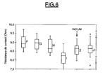
- the contact resistance of the devices was also measured Examples 1 and 2 and Comparative Examples A to J. The results are given in the graphs of Figures 5 and 6. These figures show that in in the case of PMOS devices, the contact resistance of the Example 2 is comparable to that of a standard device and slightly greater than that of the best device with an implantation arsenic. However, in the case of the NMOS device, the Example 1 according to the invention exhibits a much contact resistance weaker than the devices in the comparative examples, standard E and with implantation of arsenic A to D.
- a device 3 was manufactured by the method according to the invention and a device K by a standard method without implantation, as previously, but by performing a step of doping polysilicon by implantation of phosphorus atoms at a dose of 4.10 15 atoms per cm 2 at 25keV
- the prepopulated device K obtained by the standard process has an increased resistance compared to an E device ( Figure 2) obtained by the standard process but without additional doping with phosphorus.
- device 3 obtained by the process of the invention and with the additional doping with phosphorus presents a surface resistance still significantly lower than device E.
- a 40nm layer of titanium and a 25nm layer of titanium nitride were deposited on monocrystalline silicon wafers. Some of the wafers (identified by In) had undergone prior to deposition an indium implantation according to the invention at an implantation energy of 25 keV and an implantation rate of 10 14 atoms / cm 2 . Other sections (identified by the indication Ref.) Have not been subjected to the implantation of indium. The slices obtained were then subjected to rapid thermal annealing at different temperatures. The surface resistance of the titanium silicide obtained was measured.
- the formation of silicide is carried out at temperatures which can be 50 ° C lower than those necessary to obtain the desired surface resistance when the wafer has not been subjected to an indium implantation step.
Landscapes
- Electrodes Of Semiconductors (AREA)
- Insulated Gate Type Field-Effect Transistor (AREA)
- Metal-Oxide And Bipolar Metal-Oxide Semiconductor Integrated Circuits (AREA)
Applications Claiming Priority (2)
| Application Number | Priority Date | Filing Date | Title |
|---|---|---|---|
| FR9803134 | 1998-03-13 | ||
| FR9803134 | 1998-03-13 |
Publications (1)
| Publication Number | Publication Date |
|---|---|
| EP0942460A1 true EP0942460A1 (de) | 1999-09-15 |
Family
ID=9524037
Family Applications (1)
| Application Number | Title | Priority Date | Filing Date |
|---|---|---|---|
| EP99400584A Withdrawn EP0942460A1 (de) | 1998-03-13 | 1999-03-10 | Verfahren zur Herstellung einer Titansilizidschicht mit niedrigem Widerstand auf einem Halbleitersubstrat, und dadurch hergestellte Anordnung |
Country Status (3)
| Country | Link |
|---|---|
| US (2) | US6281556B1 (de) |
| EP (1) | EP0942460A1 (de) |
| JP (1) | JPH11297637A (de) |
Families Citing this family (14)
| Publication number | Priority date | Publication date | Assignee | Title |
|---|---|---|---|---|
| US6265297B1 (en) * | 1999-09-01 | 2001-07-24 | Micron Technology, Inc. | Ammonia passivation of metal gate electrodes to inhibit oxidation of metal |
| JP2001308027A (ja) * | 2000-04-25 | 2001-11-02 | Sharp Corp | 半導体装置の製造方法 |
| US6630385B1 (en) * | 2001-04-27 | 2003-10-07 | Advanced Micro Devices, Inc. | MOSFET with differential halo implant and annealing strategy |
| KR100402428B1 (ko) | 2001-12-18 | 2003-10-17 | 주식회사 하이닉스반도체 | 반도체 소자의 금속 배선 형성 방법 |
| US6682955B2 (en) * | 2002-05-08 | 2004-01-27 | Micron Technology, Inc. | Stacked die module and techniques for forming a stacked die module |
| JP2005005510A (ja) * | 2003-06-12 | 2005-01-06 | Toshiba Corp | 半導体装置及びその製造方法 |
| EP1489647A3 (de) * | 2003-06-20 | 2007-08-29 | STMicroelectronics S.A. | Herstellungsverfahren eines Silizids |
| FR2856514A1 (fr) * | 2003-06-20 | 2004-12-24 | St Microelectronics Sa | Procede de formation selective de siliciure sur une plaque de materiau semi-conducteur |
| TWI220792B (en) * | 2003-09-23 | 2004-09-01 | Promos Technologies Inc | Method for fabricating P-type gate NMOS transistor |
| BE1015721A3 (nl) * | 2003-10-17 | 2005-07-05 | Imec Inter Uni Micro Electr | Werkwijze voor het reduceren van de contactweerstand van de aansluitgebieden van een halfgeleiderinrichting. |
| JP4291197B2 (ja) | 2004-04-06 | 2009-07-08 | エルピーダメモリ株式会社 | 半導体装置及びその製造方法 |
| US20050266654A1 (en) * | 2004-05-27 | 2005-12-01 | Hattendorf Michael L | Barrier to amorphization implant |
| JP4237161B2 (ja) * | 2005-05-09 | 2009-03-11 | エルピーダメモリ株式会社 | 半導体装置の製造方法 |
| KR100685904B1 (ko) * | 2005-10-04 | 2007-02-26 | 동부일렉트로닉스 주식회사 | 풀리 실리사이드 게이트 및 그것을 가진 반도체 소자의제조 방법 |
Citations (5)
| Publication number | Priority date | Publication date | Assignee | Title |
|---|---|---|---|---|
| JPH05218069A (ja) * | 1992-02-07 | 1993-08-27 | Sharp Corp | Mosトランジスタおよびその製造方法 |
| US5545574A (en) * | 1995-05-19 | 1996-08-13 | Motorola, Inc. | Process for forming a semiconductor device having a metal-semiconductor compound |
| EP0746012A2 (de) * | 1995-06-02 | 1996-12-04 | Texas Instruments Incorporated | Verbesserungen bezüglich Silizidbildung |
| US5659194A (en) * | 1994-01-28 | 1997-08-19 | Mitsubishi Denki Kabushiki Kaisha | Semiconductor device having metal silicide film |
| EP0812009A2 (de) * | 1996-06-03 | 1997-12-10 | Texas Instruments Incorporated | Verbesserungen in der oder in Bezug auf die Halbleiterherstellung |
Family Cites Families (10)
| Publication number | Priority date | Publication date | Assignee | Title |
|---|---|---|---|---|
| AU570439B2 (en) | 1983-03-28 | 1988-03-17 | Compression Labs, Inc. | A combined intraframe and interframe transform coding system |
| US4821085A (en) * | 1985-05-01 | 1989-04-11 | Texas Instruments Incorporated | VLSI local interconnect structure |
| US4849802A (en) * | 1986-01-21 | 1989-07-18 | Ibm Corporation | Thermally stable low resistance contact |
| US5633202A (en) * | 1994-09-30 | 1997-05-27 | Intel Corporation | High tensile nitride layer |
| JPH08203842A (ja) * | 1995-01-30 | 1996-08-09 | Sony Corp | 半導体装置の製造方法 |
| JP3714995B2 (ja) * | 1995-07-05 | 2005-11-09 | シャープ株式会社 | 半導体装置 |
| US5960319A (en) * | 1995-10-04 | 1999-09-28 | Sharp Kabushiki Kaisha | Fabrication method for a semiconductor device |
| US6010952A (en) * | 1997-01-23 | 2000-01-04 | Lsi Logic Corporation | Process for forming metal silicide contacts using amorphization of exposed silicon while minimizing device degradation |
| US5985727A (en) * | 1997-06-30 | 1999-11-16 | Sun Microsystems, Inc. | Method for forming MOS devices with retrograde pocket regions and counter dopant regions buried in the substrate surface |
| US6146934A (en) * | 1997-12-19 | 2000-11-14 | Advanced Micro Devices, Inc. | Semiconductor device with asymmetric PMOS source/drain implant and method of manufacture thereof |
-
1999
- 1999-03-10 EP EP99400584A patent/EP0942460A1/de not_active Withdrawn
- 1999-03-11 JP JP11064813A patent/JPH11297637A/ja active Pending
- 1999-03-12 US US09/267,308 patent/US6281556B1/en not_active Expired - Fee Related
-
2001
- 2001-05-16 US US09/858,400 patent/US6812121B2/en not_active Expired - Lifetime
Patent Citations (5)
| Publication number | Priority date | Publication date | Assignee | Title |
|---|---|---|---|---|
| JPH05218069A (ja) * | 1992-02-07 | 1993-08-27 | Sharp Corp | Mosトランジスタおよびその製造方法 |
| US5659194A (en) * | 1994-01-28 | 1997-08-19 | Mitsubishi Denki Kabushiki Kaisha | Semiconductor device having metal silicide film |
| US5545574A (en) * | 1995-05-19 | 1996-08-13 | Motorola, Inc. | Process for forming a semiconductor device having a metal-semiconductor compound |
| EP0746012A2 (de) * | 1995-06-02 | 1996-12-04 | Texas Instruments Incorporated | Verbesserungen bezüglich Silizidbildung |
| EP0812009A2 (de) * | 1996-06-03 | 1997-12-10 | Texas Instruments Incorporated | Verbesserungen in der oder in Bezug auf die Halbleiterherstellung |
Non-Patent Citations (5)
| Title |
|---|
| ANONYMOUS: "Alloying of Tisi2.", IBM TECHNICAL DISCLOSURE BULLETIN, vol. 33, no. 7, December 1990 (1990-12-01), New York, US, pages 444, XP002107046 * |
| ANONYMOUS: "Doped Titanium Films for Salicide and Polycide", IBM TECHNICAL DISCLOSURE BULLETIN, vol. 28, no. 12, May 1986 (1986-05-01), New York, US, pages 5437 - 5438, XP002107047 * |
| HIROKI KUWANO ET AL: "RESISTIVITY AND MORPHOLOGY OF TISI2 FORMED ON XE+-IMPLANTED POLYCRYSTALLINE SILICON", APPLIED PHYSICS LETTERS, vol. 56, no. 5, 29 January 1990 (1990-01-29), pages 440 - 442, XP000128464 * |
| MOUROUX A ET AL: "Advances in the formation of C54-TiSi2 with an interposed refractory metal layer: some properties", MICROELECTRONIC ENGINEERING, vol. 37-38, November 1997 (1997-11-01), pages 449-454, XP004103516 * |
| PATENT ABSTRACTS OF JAPAN vol. 017, no. 657 (E - 1470) 6 December 1993 (1993-12-06) * |
Also Published As
| Publication number | Publication date |
|---|---|
| US6812121B2 (en) | 2004-11-02 |
| JPH11297637A (ja) | 1999-10-29 |
| US20030207569A1 (en) | 2003-11-06 |
| US6281556B1 (en) | 2001-08-28 |
Similar Documents
| Publication | Publication Date | Title |
|---|---|---|
| US5874342A (en) | Process for forming MOS device in integrated circuit structure using cobalt silicide contacts as implantation media | |
| JP2673104B2 (ja) | エピタキシャル・コバルト・シリサイド皮膜を形成する方法 | |
| US5633200A (en) | Process for manufacturing a large grain tungsten nitride film and process for manufacturing a lightly nitrided titanium salicide diffusion barrier with a large grain tungsten nitride cover layer | |
| US6281102B1 (en) | Cobalt silicide structure for improving gate oxide integrity and method for fabricating same | |
| KR0155587B1 (ko) | 반도체 웨이퍼의 실리콘 층 위에 규화 티탄 층을 형성하는 방법 | |
| US5739064A (en) | Second implanted matrix for agglomeration control and thermal stability | |
| US20080299720A1 (en) | STABILIZATION OF Ni MONOSILICIDE THIN FILMS IN CMOS DEVICES USING IMPLANTATION OF IONS BEFORE SILICIDATION | |
| US6187679B1 (en) | Low temperature formation of low resistivity titanium silicide | |
| WO2010033378A2 (en) | Method and apparatus for metal silicide formation | |
| CN100369219C (zh) | 使用Ni合金阻滞一硅化镍的结块作用 | |
| US6372566B1 (en) | Method of forming a silicide layer using metallic impurities and pre-amorphization | |
| US6812121B2 (en) | Process for forming a low resistivity titanium silicide layer on a silicon semiconductor substrate | |
| US20070037373A1 (en) | Salicide process utilizing a cluster ion implantation process | |
| US8586463B2 (en) | Method for preparing a layer comprising nickel monosilicide NiSi on a substrate comprising silicon | |
| US6479381B2 (en) | Process for forming a diffusion-barrier-material nitride film | |
| US20100013029A1 (en) | Structure and a Method of Manufacture for Low Resistance NiSix | |
| US20100164001A1 (en) | Implant process for blocked salicide poly resistor and structures formed thereby | |
| US20070167009A1 (en) | Method of fabricating nickel silicide | |
| KR20050015108A (ko) | 반도체 소자 제조방법 및 이에 의하여 제조된 반도체 소자 | |
| US7622386B2 (en) | Method for improved formation of nickel silicide contacts in semiconductor devices | |
| KR100325302B1 (ko) | 반도체 소자의 제조방법 | |
| KR100270185B1 (ko) | 저저항 티타늄 실리사이드 층 형성 방법 및 그를 포함하는 반도체 디바이스 | |
| Ishigami et al. | Ti Salicide Technology using Nitrogen Diffusion from Tin Cap by RTA in an Argon Ambient | |
| FR2892856A1 (fr) | Formation de zones de siliciure dans un dispositif semiconducteur | |
| Tanaka et al. | Issues for Pd2Si and NiSi Fully Silicided Gate Formation |
Legal Events
| Date | Code | Title | Description |
|---|---|---|---|
| PUAI | Public reference made under article 153(3) epc to a published international application that has entered the european phase |
Free format text: ORIGINAL CODE: 0009012 |
|
| AK | Designated contracting states |
Kind code of ref document: A1 Designated state(s): DE FR GB IT |
|
| AX | Request for extension of the european patent |
Free format text: AL;LT;LV;MK;RO;SI |
|
| 17P | Request for examination filed |
Effective date: 19990914 |
|
| AKX | Designation fees paid |
Free format text: DE FR GB IT |
|
| RAP1 | Party data changed (applicant data changed or rights of an application transferred) |
Owner name: FRANCE TELECOM Owner name: KONINKLIJKE PHILIPS ELECTRONICS N.V. Owner name: STMICROELECTRONICS S.A. |
|
| 17Q | First examination report despatched |
Effective date: 20071026 |
|
| RAP1 | Party data changed (applicant data changed or rights of an application transferred) |
Owner name: FRANCE TELECOM Owner name: NXP B.V. Owner name: STMICROELECTRONICS S.A. |
|
| STAA | Information on the status of an ep patent application or granted ep patent |
Free format text: STATUS: THE APPLICATION IS DEEMED TO BE WITHDRAWN |
|
| 18D | Application deemed to be withdrawn |
Effective date: 20091001 |