EP0942467A1 - Procédé de fabrication des dispositifs bipolaires et BiCMOS - Google Patents
Procédé de fabrication des dispositifs bipolaires et BiCMOS Download PDFInfo
- Publication number
- EP0942467A1 EP0942467A1 EP99301543A EP99301543A EP0942467A1 EP 0942467 A1 EP0942467 A1 EP 0942467A1 EP 99301543 A EP99301543 A EP 99301543A EP 99301543 A EP99301543 A EP 99301543A EP 0942467 A1 EP0942467 A1 EP 0942467A1
- Authority
- EP
- European Patent Office
- Prior art keywords
- gap
- layer
- silicon
- window
- oxide
- Prior art date
- Legal status (The legal status is an assumption and is not a legal conclusion. Google has not performed a legal analysis and makes no representation as to the accuracy of the status listed.)
- Granted
Links
- 238000000034 method Methods 0.000 title claims abstract description 33
- 229910052710 silicon Inorganic materials 0.000 claims abstract description 46
- 239000010703 silicon Substances 0.000 claims abstract description 46
- XUIMIQQOPSSXEZ-UHFFFAOYSA-N Silicon Chemical compound [Si] XUIMIQQOPSSXEZ-UHFFFAOYSA-N 0.000 claims abstract description 45
- 239000000758 substrate Substances 0.000 claims abstract description 31
- 229910021420 polycrystalline silicon Inorganic materials 0.000 claims abstract description 29
- 239000000463 material Substances 0.000 claims abstract description 9
- 238000004519 manufacturing process Methods 0.000 claims abstract description 5
- 229910021417 amorphous silicon Inorganic materials 0.000 claims abstract description 4
- 238000004518 low pressure chemical vapour deposition Methods 0.000 claims description 9
- QVGXLLKOCUKJST-UHFFFAOYSA-N atomic oxygen Chemical compound [O] QVGXLLKOCUKJST-UHFFFAOYSA-N 0.000 claims description 3
- 229910052760 oxygen Inorganic materials 0.000 claims description 3
- 239000001301 oxygen Substances 0.000 claims description 3
- 238000005229 chemical vapour deposition Methods 0.000 claims description 2
- 239000000126 substance Substances 0.000 claims description 2
- VYPSYNLAJGMNEJ-UHFFFAOYSA-N Silicium dioxide Chemical compound O=[Si]=O VYPSYNLAJGMNEJ-UHFFFAOYSA-N 0.000 claims 2
- 235000012239 silicon dioxide Nutrition 0.000 claims 1
- 239000000377 silicon dioxide Substances 0.000 claims 1
- 229920005591 polysilicon Polymers 0.000 abstract description 26
- 230000015572 biosynthetic process Effects 0.000 abstract description 4
- 230000003647 oxidation Effects 0.000 description 10
- 238000007254 oxidation reaction Methods 0.000 description 10
- ZOXJGFHDIHLPTG-UHFFFAOYSA-N Boron Chemical compound [B] ZOXJGFHDIHLPTG-UHFFFAOYSA-N 0.000 description 5
- 239000012080 ambient air Substances 0.000 description 5
- 229910052796 boron Inorganic materials 0.000 description 5
- 239000000243 solution Substances 0.000 description 5
- 238000005468 ion implantation Methods 0.000 description 4
- 238000004458 analytical method Methods 0.000 description 3
- 238000002513 implantation Methods 0.000 description 3
- 230000005641 tunneling Effects 0.000 description 3
- KRHYYFGTRYWZRS-UHFFFAOYSA-N Fluorane Chemical compound F KRHYYFGTRYWZRS-UHFFFAOYSA-N 0.000 description 2
- 229910052581 Si3N4 Inorganic materials 0.000 description 2
- 238000000151 deposition Methods 0.000 description 2
- 230000008021 deposition Effects 0.000 description 2
- 238000005516 engineering process Methods 0.000 description 2
- 238000005530 etching Methods 0.000 description 2
- BHEPBYXIRTUNPN-UHFFFAOYSA-N hydridophosphorus(.) (triplet) Chemical compound [PH] BHEPBYXIRTUNPN-UHFFFAOYSA-N 0.000 description 2
- 230000010354 integration Effects 0.000 description 2
- 239000004065 semiconductor Substances 0.000 description 2
- HQVNEWCFYHHQES-UHFFFAOYSA-N silicon nitride Chemical compound N12[Si]34N5[Si]62N3[Si]51N64 HQVNEWCFYHHQES-UHFFFAOYSA-N 0.000 description 2
- OAICVXFJPJFONN-UHFFFAOYSA-N Phosphorus Chemical compound [P] OAICVXFJPJFONN-UHFFFAOYSA-N 0.000 description 1
- BLRPTPMANUNPDV-UHFFFAOYSA-N Silane Chemical compound [SiH4] BLRPTPMANUNPDV-UHFFFAOYSA-N 0.000 description 1
- BOTDANWDWHJENH-UHFFFAOYSA-N Tetraethyl orthosilicate Chemical compound CCO[Si](OCC)(OCC)OCC BOTDANWDWHJENH-UHFFFAOYSA-N 0.000 description 1
- 230000002411 adverse Effects 0.000 description 1
- 239000003570 air Substances 0.000 description 1
- 238000000137 annealing Methods 0.000 description 1
- 239000006117 anti-reflective coating Substances 0.000 description 1
- 239000007864 aqueous solution Substances 0.000 description 1
- 229910052785 arsenic Inorganic materials 0.000 description 1
- RQNWIZPPADIBDY-UHFFFAOYSA-N arsenic atom Chemical compound [As] RQNWIZPPADIBDY-UHFFFAOYSA-N 0.000 description 1
- 238000004891 communication Methods 0.000 description 1
- 238000007796 conventional method Methods 0.000 description 1
- 238000010586 diagram Methods 0.000 description 1
- 238000009792 diffusion process Methods 0.000 description 1
- 239000002019 doping agent Substances 0.000 description 1
- 230000000694 effects Effects 0.000 description 1
- 230000003028 elevating effect Effects 0.000 description 1
- 239000007943 implant Substances 0.000 description 1
- 238000002955 isolation Methods 0.000 description 1
- 230000000873 masking effect Effects 0.000 description 1
- 230000035515 penetration Effects 0.000 description 1
- 229910052698 phosphorus Inorganic materials 0.000 description 1
- 239000011574 phosphorus Substances 0.000 description 1
- 229910000077 silane Inorganic materials 0.000 description 1
- 150000003376 silicon Chemical class 0.000 description 1
- 125000006850 spacer group Chemical group 0.000 description 1
- WQJQOUPTWCFRMM-UHFFFAOYSA-N tungsten disilicide Chemical compound [Si]#[W]#[Si] WQJQOUPTWCFRMM-UHFFFAOYSA-N 0.000 description 1
- 229910021342 tungsten silicide Inorganic materials 0.000 description 1
- 238000000038 ultrahigh vacuum chemical vapour deposition Methods 0.000 description 1
Images

Classifications
-
- H—ELECTRICITY
- H10—SEMICONDUCTOR DEVICES; ELECTRIC SOLID-STATE DEVICES NOT OTHERWISE PROVIDED FOR
- H10D—INORGANIC ELECTRIC SEMICONDUCTOR DEVICES
- H10D84/00—Integrated devices formed in or on semiconductor substrates that comprise only semiconducting layers, e.g. on Si wafers or on GaAs-on-Si wafers
- H10D84/01—Manufacture or treatment
- H10D84/0107—Integrating at least one component covered by H10D12/00 or H10D30/00 with at least one component covered by H10D8/00, H10D10/00 or H10D18/00, e.g. integrating IGFETs with BJTs
- H10D84/0109—Integrating at least one component covered by H10D12/00 or H10D30/00 with at least one component covered by H10D8/00, H10D10/00 or H10D18/00, e.g. integrating IGFETs with BJTs the at least one component covered by H10D12/00 or H10D30/00 being a MOS device
-
- H—ELECTRICITY
- H10—SEMICONDUCTOR DEVICES; ELECTRIC SOLID-STATE DEVICES NOT OTHERWISE PROVIDED FOR
- H10D—INORGANIC ELECTRIC SEMICONDUCTOR DEVICES
- H10D84/00—Integrated devices formed in or on semiconductor substrates that comprise only semiconducting layers, e.g. on Si wafers or on GaAs-on-Si wafers
- H10D84/01—Manufacture or treatment
- H10D84/02—Manufacture or treatment characterised by using material-based technologies
- H10D84/03—Manufacture or treatment characterised by using material-based technologies using Group IV technology, e.g. silicon technology or silicon-carbide [SiC] technology
- H10D84/038—Manufacture or treatment characterised by using material-based technologies using Group IV technology, e.g. silicon technology or silicon-carbide [SiC] technology using silicon technology, e.g. SiGe
-
- H—ELECTRICITY
- H10—SEMICONDUCTOR DEVICES; ELECTRIC SOLID-STATE DEVICES NOT OTHERWISE PROVIDED FOR
- H10D—INORGANIC ELECTRIC SEMICONDUCTOR DEVICES
- H10D84/00—Integrated devices formed in or on semiconductor substrates that comprise only semiconducting layers, e.g. on Si wafers or on GaAs-on-Si wafers
- H10D84/40—Integrated devices formed in or on semiconductor substrates that comprise only semiconducting layers, e.g. on Si wafers or on GaAs-on-Si wafers characterised by the integration of at least one component covered by groups H10D12/00 or H10D30/00 with at least one component covered by groups H10D10/00 or H10D18/00, e.g. integration of IGFETs with BJTs
- H10D84/401—Combinations of FETs or IGBTs with BJTs
Definitions
- the invention is directed to a process for semiconductor devices and in particular to processes for making bipolar and metal-oxide-semiconductor (MOS) devices (BiCMOS devices) on a single silicon substrate.
- MOS metal-oxide-semiconductor
- Kinoshita et al. describe an integrated process for forming a bipolar device and an MOS device on a substrate.
- the integrate process utilizes a heavily doped epitaxial layer to both connect the base polysilicon electrode to the n-epi (collector) surface and as the diffusion source to form a bipolar graft base.
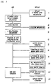
- the process described in Kinoshita is illustrated in the process flow sequence provided in FIG. 1.
- FIG. 1 illustrates the integrated steps for producing an MOS device and a bipolar device on a single substrate.
- step 10 an n + buried layer is formed in a silicon substrate.
- a p + buried layer is formed by high energy ion implantation followed by p-well and n-channel implantation.
- LOCOS localized oxidation of silicon isolation is performed in step 30, during which field oxide regions are formed on the silicon substrate.
- the collector plug is formed by phosphorous ion implantation.
- N-well and p-channel implantations are performed in step 50, followed by the formation of a thin layer (7 nm thickness) of gate oxide, doped (boron for the bipolar device and either boron or arsenic or phosphorus for the MOS device) polysilicon (150 nm thickness) and silicon nitride layers (200 nm thickness) in step 60.
- the doped, polysilicon layer is the gate electrode of the MOS device and the base electrodes of the bipolar transistors.
- step 70 an emitter opening is formed and the gate oxide is removed from the bottom of the emitter opening using a wet etch. In this step a gap is formed under the undoped polysilicon layer.
- step 80 heavily boron-doped epitaxial layer is then formed on the surface of the substrate using an ultra high vacuum chemical vapor deposition.
- step 90 the heavily boron doped layer is selectively removed, leaving only that portion of the layer at the base of the emitter window.
- step 100 a BF 2 ion implantation is used to form the intrinsic base, followed by a phosphorous implantation for forming the selective ion-implanted collector (SIC) and oxide spacer formation.
- step 110 the bipolar base electrode and MOS gate are formed simultaneously.
- step 120 a furnace anneal was performed for bipolar emitter and extrinsic base drive-in. This annealing step also activates the source/drain and gate electrodes of the nMOS device.
- the gap underlying the undoped silicon layer is difficult to fill when the size of the gap is less than 200 nm using chemical vapor deposition, because of the gaps that form in the fill as the fill material builds up on the bottom and top of the gap.
- Current CMOS technology requires gate oxide thicknesses of about 1.5 nm to about 6 nm. Since the gap results from the removal of the gate oxide, gap sizes are also in the range of about 1.5 nm to about 6 nm. As previously noted, gaps of this size are difficult to fill uniformly. Because a less than completely filled gap will cause problems in device performance, a process in which these gaps are completely filled in is desired.
- the present invention is directed to a process for device fabrication in which a gap is formed between two layers which are no more than 200 nm apart and then subsequently filled.
- a thin gate oxide layer i.e. an oxide layer with a thickness of 200 nm or less
- the fabrication of the bipolar device requires the removal of the gate oxide under the extrinsic base region in order to fabricate the extrinsic base.
- the gate oxide under the extrinsic base is removed after the emitter opening is formed in the extrinsic base silicon.
- the process steps are performed in this sequence in order to obtain a desirable and efficient integration of the process for fabricating the CMOS device and the process for fabricating the bipolar device.
- a gap is formed under the extrinsic base silicon (typically the extrinsic base silicon is amorphous when the gap is formed and refilled and, afterwards, the amorphous silicon is annealed to form polysilicon, for convenience herein, this silicon layer is referred to as the extrinsic base silicon) which is subsequently refilled with doped silicon.
- the gap is formed not only by removing the gate oxide underlying the extrinsic base silicon, but by etching a portion of the underlying silicon and the overlying extrinsic base silicon in a manner that provides a gap wherein the distance between the underlying silicon and the overlying extrinsic base silicon is greater at the gap opening into the emitter opening than at the end of the gap adjacent to the remaining gate oxide.
- the gap opening is referred to as the proximate end of the gap and the gap end is referred to as the distal end of the gap.
- the distance between the underlying silicon and the overlying extrinsic base silicon is equal to the thickness of the gate oxide at the distal end of the gap and greater than the thickness of the gate oxide at the proximate end of the gap. Therefore, after the gate oxide is removed and the gap is formed, the underlying silicon and the overlying extrinsic base silicon are subjected to conditions that cause their removal at the proximate end of the gap at a rate faster than their rate of removal at the distal end of the gap.
- the gap is subjected to conditions that cause the underlying silicon and the overlying extrinsic base silicon to oxidize. Because of the nature of the gap, the underlying silicon and the overlying extrinsic base silicon at the proximate end of the gap oxidize at a faster rate than the overlying extrinsic base silicon and the underlying silicon at the distal end of the gap. Conventional expedients are employed to achieve the desired taper in the gap. It is advantageous if the gap is subjected to conditions that oxidize the overlying polysilicon and underlying silicon.
- a combination of conventional oxidation expedients such as controlled furnace oxidation, chemical oxidation, or by subjecting the gap to an oxygen containing atmosphere at ambient temperature are contemplated as suitable. After the oxide is formed, it is removed using conventional expedients for the removal of oxide such as an aqueous solution of hydrofluoric acid.
- a tapered gap is one in which the distance between the overlying extrinsic base silicon and the underlying base silicon changes gradually from the first distance at the proximate end to the gap to the second distance at the distal end of the gap.
- the gap is subjected to the conditions for a sufficient amount of time to achieve the desired configuration.
- the desired degree of taper is a function of the thickness of the gate oxide layer that was removed to form the gap. It is advantageous if, after the gap is formed, it is subjected to conditions that provide a first distance at the proximate end of the gap that is at least ten percent greater than the second distance at the distal end of the gap. The resulting gap is then refilled with polysilicon using a conventional technique such as low pressure chemical vapor deposition. Low pressure chemical vapor deposition is easier and less expensive than the deposition of amorphous silicon using ultra high vacuum.
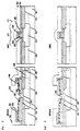
- FIG. 2 illustrates a substrate 305 on which a bipolar device 310 and a CMOS device 315 are being simultaneously formed.
- a buried layer region 316 is formed in the substrate 305 by ion implantation followed by an oxidation step to drive the dopants into the substrate 305.
- N-well regions 325, p-well region 320, and field oxide region 335 are formed on the substrate 305.
- a reach through implant (also referred to as a sinker) 340 is also formed in the substrate 305.
- a gate oxide 330 is formed on the substrate 305.
- the gate oxide has a thickness in the range of about 2 nm to about 20 nm. For CMOS devices made according to 0.25 ⁇ m device rules, the thickness of the gate oxide is about 4.5 nm. For CMOS devices made according to 0.18 ⁇ m device rules, the thickness of the gate oxide is about 2.5 nm.
- Layers of polysilicon 345, tungsten silicide 346, silicon nitride 350, plasma enhanced tetraethylorthosilicate (PETEOS) 355 and an anti-reflective coating 360 were sequentially formed on the substrate 305.
- the emitter opening 365 and the gate 370 were defined simultaneously by selective removal of portions of layers 345, 350, 355, and 360.
- Layers of PETEOS 361 and a polysilicon hardmask 362 were then deposited and patterned.
- the substrate was then subjected to conditions that removed the gate oxide 330 from the bottom of the emitter opening 365.
- a portion of the gate oxide 330 underlying the polysilicon is 345 is also removed by this step to form the gap 375.
- Suitable expedients include exposing the gap 375 to an oxygen-containing atmosphere such as ambient air for a period of time that is sufficient to oxidize a portion of the extrinsic base silicon and the underlying silicon to the desired extent.
- Suitable conditions are capable of wide variation depending upon the desired degree of oxidation. If the extrinsic base silicon and the underlying silicon are oxidized in ambient air (i.e. air at a temperature of about 30°C) the time required to obtain the desired degree of oxidation could vary from about 24 hours to about 30 days.
- the objective of this step is to introduce a tapered gap that is wider at its proximate end 380 than it is at its distal end 385.
- the gap is subjected to the oxidation expedient for a time sufficient to increase the gap height 375 at its proximate end 380 by at least about ten percent over the gap height at the distal end 385.
- polysilicon 390 is deposited over the surface of the substrate 305. Because of the tapered gap 375, the polysilicon 390 does not have gaps therein which could adversely affect the contact between the extrinsic base and the intrinsic base and the bipolar device 310.
- an emitter opening with a 20 nm thick layer of oxide at the base thereof.
- the gate oxide in the emitter opening was removed using a 100:1 solution of aqueous HF for 70 minutes.
- the substrate was then rinsed and dried using conventional expedients.
- the substrate was then stored in ambient air for about 24 hours.
- the gap was then filled with polysilicon using a low pressure chemical vapor deposition system (LPCVD).
- LPCVD low pressure chemical vapor deposition system
- the LPCVD tool was obtained from SemiTherm of Kalispell, Montana. The tool was designed to perform vertically oriented low pressure chemical vapor deposition.
- the deposition occurred at a temperature of 550°C, a pressure of 250 mTorr, and with a silane flow of about 40 sccm through a first (top) injector and about 70 sccm through a second (bottom) injector.
- the growth rate of the polysilicon was about 2nm/minute.
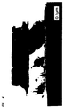
- the resulting structure was subjected to a TEM (tunneling electron microscope) analysis.
- the gap height is essentially constant from the proximate end to the distal end of the gap.
- the gap is not uniformly filled with the polysilicon, as evidenced by the light regions in the approximated center of the layer of polysilicon.
- an emitter opening With a 6 nm thick layer of oxide at the base thereof.
- the gate oxide in the emitter opening was removed using a 100:1 solution of aqueous HF for 70 minutes.
- the substrate was then rinsed and dried using conventional expedients.
- the substrate was then stored in ambient air for about 24 hours.
- the oxide was then removed using a 100:1 solution of aqueous HF for 1 minute.
- the gap was then filled with polysilicon using a low pressure chemical vapor deposition system using the previously described tools and conditions.
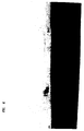
- the gap height has a different height at the proximate end thereof than at the distal end thereof.
- the height of the gap at the proximate end is clearly greater than the height of the gap at the distal end. Furthermore, there are no light regions in the layer of polysilicon so formed, which indicates that the polysilicon uniformly filled the gap.
- an emitter opening with a 2.5 nm thick layer of oxide at the base thereof.
- the gate oxide in the emitter opening was removed using a 100:1 solution of aqueous HF for 70 minutes.
- the lateral etch of the oxide proceeded about 60 nm under the polysilicon.
- the substrate was then rinsed and dried using conventional expedients.
- the substrate was then stored in ambient air for about 30 days.
- An aqueous HF solution (100:1) was used to remove the oxide.
- the gap was then filled with polysilicon using a low pressure chemical vapor deposition system as described in the previous example.
- the gap height is greater at the proximate end of the gap than at the distal end of the gap.
- the gap height also changes gradually from the proximate end to the distal end of the gap.
- the gap is uniformly filled with the polysilicon, as evidenced by the uniform appearance of the layer of polysilicon.
Landscapes
- Metal-Oxide And Bipolar Metal-Oxide Semiconductor Integrated Circuits (AREA)
- Bipolar Transistors (AREA)
- Bipolar Integrated Circuits (AREA)
Applications Claiming Priority (2)
| Application Number | Priority Date | Filing Date | Title |
|---|---|---|---|
| US09/042,388 US6121101A (en) | 1998-03-12 | 1998-03-12 | Process for fabricating bipolar and BiCMOS devices |
| US42388 | 1998-03-12 |
Publications (2)
| Publication Number | Publication Date |
|---|---|
| EP0942467A1 true EP0942467A1 (fr) | 1999-09-15 |
| EP0942467B1 EP0942467B1 (fr) | 2000-11-15 |
Family
ID=21921656
Family Applications (1)
| Application Number | Title | Priority Date | Filing Date |
|---|---|---|---|
| EP99301543A Expired - Lifetime EP0942467B1 (fr) | 1998-03-12 | 1999-03-02 | Procédé de fabrication des dispositifs bipolaires et BiCMOS |
Country Status (5)
| Country | Link |
|---|---|
| US (1) | US6121101A (fr) |
| EP (1) | EP0942467B1 (fr) |
| JP (1) | JP3328600B2 (fr) |
| KR (1) | KR100549974B1 (fr) |
| DE (1) | DE69900028T2 (fr) |
Cited By (1)
| Publication number | Priority date | Publication date | Assignee | Title |
|---|---|---|---|---|
| DE102004053394A1 (de) * | 2004-11-05 | 2006-05-11 | Atmel Germany Gmbh | Halbleiteranordnung und Verfahren zur Herstellung einer Halbleiteranordnung |
Families Citing this family (4)
| Publication number | Priority date | Publication date | Assignee | Title |
|---|---|---|---|---|
| KR100486112B1 (ko) * | 2002-08-02 | 2005-04-29 | 매그나칩 반도체 유한회사 | 바이 씨 모스 트랜지스터의 제조방법 |
| US6960820B2 (en) * | 2003-07-01 | 2005-11-01 | International Business Machines Corporation | Bipolar transistor self-alignment with raised extrinsic base extension and methods of forming same |
| US7002221B2 (en) * | 2003-08-29 | 2006-02-21 | International Business Machines Corporation | Bipolar transistor having raised extrinsic base with selectable self-alignment and methods of forming same |
| US8716096B2 (en) | 2011-12-13 | 2014-05-06 | International Business Machines Corporation | Self-aligned emitter-base in advanced BiCMOS technology |
Citations (3)
| Publication number | Priority date | Publication date | Assignee | Title |
|---|---|---|---|---|
| DE3940394A1 (de) * | 1988-12-06 | 1990-06-07 | Kabushiki Kaisha Toshiba, Kawasaki, Kanagawa | Verfahren zum herstellen einer halbleitervorrichtung |
| EP0435257A2 (fr) * | 1989-12-27 | 1991-07-03 | Oki Electric Industry Co., Ltd. | Procédé de fabrication d'un dispositif semi-conducteur biMOS à fiabilité et rapidité améliorées |
| US5648279A (en) * | 1994-06-21 | 1997-07-15 | Nec Corporation | Method of manufacturing bipolar transistor having emitter region and external base region formed in self alignment manner |
Family Cites Families (5)
| Publication number | Priority date | Publication date | Assignee | Title |
|---|---|---|---|---|
| JP3156436B2 (ja) * | 1993-04-05 | 2001-04-16 | 日本電気株式会社 | ヘテロ接合バイポーラトランジスタ |
| JP2630237B2 (ja) * | 1993-12-22 | 1997-07-16 | 日本電気株式会社 | 半導体装置及びその製造方法 |
| US5620908A (en) * | 1994-09-19 | 1997-04-15 | Kabushiki Kaisha Toshiba | Manufacturing method of semiconductor device comprising BiCMOS transistor |
| WO1997015071A1 (fr) * | 1995-10-20 | 1997-04-24 | Philips Electronics N.V. | Fabrication d'un dispositif semi-conducteur avec une zone semi-conductrice deposee selectivement |
| US5773350A (en) * | 1997-01-28 | 1998-06-30 | National Semiconductor Corporation | Method for forming a self-aligned bipolar junction transistor with silicide extrinsic base contacts and selective epitaxial grown intrinsic base |
-
1998
- 1998-03-12 US US09/042,388 patent/US6121101A/en not_active Expired - Lifetime
-
1999
- 1999-03-02 EP EP99301543A patent/EP0942467B1/fr not_active Expired - Lifetime
- 1999-03-02 DE DE69900028T patent/DE69900028T2/de not_active Expired - Lifetime
- 1999-03-11 KR KR1019990008029A patent/KR100549974B1/ko not_active Expired - Fee Related
- 1999-03-12 JP JP06574099A patent/JP3328600B2/ja not_active Expired - Fee Related
Patent Citations (3)
| Publication number | Priority date | Publication date | Assignee | Title |
|---|---|---|---|---|
| DE3940394A1 (de) * | 1988-12-06 | 1990-06-07 | Kabushiki Kaisha Toshiba, Kawasaki, Kanagawa | Verfahren zum herstellen einer halbleitervorrichtung |
| EP0435257A2 (fr) * | 1989-12-27 | 1991-07-03 | Oki Electric Industry Co., Ltd. | Procédé de fabrication d'un dispositif semi-conducteur biMOS à fiabilité et rapidité améliorées |
| US5648279A (en) * | 1994-06-21 | 1997-07-15 | Nec Corporation | Method of manufacturing bipolar transistor having emitter region and external base region formed in self alignment manner |
Non-Patent Citations (2)
| Title |
|---|
| HIROKAZU FUJIMAKI: "HIGH SPEED SUB-HALF MICRON SATURN TRANSISTOR USING EPITAXIAL BASE TECHNOLOGY", IEICE TRANSACTIONS ON ELECTRONICS, vol. E76-C, no. 4, 1 April 1993 (1993-04-01), pages 577 - 581, XP000378319 * |
| KINOSHITA Y ET AL: "PROCESS INTEGRATION TECHNOLOGY FOR SUB-30PS ECL BICMOS USING HEAVILY BORON DOPED EPITAXIAL CONTACT (HYDEC)", TECHNICAL DIGEST OF THE INTERNATIONAL ELECTRON DEVICES MEETING, SAN FRANCISCO, DEC. 11 - 14, 1994, no. MEETING 40, 22 October 1995 (1995-10-22), INSTITUTE OF ELECTRICAL AND ELECTRONICS ENGINEERS, pages 441 - 444, XP000585528 * |
Cited By (3)
| Publication number | Priority date | Publication date | Assignee | Title |
|---|---|---|---|---|
| DE102004053394A1 (de) * | 2004-11-05 | 2006-05-11 | Atmel Germany Gmbh | Halbleiteranordnung und Verfahren zur Herstellung einer Halbleiteranordnung |
| US7601584B2 (en) | 2004-11-05 | 2009-10-13 | Atmel Germany Gmbh | Semiconductor array and method for manufacturing a semiconductor array |
| DE102004053394B4 (de) * | 2004-11-05 | 2010-08-19 | Atmel Automotive Gmbh | Halbleiteranordnung und Verfahren zur Herstellung einer Halbleiteranordnung |
Also Published As
| Publication number | Publication date |
|---|---|
| US6121101A (en) | 2000-09-19 |
| JPH11330281A (ja) | 1999-11-30 |
| DE69900028T2 (de) | 2001-03-22 |
| EP0942467B1 (fr) | 2000-11-15 |
| KR19990077768A (ko) | 1999-10-25 |
| KR100549974B1 (ko) | 2006-02-08 |
| DE69900028D1 (de) | 2000-12-21 |
| JP3328600B2 (ja) | 2002-09-24 |
Similar Documents
| Publication | Publication Date | Title |
|---|---|---|
| US5234850A (en) | Method of fabricating a nitride capped MOSFET for integrated circuits | |
| US5504031A (en) | Elevated source/drain with solid phase diffused source/drain extension for deep sub-micron mosfets | |
| US4784971A (en) | Process for manufacturing semiconductor BICMOS device | |
| JP2663402B2 (ja) | Cmos集積回路デバイスの製造方法 | |
| KR100400323B1 (ko) | 반도체 소자의 시모스(cmos) 및 그의 제조 방법 | |
| US5196367A (en) | Modified field isolation process with no channel-stop implant encroachment | |
| JPH0677421A (ja) | トランジスタの製法 | |
| US6087239A (en) | Disposable spacer and method of forming and using same | |
| EP0768709B1 (fr) | Procédé BiCMOS avec transistor bipolaire ayant un faible courant de recombinaison de base | |
| EP0518611B1 (fr) | Procédé de manufacture d'une structure semi-conductrice ayant des dispositifs MOS et bipolaires | |
| US5466615A (en) | Silicon damage free process for double poly emitter and reverse MOS in BiCMOS application | |
| JPH09232445A (ja) | 半導体装置およびその製造方法 | |
| US5286672A (en) | Method for forming field oxide regions | |
| JPH0727915B2 (ja) | 半導体装置の製造方法 | |
| KR100212101B1 (ko) | Mos 트랜지스터를 독립적으로 형성할 수 있는 반도체 접적회로 디바이스를 제조하기 위한 방법 | |
| US5879999A (en) | Method of manufacturing an insulated gate semiconductor device having a spacer extension | |
| US5057455A (en) | Formation of integrated circuit electrodes | |
| JPH0645343A (ja) | ボロシリケイトガラススペーサを有する半導体装置及びその製造方法 | |
| US6121101A (en) | Process for fabricating bipolar and BiCMOS devices | |
| US5115296A (en) | Preferential oxidization self-aligned contact technology | |
| US6445043B1 (en) | Isolated regions in an integrated circuit | |
| JPH05267331A (ja) | Mos型半導体装置の製造方法 | |
| EP0656660B1 (fr) | Procédé pour fabriquer des BiCMOS | |
| US5612247A (en) | Method for fabricating isolation region for a semiconductor device | |
| WO1984004853A1 (fr) | Procede de fabrication d'un dispositif a semi-conducteur |
Legal Events
| Date | Code | Title | Description |
|---|---|---|---|
| PUAI | Public reference made under article 153(3) epc to a published international application that has entered the european phase |
Free format text: ORIGINAL CODE: 0009012 |
|
| 17P | Request for examination filed |
Effective date: 19990317 |
|
| AK | Designated contracting states |
Kind code of ref document: A1 Designated state(s): DE FR GB |
|
| AX | Request for extension of the european patent |
Free format text: AL;LT;LV;MK;RO;SI |
|
| 17Q | First examination report despatched |
Effective date: 19990810 |
|
| GRAG | Despatch of communication of intention to grant |
Free format text: ORIGINAL CODE: EPIDOS AGRA |
|
| GRAG | Despatch of communication of intention to grant |
Free format text: ORIGINAL CODE: EPIDOS AGRA |
|
| GRAH | Despatch of communication of intention to grant a patent |
Free format text: ORIGINAL CODE: EPIDOS IGRA |
|
| AKX | Designation fees paid |
Free format text: DE FR GB |
|
| GRAH | Despatch of communication of intention to grant a patent |
Free format text: ORIGINAL CODE: EPIDOS IGRA |
|
| GRAA | (expected) grant |
Free format text: ORIGINAL CODE: 0009210 |
|
| AK | Designated contracting states |
Kind code of ref document: B1 Designated state(s): DE FR GB |
|
| ET | Fr: translation filed | ||
| REF | Corresponds to: |
Ref document number: 69900028 Country of ref document: DE Date of ref document: 20001221 |
|
| PLBE | No opposition filed within time limit |
Free format text: ORIGINAL CODE: 0009261 |
|
| STAA | Information on the status of an ep patent application or granted ep patent |
Free format text: STATUS: NO OPPOSITION FILED WITHIN TIME LIMIT |
|
| 26N | No opposition filed | ||
| REG | Reference to a national code |
Ref country code: GB Ref legal event code: IF02 |
|
| PGFP | Annual fee paid to national office [announced via postgrant information from national office to epo] |
Ref country code: FR Payment date: 20140311 Year of fee payment: 16 |
|
| REG | Reference to a national code |
Ref country code: FR Ref legal event code: ST Effective date: 20151130 |
|
| PG25 | Lapsed in a contracting state [announced via postgrant information from national office to epo] |
Ref country code: FR Free format text: LAPSE BECAUSE OF NON-PAYMENT OF DUE FEES Effective date: 20150331 |
|
| PGFP | Annual fee paid to national office [announced via postgrant information from national office to epo] |
Ref country code: DE Payment date: 20160218 Year of fee payment: 18 |
|
| PGFP | Annual fee paid to national office [announced via postgrant information from national office to epo] |
Ref country code: GB Payment date: 20160223 Year of fee payment: 18 |
|
| REG | Reference to a national code |
Ref country code: DE Ref legal event code: R119 Ref document number: 69900028 Country of ref document: DE |
|
| GBPC | Gb: european patent ceased through non-payment of renewal fee |
Effective date: 20170302 |
|
| PG25 | Lapsed in a contracting state [announced via postgrant information from national office to epo] |
Ref country code: DE Free format text: LAPSE BECAUSE OF NON-PAYMENT OF DUE FEES Effective date: 20171003 |
|
| PG25 | Lapsed in a contracting state [announced via postgrant information from national office to epo] |
Ref country code: GB Free format text: LAPSE BECAUSE OF NON-PAYMENT OF DUE FEES Effective date: 20170302 |