EP0942471A2 - Schaltung mit kleiner Packung für MOSFETS - Google Patents
Schaltung mit kleiner Packung für MOSFETS Download PDFInfo
- Publication number
- EP0942471A2 EP0942471A2 EP99301818A EP99301818A EP0942471A2 EP 0942471 A2 EP0942471 A2 EP 0942471A2 EP 99301818 A EP99301818 A EP 99301818A EP 99301818 A EP99301818 A EP 99301818A EP 0942471 A2 EP0942471 A2 EP 0942471A2
- Authority
- EP
- European Patent Office
- Prior art keywords
- mosfets
- channel
- package
- circuit
- mosfet
- Prior art date
- Legal status (The legal status is an assumption and is not a legal conclusion. Google has not performed a legal analysis and makes no representation as to the accuracy of the status listed.)
- Withdrawn
Links
Images

Classifications
-
- H—ELECTRICITY
- H10—SEMICONDUCTOR DEVICES; ELECTRIC SOLID-STATE DEVICES NOT OTHERWISE PROVIDED FOR
- H10D—INORGANIC ELECTRIC SEMICONDUCTOR DEVICES
- H10D84/00—Integrated devices formed in or on semiconductor substrates that comprise only semiconducting layers, e.g. on Si wafers or on GaAs-on-Si wafers
- H10D84/80—Integrated devices formed in or on semiconductor substrates that comprise only semiconducting layers, e.g. on Si wafers or on GaAs-on-Si wafers characterised by the integration of at least one component covered by groups H10D12/00 or H10D30/00, e.g. integration of IGFETs
- H10D84/82—Integrated devices formed in or on semiconductor substrates that comprise only semiconducting layers, e.g. on Si wafers or on GaAs-on-Si wafers characterised by the integration of at least one component covered by groups H10D12/00 or H10D30/00, e.g. integration of IGFETs of only field-effect components
- H10D84/83—Integrated devices formed in or on semiconductor substrates that comprise only semiconducting layers, e.g. on Si wafers or on GaAs-on-Si wafers characterised by the integration of at least one component covered by groups H10D12/00 or H10D30/00, e.g. integration of IGFETs of only field-effect components of only insulated-gate FETs [IGFET]
- H10D84/85—Complementary IGFETs, e.g. CMOS
- H10D84/856—Complementary IGFETs, e.g. CMOS the complementary IGFETs having different architectures than each other, e.g. high-voltage and low-voltage CMOS
-
- H—ELECTRICITY
- H10—SEMICONDUCTOR DEVICES; ELECTRIC SOLID-STATE DEVICES NOT OTHERWISE PROVIDED FOR
- H10W—GENERIC PACKAGES, INTERCONNECTIONS, CONNECTORS OR OTHER CONSTRUCTIONAL DETAILS OF DEVICES COVERED BY CLASS H10
- H10W90/00—Package configurations
Definitions
- the present invention relates to circuits including a p-channel enhancement mode MOSFET and an n-channel enhancement mode MOSFET, which each carry substantially the same root mean square (r.m.s.) currents. More particularly, it relates to such a circuit employing a small package for the MOSFETs.
- Electronic circuits such as ballast circuits for gas discharge lamps, typically employ a p-channel enhancement mode MOSFET and an n-channel enhancement mode MOSFET, each carrying substantially the same r.m.s. currents.
- Certain lamp applications require a physical small ballast circuit, such as a compact fluorescent lamp using an Edison-type screw base.
- Typical circuits employ separate packages for the two MOSFETs, which adds to circuit size. It would, therefore, be desirable to package both MOSFETs in the same, small package, while maintaining the temperature rise of each MOSFET approximately the same. In this way, the MOSFETs will have similar lifetimes.
- An exemplary embodiment of the invention provides a circuit with a small package for MOSFETs.
- the circuit comprises a load circuit in which an a.c. current flows. Further included are a p-channel enhancement-mode MOSFET and an n-channel enhancement-mode MOSFET, the sources of which are connected together at a common node through which the a.c. current flows.
- the MOSFETs respectively provide positive-going and negative-going contributions to the a.c. current, with approximately equal r.m.s. values.
- a package is provided in which the MOSFETs are arranged adjacent to each other, in the same plane. A main surface of the package has an area of no more than about 40.5 square millimeters.
- the channel area of the p-channel MOSFET is from about 1.4 to about 2.0 times the channel area of the n-channel MOSFET.
- the foregoing circuit realizes a small package for both MOSFETs, whose dimensions are selected to approximately equal temperature rises between the MOSFETs.
- the package can be inexpensively constructed such that the only metallic thermal cooling paths away from said MOSFETs in said package comprise a lead frame.
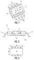
- Fig. 1 is a simplified perspective view of a pair of MOSFETs mounted in a semiconductor package.
- Fig. 2 is a simplified end view of the semiconductor package of Fig. 1.
- Fig. 3 is a simplified top plan view of the package of Fig. 1
- Fig. 4 is a schematic diagram of a typical circuit employing the MOSFETs of Fig. 1.
- Fig. 5 is a cross-sectional view of p-channel MOSFET 10 of Fig. 1.
- Fig. 1 shows a p-channel, enhancement-mode MOSFET 10 packaged adjacent to a smaller, n-channel enhancement-mode MOSFET 12 in a so-called Small Outline Dual In-Line package 14.
- Package 14 may have four leads 16 extending from one side, and four leads 18 extending from another side, although the number of leads may vary.
- MOSFETs 12 and 14 carry substantially equal root mean square (r.m.s.) current levels.
- thermal cooling path 20 from MOSFET 12 to MOSFET 10, shown as a single arrow for convenience, and thermal cooling path 22 from MOSFET 10 to MOSFET 12, shown as a single arrow, should be reduced to a small, and preferably, negligible level compared with remaining thermal cooling paths from the MOSFETs, such as shown at 19 in Fig. 2.
- package 14 can be economically made such that the only metallic thermal cooling paths comprise a lead frame 17, shown in simplified form, connected to leads 16 and 18.
- Fig. 3 illustrates such "main area,” as this term is used in this specification and claims.
- the main area which is the product of dimensions 24 and 26 in the embodiment shown, is preferably no more than about 40.5 square millimeters; more preferably no more than about 35.4 square millimeters; and still more preferably no more than about 20.2 square millimeters.
- the subject thermal issue is particularly significant where the maximum power rating for MOSFETs 10 and 12 collectively is no more than about 1 watt; and, more preferably, no more than about 1 ⁇ 2 watt.
- inter-device thermal transfer is reduced compared with increased thermal transfer through the device package (e.g.. lead frame).
- Fig. 4 shows a ballast circuit 28 for a compact fluorescent lamp 30 employing MOSFETs 10 and 12.
- a d.c. voltage source 32 provides a d.c. voltage between a bus conductor 34 and a reference conductor 36.
- a circuit 38 controls alternate conduction of MOSFETs 10 and 12, usually in response to feedback from a resonant load circuit including lamp 30, a resonant inductor 40 and a resonant capacitor 42.
- Capacitors 44 and 46 maintain the potential of node 48 at about 1 ⁇ 2 the voltage between bus and reference conductors 34 and 36.
- An optional snubber circuit may be formed from capacitor 50 and, optionally, a resistor 52, as further described in U.S. Patent 5,382,882, commonly assigned.
- MOSFET 10 conducts and shorts common node 54 to reference conductor 36. This creates a current 56 which is negative-going with respect to the direction of arrow 56. MOSFET 10 then switches off and MOSFET 12 conducts, connecting node 54 to bus conductor 34. This creates a positive-going current 58 with respect to the direction of arrow 58. Currents 56 and 58 combine at node 54 to form resonant load current 60. The r.m.s. values of currents 56 and 58 are approximately the same in the ballast circuit of Fig. 4.
- Fig. 5 shows a cross section of p-channel enhancement-mode MOSFET 10.
- source 10s and drain 10d electrodes are connected to highly doped p-conductivity regions 62 and 64.
- a gate 10g is separated from inversion channel 66 by an oxide or other electrically insulating layer 68.
- gate 10g creates inversion channel of p-conductivity type.
- the width of the channel, as used herein, is shown by dimension 70, i.e., the separation between regions 62 and 64.
- MOSFET 10 With the mobility of the p-channel of MOSFET 10 being approximately half that of the n-channel of MOSFET 12, and with the same channel widths by way of example, a scaling of the area of the p-channel to approximately twice that of the n-channel would tend to equalize the on-resistances of MOSFETs 10 and 12.
- the range of ratios of channel area of p-channel MOSFET 10 to channel area of n-channel MOSFET 12 should be between about 1.4 and about 2.0; and, more preferably, between about 1.4 and about 1.6.
- lamp 12 may have cathodes, it could alternatively be an electrodeless lamp.
Landscapes
- Electronic Switches (AREA)
- Metal-Oxide And Bipolar Metal-Oxide Semiconductor Integrated Circuits (AREA)
Applications Claiming Priority (2)
| Application Number | Priority Date | Filing Date | Title |
|---|---|---|---|
| US38260 | 1987-04-14 | ||
| US09/038,260 US5929520A (en) | 1998-03-10 | 1998-03-10 | Circuit with small package for mosfets |
Publications (1)
| Publication Number | Publication Date |
|---|---|
| EP0942471A2 true EP0942471A2 (de) | 1999-09-15 |
Family
ID=21898925
Family Applications (1)
| Application Number | Title | Priority Date | Filing Date |
|---|---|---|---|
| EP99301818A Withdrawn EP0942471A2 (de) | 1998-03-10 | 1999-03-10 | Schaltung mit kleiner Packung für MOSFETS |
Country Status (3)
| Country | Link |
|---|---|
| US (1) | US5929520A (de) |
| EP (1) | EP0942471A2 (de) |
| JP (1) | JPH11340340A (de) |
Cited By (1)
| Publication number | Priority date | Publication date | Assignee | Title |
|---|---|---|---|---|
| DE19935100A1 (de) * | 1999-07-27 | 2001-03-15 | Infineon Technologies Ag | Halbbrückenkonfiguration |
Families Citing this family (3)
| Publication number | Priority date | Publication date | Assignee | Title |
|---|---|---|---|---|
| JP4737555B2 (ja) * | 2006-02-10 | 2011-08-03 | 東芝ライテック株式会社 | 電球形蛍光ランプおよび照明装置 |
| US9078380B2 (en) | 2012-10-19 | 2015-07-07 | Nvidia Corporation | MOSFET stack package |
| DE102018118275A1 (de) * | 2018-07-27 | 2020-01-30 | Valeo Siemens Eautomotive Germany Gmbh | Rotoranordnung für eine elektrische Maschine, elektrische Maschine für ein Fahrzeug und Fahrzeug |
Family Cites Families (10)
| Publication number | Priority date | Publication date | Assignee | Title |
|---|---|---|---|---|
| US5489804A (en) * | 1989-08-28 | 1996-02-06 | Lsi Logic Corporation | Flexible preformed planar structures for interposing between a chip and a substrate |
| KR100552353B1 (ko) * | 1992-03-27 | 2006-06-20 | 가부시키가이샤 히타치초엘에스아이시스템즈 | 리이드프레임및그것을사용한반도체집적회로장치와그제조방법 |
| US5598031A (en) * | 1993-06-23 | 1997-01-28 | Vlsi Technology, Inc. | Electrically and thermally enhanced package using a separate silicon substrate |
| JP3233507B2 (ja) * | 1993-08-13 | 2001-11-26 | 株式会社東芝 | 半導体装置 |
| US5585600A (en) * | 1993-09-02 | 1996-12-17 | International Business Machines Corporation | Encapsulated semiconductor chip module and method of forming the same |
| DE59510918D1 (de) * | 1994-08-12 | 2004-08-12 | Infineon Technologies Ag | Halbleiterbauelement mit isolierendem Gehäuse |
| JP2972096B2 (ja) * | 1994-11-25 | 1999-11-08 | シャープ株式会社 | 樹脂封止型半導体装置 |
| JP3485655B2 (ja) * | 1994-12-14 | 2004-01-13 | 株式会社ルネサステクノロジ | 複合型mosfet |
| US5615475A (en) * | 1995-01-30 | 1997-04-01 | Staktek Corporation | Method of manufacturing an integrated package having a pair of die on a common lead frame |
| US5814884C1 (en) * | 1996-10-24 | 2002-01-29 | Int Rectifier Corp | Commonly housed diverse semiconductor die |
-
1998
- 1998-03-10 US US09/038,260 patent/US5929520A/en not_active Expired - Lifetime
-
1999
- 1999-03-09 JP JP11061097A patent/JPH11340340A/ja not_active Withdrawn
- 1999-03-10 EP EP99301818A patent/EP0942471A2/de not_active Withdrawn
Cited By (2)
| Publication number | Priority date | Publication date | Assignee | Title |
|---|---|---|---|---|
| DE19935100A1 (de) * | 1999-07-27 | 2001-03-15 | Infineon Technologies Ag | Halbbrückenkonfiguration |
| DE19935100B4 (de) * | 1999-07-27 | 2004-10-28 | Infineon Technologies Ag | Halbbrückenkonfiguration |
Also Published As
| Publication number | Publication date |
|---|---|
| JPH11340340A (ja) | 1999-12-10 |
| US5929520A (en) | 1999-07-27 |
Similar Documents
| Publication | Publication Date | Title |
|---|---|---|
| US8611108B2 (en) | Electronic circuit control element with tap element | |
| US7436015B2 (en) | Driver for driving a load using a charge pump circuit | |
| JPH10512718A (ja) | シリコン・オン・インシュレータ型集積回路のesd保護を与える方法及び構造体 | |
| US11967545B2 (en) | Semiconductor device | |
| US6924532B2 (en) | Field-effect power transistor | |
| US5719429A (en) | High frequency/high output insulated gate semiconductor device with reduced and balanced gate resistance | |
| US4712124A (en) | Complementary lateral insulated gate rectifiers with matched "on" resistances | |
| KR20000071554A (ko) | 파워 반도체 모듈 | |
| KR20080038207A (ko) | Ldmos 트랜지스터 | |
| US6469352B2 (en) | Two-terminal semiconductor overcurrent limiter | |
| KR950034760A (ko) | 반도체 장치 및 그 제조방법 | |
| US11844198B2 (en) | Power module | |
| US5929520A (en) | Circuit with small package for mosfets | |
| TW556317B (en) | Field effect transistor formed on an insulative substrate and integrated circuit thereof | |
| JP2001358335A (ja) | 半導体装置 | |
| US20040212419A1 (en) | MOSFET circuit having reduced output voltage oscillations during a switch-off operation | |
| JP4363190B2 (ja) | 半導体装置及びその製造方法 | |
| US20030230777A1 (en) | MOSFET and a method for manufacturing the same | |
| US7547946B2 (en) | MOS semiconductor device with low ON resistance | |
| KR100304751B1 (ko) | 상호접촉하여형성된n-형및p-형반도체도체영역을가진반도체집적회로장치 | |
| JP2002353406A (ja) | 半導体装置 | |
| JP6890480B2 (ja) | 半導体装置 | |
| JP2713409B2 (ja) | 相補soi型横方向絶縁ゲート整流器 | |
| JP2021119624A (ja) | 半導体装置及び制御システム | |
| US10368431B2 (en) | Cooling assemblies for electronic devices |
Legal Events
| Date | Code | Title | Description |
|---|---|---|---|
| PUAI | Public reference made under article 153(3) epc to a published international application that has entered the european phase |
Free format text: ORIGINAL CODE: 0009012 |
|
| AK | Designated contracting states |
Kind code of ref document: A2 Designated state(s): AT BE CH CY DE DK ES FI FR GB GR IE IT LI LU MC NL PT SE |
|
| AX | Request for extension of the european patent |
Free format text: AL;LT;LV;MK;RO;SI |
|
| STAA | Information on the status of an ep patent application or granted ep patent |
Free format text: STATUS: THE APPLICATION HAS BEEN WITHDRAWN |
|
| 18W | Application withdrawn |
Effective date: 20030306 |