EP0942555A2 - Procédé et dispositif de communication pour la communication fiable utilisant un réseau bus dupliqué - Google Patents
Procédé et dispositif de communication pour la communication fiable utilisant un réseau bus dupliqué Download PDFInfo
- Publication number
- EP0942555A2 EP0942555A2 EP99103593A EP99103593A EP0942555A2 EP 0942555 A2 EP0942555 A2 EP 0942555A2 EP 99103593 A EP99103593 A EP 99103593A EP 99103593 A EP99103593 A EP 99103593A EP 0942555 A2 EP0942555 A2 EP 0942555A2
- Authority
- EP
- European Patent Office
- Prior art keywords
- bus
- buses
- received
- communication
- arbitration
- Prior art date
- Legal status (The legal status is an assumption and is not a legal conclusion. Google has not performed a legal analysis and makes no representation as to the accuracy of the status listed.)
- Withdrawn
Links
Images








Classifications
-
- H—ELECTRICITY
- H04—ELECTRIC COMMUNICATION TECHNIQUE
- H04L—TRANSMISSION OF DIGITAL INFORMATION, e.g. TELEGRAPHIC COMMUNICATION
- H04L12/00—Data switching networks
- H04L12/28—Data switching networks characterised by path configuration, e.g. LAN [Local Area Networks] or WAN [Wide Area Networks]
- H04L12/40—Bus networks
- H04L12/403—Bus networks with centralised control, e.g. polling
-
- G—PHYSICS
- G06—COMPUTING OR CALCULATING; COUNTING
- G06F—ELECTRIC DIGITAL DATA PROCESSING
- G06F11/00—Error detection; Error correction; Monitoring
- G06F11/07—Responding to the occurrence of a fault, e.g. fault tolerance
- G06F11/16—Error detection or correction of the data by redundancy in hardware
- G06F11/1608—Error detection by comparing the output signals of redundant hardware
- G06F11/1625—Error detection by comparing the output signals of redundant hardware in communications, e.g. transmission, interfaces
-
- H—ELECTRICITY
- H04—ELECTRIC COMMUNICATION TECHNIQUE
- H04L—TRANSMISSION OF DIGITAL INFORMATION, e.g. TELEGRAPHIC COMMUNICATION
- H04L12/00—Data switching networks
- H04L12/28—Data switching networks characterised by path configuration, e.g. LAN [Local Area Networks] or WAN [Wide Area Networks]
- H04L12/40—Bus networks
- H04L12/40169—Flexible bus arrangements
- H04L12/40176—Flexible bus arrangements involving redundancy
- H04L12/40182—Flexible bus arrangements involving redundancy by using a plurality of communication lines
-
- H—ELECTRICITY
- H04—ELECTRIC COMMUNICATION TECHNIQUE
- H04L—TRANSMISSION OF DIGITAL INFORMATION, e.g. TELEGRAPHIC COMMUNICATION
- H04L12/00—Data switching networks
- H04L12/28—Data switching networks characterised by path configuration, e.g. LAN [Local Area Networks] or WAN [Wide Area Networks]
- H04L12/46—Interconnection of networks
- H04L12/4604—LAN interconnection over a backbone network, e.g. Internet, Frame Relay
- H04L12/462—LAN interconnection over a bridge based backbone
- H04L12/4625—Single bridge functionality, e.g. connection of two networks over a single bridge
Definitions
- the present invention relates to a communication system and a communication control method wherein stations are connected to buses to communicate with each other through the buses.
- a computing system In a computing system, the whole circuitry of a system is typically divided into CPU sections, storage unit sections, input/output interface sections, and so on, and a plurality of printed wire boards comprising these sections is installed in the system. These printed wire boards are interconnected by connecting between connectors attached to the boards through a bus. A board provided with connectors and a bus is generally called a backplane. A communication system is built using a backplane to enable printed wire boards in the system to communicate with each other. The prior art and its problems found in a communication system where backplanes were adopted are described separately in the following paragraphs (a) to (e).
- a bus connecting between the stations is often duplicated in order to increase communication reliability.
- the two redundant buses are used alternately as long as both buses are normal. If one of the buses fails, the other normal bus is used to continue communication.
- the processor must be aware of which of the two redundant buses is the active bus or the standby bus.
- Figure 1 is a schematic representation showing an example of the configuration of a conventional communication system.
- a plurality of units 21 to 2n is connected to a bus 1 in a multidrop configuration.
- the units 21 to 2n communicate with each other through the bus.
- Figure 2 is the equivalent circuit of the bus 1.
- the bus 1 has its own inductance L and stray capacitance C.
- a signal transferred through the bus to the unit reflects at points where other units are connected.
- reflected signals occur at the connection points of the units 22 to 2n.
- Figure 3 shows the waveform of a signal at point B.
- Signals reflected by the units 23 to 2n reach point B before the signal received by the unit 22 changes from a high-level state to a low-level state.
- the reflected signals from the units 23 to 2n are superposed with the received signal, as shown in Figure 3, thus increasing the degree of waveform distortion. This may cause the receiving unit 22 to malfunction.
- the magnitude of the superposed reflected signals exceeds the low-level threshold.
- the transmitter circuit of a unit is provided with a driver IC that sends out signals to a bus. If any one bit, among the bits input to the driver IC, is kept static and all other bits are switched at the same time, the ground potential of the driver IC increases. This phenomenon is known as ground bounce; noise may be induced at the static bit due to the effects of the ground bounce. This noise is known as simultaneous switching noise; faulty data may be transferred due to the simultaneous switching noise.
- Figure 4 is a schematic configuration of a standard communication system.
- a transmitter circuit 11 and a receiver circuit 12 are connected to a transmission line 10 that constitutes a bus. Data is transferred from the transmitter circuit 11 to the receiver circuit 12 through the transmission line 10.
- the transmitter circuit 11 and the receiver circuit 12 operate on asynchronous clocks having different phases. Before any signal transfer can be carried out in the communication system, data transmitted using the clock in the transmitter circuit must be somehow synchronized with the clock in the receiver circuit.
- this synchronization is achieved by using a clock faster than the data transfer rate for the receiver circuit to sample the data.
- a clock having a frequency approximately 16 times the data transfer rate is used.
- this synchronization is achieved by writing the data once into a FIFO circuit in the receiver circuit using the transmitted clock signal, and then reading the data from the FIFO circuit using the clock in the receiver circuit.
- the receiver circuit In data transfer based on start-stop synchronization, the receiver circuit must be provided with a clock that operates at speeds higher than the data transmission rate. As a result, the data transmission rate must be lower than the frequency of the clock available for the receiver circuit. For this reason, high-speed signal transfer has been difficult to achieve.
- the data In data transfer based on clock synchronization, the data is once written into a FIFO circuit in the receiver circuit using the transmitted clock signal. For this reason, faulty data may be written into the FIFO circuit if the waveform of a received clock signal is distorted.
- the waveforms of signals that propagate between circuits connected to a transmission line that constitutes a bus are distorted due to the capacitive load of the transmission line or the effects of noise that enters the transmission line. This makes it difficult to achieve high-speed, consistent signal transfer.
- Figure 5 is an example of the schematic configuration of the conventional communication system.
- bus masters 31 to 3n are connected to a data bus 42 and an arbitration bus 43.
- a slave 44 is, for example, a storage unit and is connected to the data bus 42.
- An arbiter 45 is incorporated in each of the bus masters 31 to 3n. The arbiter 45, after having gone through an arbitration procedure using the arbitration bus 43, permits the bus master, which has acquired the right to use the data bus 42, to do so.
- the bus master that has acquired the right to use the data bus 42 gains access to the slave 44.
- Figure 6 is a schematic representation showing the behavior of the conventional communication system shown in Figure 5.
- bus masters 31 and 32 acquire the right to use a data bus 42 in succession in the order of the bus master 31 then 32 and 32 then 31. In this process, an arbitration action using an arbitration bus 43 takes place each time the right of use is acquired.
- the present invention is intended to avoid the problems described in paragraphs (a) to (e) above. Accordingly, it is an object of the present invention to provide a communication system and communication control method whereby communication can be carried out without being aware of the state of a dual-redundant bus; the integrity of data in areas other than the bus can also be examined; and high-speed, highly reliable communication can be achieved.
- Figure 1 is the schematic configuration of an example of a conventional communication system.
- Figure 2 is the equivalent circuit diagram of the bus shown in Figure 1.
- Figure 3 is the schematic waveform of a signal observed at point B.
- Figure 4 is the schematic configuration of a standard communication system.
- Figure 5 is an example of the schematic configuration of a conventional communication system.
- Figure 6 is a schematic representation showing the behavior of the example of the conventional communication system shown in Figure 5.
- Figure 7 is a schematic configuration of one embodiment of the present invention.
- Figure 8 is a schematic representation showing the behavior of the communication procedure control unit shown in Figure 7.
- Figure 9 is another schematic representation showing the behavior of the communication procedure control unit shown in Figure 7.
- Figure 10 is a schematic configuration of another embodiment of the present invention.
- Figure 11 is the schematic waveform of a signal observed at point D.
- Figure 12 is a schematic representation showing an example of the configuration of the bus shown in Figure 10.
- Figure 13 is a schematic representation showing the configuration of yet another embodiment of the present invention.
- Figure 14 is a schematic representation showing an example of the configuration of the transmitter circuit shown in Figure 13.
- Figure 15 is a schematic example of a conversion table for coding.
- Figure 16 is a schematic representation showing an example of the configuration of the receiver circuit shown in Figure 13.
- Figure 17 is a schematic representation showing the configuration of yet another embodiment of the present invention.
- Figure 18 is the timing chart of signals used in the example of the embodiment shown in Figure 17.
- Figure 19 is a schematic configuration of yet another embodiment of the present invention.
- Figure 20 is a schematic configuration of the main part of the embodiment of Figure 19.
- Figure 21 is a schematic representation showing the operation of the embodiment of Figure 19.
- Embodiments 1 to 5 described below are those of communication systems that are free from the problems discussed in paragraphs (a) to (e).
- Embodiments 1 to 5 are described separately in paragraphs (1) to (5).
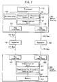
- Figure 7 is a schematic representation showing the configuration of one embodiment of the present invention.
- two redundant buses 151 and 152 are connected to a master station 100.
- Buses 151 and 152 are connected to two redundant buses 171 and 172 through relay equipment 161 and 162, respectively.
- the buses 171 and 172 are connected to a slave station 500.
- the relay equipment 161 and 162, for example, are bridges or repeaters.
- the relay equipment 161 and 162 may be excluded from this embodiment.
- buses 151 and 152 are identical to buses 171 and 172.
- a processor 110 controls the master station as a whole.
- a sequencer 120 is connected to buses 151 and 152 through bus interfaces 131 and 132.
- the sequencer 120 is provided with a communication unit 121, a communication procedure control unit 122 and an annunciator 123, the behavior of which are described later.
- a subordinate unit 510 is a device that operates under the command and control of a master station 100 and is memory in the example shown in Figure 7.
- a sequencer 520 is connected to buses 171 and 172 through bus interfaces 531 and 532.
- the sequencer 520 is provided with a communication unit 521 and a communication procedure control unit 522, the behavior of which are described later.
- the communication unit 121 in the sequencer 120 simultaneously sends out two command frames having the same content to the buses 151 and 152.
- the command frames contain added test bits.
- the transmitted command frames travel through the buses 151 and 152, relay equipment 161 and 162, then buses 171 and 172 to reach the slave station 500.
- the communication unit 521 receives the command frames. Then, the communication procedure control unit 522 processes the received command frames.
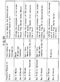
- Figure 8 is a schematic representation showing the behavior of the communication procedure control unit 522.
- the communication procedure control unit 522 performs a test of valid data transfer using check bits on the contents of the two command frames that the slave station receives through the buses 171 and 172, and examines whether or not the contents of the received two command frames match. The communication procedure control unit then executes the processes described below depending on the results of the test and examination.
- the received contents are checked for errors by, for example, means of a cyclic redundancy check (CRC).
- CRC cyclic redundancy check
- command frames which are judged to be normal by means of the check bits, are received.
- the communication unit 521 sends out response frames received from the communication procedure control unit 522 to the buses 171 and 172.
- the communication unit adds check bits to the response frames before it sends them out.
- the communication procedure control unit 122 monitors for responses from the slave station 500.
- Figure 9 is a schematic representation showing the behavior of the communication procedure control unit 122.
- the communication procedure control unit 122 monitors for responses from the slave station 500 and executes the processes described below depending on the results of monitoring.
- the annunciator 123 informs the processor 110 which of the above-mentioned cases [1] to [4] the access to the slave station fell under before it ended.
- the communication procedure control unit 122 sets a status flag that indicates the "state of the bus 171, state of the bus 172 and the conformity of received contents.”
- the processor 110 checks the status flag when it diagnoses the states of buses.
- Figure 10 is a schematic representation showing the configuration of another embodiment of the present invention.
- a plurality of units from 71 to 7n is connected to a bus 60 in a multidrop configuration.
- the line length of the bus 60 satisfies the following conditional formula.
- bus 60 There is a backplane bus as one example of the bus 60.
- Figure 11 shows the schematic waveform observed at a point D.
- the signal received by the unit 72 changes from a high-level state to a low-level state before signals reflected by the other units 73 to 7n reach the point D.
- the signals reflected by the units 73 to 7n never coincide with the transition of the signal received by the unit 72 and are independent of each other. This means the magnitude of superposed reflected signals never crosses the threshold of the low-level state and, therefore, the receiving unit 72 never malfunctions.
- Figure 12 is a schematic representation showing an example of the configuration of the bus 60.
- the bus 60 is structured in a zigzag wiring pattern on a printed wire board 61.
- the line length of the bus 60 is determined so that the transition time of a transmission signal on the bus is shorter than the time required for the transmission signal to make a round trip between any two of the units.
- the transition time of a signal at any receiving unit passes before signals reflected by other units reach the receiving unit.
- the reflected signals are independent of each other, thus preventing the receiving unit from malfunctioning. This suppresses the effects of any reflected signal occurring on the bus.
- the bus is structured in a zigzag wiring pattern on a printed wire board, the overall line length of the bus can be increased by effectively using the narrow space of the board.
- Figure 13 is a schematic representation showing the configuration of yet another embodiment of the present invention.
- a bus 60 consists of a control signal bus 601 and a data bus 602.
- a unit 71 is provided with a transmitter circuit 711 and a unit 72 is provided with a receiver circuit 721.
- Both the transmitter circuit 711 and the receiver circuit 721 may be incorporated in any single unit.
- Figure 14 is a schematic representation showing one example of the configuration of the transmitter circuit 711.
- a logic part 712 outputs the control signal CTL and data D3-0. These are bit signals.
- data D3-0 is 4-bit data.
- An encoder 713 encodes data sent by the logic part 712 into a bit signal having a fixed number of bit 1's.
- data D3-0 which is 4-bit data
- DATA4-0 which is 6-bit data.
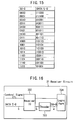
- Figure 15 is an example of a code conversion table.
- An encoder 713 encodes data D3-0 into data DATA4-0 according to this table.
- Data DATA4-0 contains bit 1's whose quantity is fixed at either two or three.
- a driver IC 714 outputs the control signal CTL and data DATA4-0 to a bus 60.
- the number of bit 1's contained in the data DATA4-0 supplied to the driver IC 714 remains fixed at either two or three even if the states of bits in data D3-0 change simultaneously while the states of bits in the control signal CTL are kept static. As a result, the effects of ground bounce are suppressed and the static bits of the control signal CTL are protected against induced noise.
- Figure 16 is a schematic representation showing one example of the configuration of the receiver circuit 721.
- a receiver circuit 722 receives the control signal CTL and data DATA4-0 sent through the bus 60.
- a decoder 723 decodes data DATA4-0 back into data D3-0. As a result, the data transmitted by a transmitter circuit 711 is restored.
- a logic part 724 processes the control signal CTL and data D3-0.
- the number of bits in data before and after coding and the number of bit 1's in data after coding may be other than those mentioned above.
- transmission data is encoded into a bit signal having a fixed number of bit 1's before it is supplied to a driver IC. As a result, it is possible to reduce the effects of ground bounce.
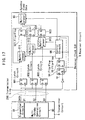
- Figure 17 is a schematic representation of the configuration of yet another embodiment of the present invention.
- a transmitter circuit 8 and a receiver circuit 9 are connected to a transmission line 200.
- a transmitter circuit 81 sends out data DATA to a transmission line 200.
- a multi-strobe generation circuit 82 generates as many as N strobe signals (N is an integer) having different strobe timings onto a transmission line 200.
- the multi-strobe generation circuit generates three strobe signals, i.e., S1, S2 and S3.
- the receiver circuit 9 is provided with as many latch circuits as the number of strobe signals.
- three latch circuits i.e., latch circuits 901, 902 and 903, are provided.
- Data sent by the transmitter circuit 81 is successively retained in the latch circuits 901, 902 and 903, in this order, at the points in time of S1, S2 and S3, respectively. If there are N strobe signals, the receiver circuit is provided with as many latch circuits.
- Outputs of the latch circuits 901, 902 and 903 are supplied to multiplexers 911, 912 and 913.
- Flip-flops 921, 922 and 923 are supplied with selected outputs of the multiplexers 911, 912 and 913, respectively, and at the same time feed their own outputs back to the multiplexers.
- a multiplexer 93 selects one of the outputs of the multiplexers 921, 922 and 923 to output it. This output serves as the synchronized data.
- a flip-flop 94 is a circuit for detecting the starting point of communication and set as triggered by the rising edge of a strobe signal S1.
- a flip-flop 95 synchronizes the strobe signal S1 with the receiver clock CLK.
- the receiver clock CLK has the frequency equivalent to the transmission rate of data DATA.
- a control circuit 96 receives the output of the flip-flop 95 and the receiver clock CLK to control the switching of the multiplexers 911, 912, 913 and 93 and resets the flip-flop 94 at the end of communication.
- the multiplexers 911, 912, 913 and 93, the flip-flops 921, 922, 923, 94 and 95, and the control circuit 96 constitute a sampling circuit that samples data retained in the latch circuits 901, 902 and 903 using the receiver clock CLK having the frequency equivalent to the transmission rate of data DATA, in order to synchronize the data with the receiver clock.
- Figure 18 is a signal timing chart for the embodiment of Figure 17.
- the embodiment is provided with three signals, i.e., S1, S2 and S3.
- the strobe signals are at a high level when no communication is carried out. The moment when a strobe signal changes from a low-level state to a high-level state is the time data is strobed.
- a receiver circuit 8 drives data DATA and the three strobe signals, i.e., S1, S2 and S3, to transmit the data.
- latch circuits 901, 902 and 903 retain data DATA at the timings of strobe signals S1, S2 and S3.
- data A, B and C are retained in the latch circuits 901, 902 and 903.
- the latch circuits 901, 902 and 903 continue to hold the same data until the strobe signals make the next state transition.
- the latch circuit 901 retains data A and continues to hold it until strobe signal S1 changes to a low-level state.
- the sampling circuit samples data retained by the latch circuits 901, 902 and 903 using the receiver clock CLK having the frequency equivalent to the data transmission rate of data DATA to synchronize the data with the receiver clock CLK.
- the receiver clock CLK is not synchronized with strobe signals S1, S2 and S3, the above-mentioned synchronization can still be achieved by sampling the data retained in the latch circuits 901, 902 and 903 using the receiver clock CLK before the data changes.
- data A may be sampled using the receiver clock CLK while the latch circuit 901 is retaining the data.
- a frequency equivalent to the data transmission rate of data DATA is therefore enough for the receiver clock CLK to achieve the synchronization.
- the receiver circuit will not malfunction even if the strobe signals' waveforms become distorted due to the effects of a capacitive load or noise in the transmission line, thus ensuring consistent signal transfer.
- Figure 19 is a schematic representation of the configuration of yet another embodiment of the present invention.
- bus masters 31 to 3n are provided with a pair of a monitor 46 and an arbiter 47.
- the monitor 46 monitors signals on an arbitration bus 43.
- the arbiter 47 once a request to use the data bus is issued from the bus master to which the arbiter belongs, executes the following processes depending on the results of monitoring by the monitor 46.
- Figure 20 is a schematic representation of the main part of the embodiment of Figure 19.
- a bus master 48 sends signal BR requesting to acquire the right to use the bus to an arbiter 47.
- the bus master receives signal BG for informing acquisition of the right, it transmits data using a data bus 42.
- the signal line of the arbitration bus 43 carries signals REQ3 to REQ0, which represent a request for the right to use the bus made by a bus master 30, as well as REQOUT signal.
- Signals REQ3 to REQ0 are input signals to the bus master 30 and REQOUT signal is an output signal from the bus master.
- Output REQOUT signal is supplied to the signal line of one of signals REQ3 to REQ0.
- Signals REQ3 to REQ0 are prioritized in the order of REQ0, REQ1, REQ2 and REQ3.
- the number of signal lines need not be limited to the quantity mentioned herein.
- arbitration is carried out according to the procedure described below.
- bus master 30 If the bus master 30 is in a neutral state, there is no request from that bus master to use the bus. In this state, the data bus 42 or the output REQOUT signal is not driven from the bus master 30.
- the bus master 30 makes its own REQOUT signal active without delay, after confirming that signals REQ3 to REQ0 on the arbitration bus 43 are inactive.
- the bus master 30 After sending out the REQOUT signal, the bus master 30 compares each of signals REQ3 to REQ0 on the arbitration bus 43 with its own REQOUT signal to find the order of priority, and then executes the following processes.
- the bus master 48 transfers data using the data bus 42. While the data bus 42 is in use, the bus master 30 continues outputting the REQOUT signal.
- the bus master 30 releases the data bus 42 and withdraws the REQOUT signal.
- the monitor 46 monitors signals REQ3 to REQ0 on the arbitration bus 43. If another bus master issues any of signals REQ3 to REQ0, the monitor 46 brings its own bus master 30 into a neutral state. In that case, the monitor 46 forces its own bus master 30 to enter the neutral state even if one of the signals among REQ3 to REQ0 has a lower priority than that of the bus master 30's own REQOUT signal.
- the bus master 30 uses the bus again.
- the bus master 30 When reusing the data bus 42, the bus master 30 activates the REQOUT signal to immediately acquire the right to use the data bus. More specifically, the bus master immediately acquires the right without going through the arbitration procedure using the arbitration bus 43.
- Figure 21 is a schematic representation of the behavior of the embodiment of Figure 19.
- a master station 32 uses a data bus 42 in two consecutive rounds. If there is no request issued by other bus masters to use the data bus when the master station 32 uses the data bus the second time, the master station immediately acquires the right to use the data bus without going through the arbitration procedure.
- any given bus master is permitted to acquire the right to use the data bus without going through the arbitration procedure using the arbitration bus, if in a case where the bus master uses the data bus again, no arbitration is carried out after the bus master has finished using the data bus. Subsequently, it is possible to save any wasteful arbitration time and improve system performance.
Landscapes
- Engineering & Computer Science (AREA)
- Theoretical Computer Science (AREA)
- Computer Networks & Wireless Communication (AREA)
- Signal Processing (AREA)
- Quality & Reliability (AREA)
- Physics & Mathematics (AREA)
- General Engineering & Computer Science (AREA)
- General Physics & Mathematics (AREA)
- Small-Scale Networks (AREA)
- Communication Control (AREA)
- Bus Control (AREA)
Priority Applications (1)
| Application Number | Priority Date | Filing Date | Title |
|---|---|---|---|
| EP04021830A EP1484870B1 (fr) | 1998-02-24 | 1999-02-24 | Système de communication et procédé de commande associé |
Applications Claiming Priority (8)
| Application Number | Priority Date | Filing Date | Title |
|---|---|---|---|
| JP4234798 | 1998-02-24 | ||
| JP04234798A JP3552149B2 (ja) | 1998-02-24 | 1998-02-24 | 通信制御装置及び通信制御方法 |
| JP4313298 | 1998-02-25 | ||
| JP4313298A JPH11242652A (ja) | 1998-02-25 | 1998-02-25 | バス調停装置及びバス調停方法 |
| JP04730998A JP3463212B2 (ja) | 1998-02-27 | 1998-02-27 | データ伝達装置 |
| JP4730998 | 1998-02-27 | ||
| JP4731098 | 1998-02-27 | ||
| JP04731098A JP3493650B2 (ja) | 1998-02-27 | 1998-02-27 | 通信装置 |
Related Child Applications (1)
| Application Number | Title | Priority Date | Filing Date |
|---|---|---|---|
| EP04021830A Division EP1484870B1 (fr) | 1998-02-24 | 1999-02-24 | Système de communication et procédé de commande associé |
Publications (2)
| Publication Number | Publication Date |
|---|---|
| EP0942555A2 true EP0942555A2 (fr) | 1999-09-15 |
| EP0942555A3 EP0942555A3 (fr) | 2003-09-10 |
Family
ID=27461186
Family Applications (1)
| Application Number | Title | Priority Date | Filing Date |
|---|---|---|---|
| EP99103593A Withdrawn EP0942555A3 (fr) | 1998-02-24 | 1999-02-24 | Procédé et dispositif de communication pour la communication fiable utilisant un réseau bus dupliqué |
Country Status (3)
| Country | Link |
|---|---|
| US (3) | US6556583B1 (fr) |
| EP (1) | EP0942555A3 (fr) |
| SG (1) | SG142166A1 (fr) |
Cited By (4)
| Publication number | Priority date | Publication date | Assignee | Title |
|---|---|---|---|---|
| DE19921589C2 (de) * | 1999-05-05 | 2002-10-24 | Siemens Ag | Verfahren zum Betrieb eines Datenübertragungssystems |
| EP1462942A1 (fr) * | 2003-03-26 | 2004-09-29 | ROLLS-ROYCE plc | Système de contrôle avec des connexions redondantes permettant de détecter des adresses configurées incorrectement |
| US7913005B2 (en) * | 2000-08-11 | 2011-03-22 | Round Rock Research, Llc | Capacitive multidrop bus compensation |
| EP2226220A4 (fr) * | 2007-12-26 | 2011-05-25 | Honda Motor Co Ltd | Système de communication redondant |
Families Citing this family (17)
| Publication number | Priority date | Publication date | Assignee | Title |
|---|---|---|---|---|
| US7643481B2 (en) * | 1999-03-17 | 2010-01-05 | Broadcom Corporation | Network switch having a programmable counter |
| US7184441B1 (en) * | 1999-03-17 | 2007-02-27 | Broadcom Corporation | Network switch stacking configuration |
| US6859454B1 (en) * | 1999-06-30 | 2005-02-22 | Broadcom Corporation | Network switch with high-speed serializing/deserializing hazard-free double data rate switching |
| ATE252298T1 (de) * | 1999-11-16 | 2003-11-15 | Broadcom Corp | Verfahren und netzwerkvermittlungsstelle mit datenserialisierung durch gefahrlose mehrstufige störungsfreie multiplexierung |
| US6661860B1 (en) * | 2000-01-04 | 2003-12-09 | Massachusetts Institute Of Technology | Multiple arbiter jitter estimation system and related techniques |
| DE10119151A1 (de) * | 2001-04-19 | 2002-12-05 | Phoenix Contact Gmbh & Co | Diagnose-Einrichtung für einen Feldbus mit steuerungsunabhängiger Informationsübermittlung |
| JP3804824B2 (ja) * | 2001-09-19 | 2006-08-02 | ヤマハ株式会社 | ディジタルミキサ |
| US7180966B2 (en) * | 2001-10-26 | 2007-02-20 | International Business Machines Corporation | Transition detection, validation and memorization circuit |
| US7406646B2 (en) * | 2002-10-01 | 2008-07-29 | Advantest Corporation | Multi-strobe apparatus, testing apparatus, and adjusting method |
| JP4002811B2 (ja) * | 2002-10-04 | 2007-11-07 | 株式会社アドバンテスト | マルチストローブ生成装置、試験装置、及び調整方法 |
| US7022919B2 (en) * | 2003-06-30 | 2006-04-04 | Intel Corporation | Printed circuit board trace routing method |
| JP2005352936A (ja) * | 2004-06-14 | 2005-12-22 | Matsushita Electric Ind Co Ltd | スレーブデバイス |
| KR100606244B1 (ko) * | 2005-02-11 | 2006-07-28 | 삼성전자주식회사 | 데이터 스트로브 신호에 동기 되어 전송되는 데이터의 캡쳐 방법 및 이를 위한 데이터 캡쳐 회로 |
| IT1391785B1 (it) * | 2008-11-21 | 2012-01-27 | St Microelectronics Srl | Sistema elettronico per il rilevamento di un guasto |
| CN107957692B (zh) * | 2016-10-14 | 2020-06-09 | 中国石油天然气集团公司 | 控制器冗余方法、装置及系统 |
| CN109617834B (zh) * | 2019-02-01 | 2021-08-24 | 国网江苏省电力有限公司 | 一种精准切负荷系统及其通信方法、接入装置 |
| US11204884B1 (en) * | 2019-06-13 | 2021-12-21 | Rockwell Collins, Inc. | Adapter for synthetic or redundant remote terminals on single 1553 bus |
Family Cites Families (16)
| Publication number | Priority date | Publication date | Assignee | Title |
|---|---|---|---|---|
| CA1129036A (fr) * | 1978-05-30 | 1982-08-03 | Colin R. Betts | Transmission de donnees numeriques |
| US4245344A (en) * | 1979-04-02 | 1981-01-13 | Rockwell International Corporation | Processing system with dual buses |
| US4304001A (en) * | 1980-01-24 | 1981-12-01 | Forney Engineering Company | Industrial control system with interconnected remotely located computer control units |
| US4493021A (en) * | 1981-04-03 | 1985-01-08 | The United States Of America As Represented By The Administrator Of The National Aeronautics And Space Administration | Multicomputer communication system |
| US4569050A (en) * | 1983-01-14 | 1986-02-04 | Honeywell Inc. | Data communication system with fixed weight error correction and detection code |
| US4695952A (en) * | 1984-07-30 | 1987-09-22 | United Technologies Corporation | Dual redundant bus interface circuit architecture |
| US4939728A (en) * | 1987-11-10 | 1990-07-03 | Echelon Systems Corp. | Network and intelligent cell for providing sensing bidirectional communications and control |
| US4811364A (en) * | 1988-04-01 | 1989-03-07 | Digital Equipment Corporation | Method and apparatus for stabilized data transmission |
| US4924463A (en) * | 1989-03-02 | 1990-05-08 | Digital Equipment Corporation | Data coding method for use in digital communication systems |
| US5625644A (en) * | 1991-12-20 | 1997-04-29 | Myers; David J. | DC balanced 4B/8B binary block code for digital data communications |
| US5359630A (en) * | 1992-08-13 | 1994-10-25 | Digital Equipment Corporation | Method and apparatus for realignment of synchronous data |
| AU8018894A (en) * | 1993-11-09 | 1995-05-29 | Advanced Techcom, Inc. | Reducing errors in digital communication |
| DE4339122A1 (de) * | 1993-11-16 | 1995-05-18 | Siemens Ag | Verfahren und Einrichtung zur Steuerung des Zugriffs auf mehrere redundant ausgeführte Übertragungskanäle |
| JPH0846648A (ja) * | 1994-07-29 | 1996-02-16 | Okuma Mach Works Ltd | 通信装置 |
| US5570388A (en) * | 1994-09-27 | 1996-10-29 | Digital Ocean, Inc. | Method and apparatus using simple codes for the wireless transmission of non-data symbols |
| US5606317A (en) * | 1994-12-09 | 1997-02-25 | Lucent Technologies Inc. | Bandwidth efficiency MBNB coding and decoding method and apparatus |
-
1999
- 1999-02-22 US US09/255,427 patent/US6556583B1/en not_active Expired - Fee Related
- 1999-02-24 EP EP99103593A patent/EP0942555A3/fr not_active Withdrawn
- 1999-02-24 SG SG200600276-0A patent/SG142166A1/en unknown
-
2002
- 2002-09-23 US US10/252,493 patent/US6973103B2/en not_active Expired - Fee Related
- 2002-11-04 US US10/287,766 patent/US6952404B2/en not_active Expired - Fee Related
Cited By (6)
| Publication number | Priority date | Publication date | Assignee | Title |
|---|---|---|---|---|
| DE19921589C2 (de) * | 1999-05-05 | 2002-10-24 | Siemens Ag | Verfahren zum Betrieb eines Datenübertragungssystems |
| US6891801B1 (en) | 1999-05-05 | 2005-05-10 | Siemens Aktiengesellschaft | Method of operating a data transmission system |
| US7913005B2 (en) * | 2000-08-11 | 2011-03-22 | Round Rock Research, Llc | Capacitive multidrop bus compensation |
| EP1462942A1 (fr) * | 2003-03-26 | 2004-09-29 | ROLLS-ROYCE plc | Système de contrôle avec des connexions redondantes permettant de détecter des adresses configurées incorrectement |
| US7706931B2 (en) | 2003-03-26 | 2010-04-27 | Rolls-Royce Plc | Control system |
| EP2226220A4 (fr) * | 2007-12-26 | 2011-05-25 | Honda Motor Co Ltd | Système de communication redondant |
Also Published As
| Publication number | Publication date |
|---|---|
| US20030035369A1 (en) | 2003-02-20 |
| EP0942555A3 (fr) | 2003-09-10 |
| US20030081541A1 (en) | 2003-05-01 |
| US6973103B2 (en) | 2005-12-06 |
| SG142166A1 (en) | 2008-05-28 |
| US6952404B2 (en) | 2005-10-04 |
| US6556583B1 (en) | 2003-04-29 |
Similar Documents
| Publication | Publication Date | Title |
|---|---|---|
| EP0942555A2 (fr) | Procédé et dispositif de communication pour la communication fiable utilisant un réseau bus dupliqué | |
| US6490641B2 (en) | Addressable shadow port circuit | |
| EP1484870B1 (fr) | Système de communication et procédé de commande associé | |
| US5349654A (en) | Fault tolerant data exchange unit | |
| US5617420A (en) | Hierarchical connection method, apparatus, and protocol | |
| US5640521A (en) | Addressable shadow port and protocol with remote I/O, contol and interrupt ports | |
| KR100322721B1 (ko) | 버스 내의 스큐를 경감시키는 시스템 및 방법 | |
| EP0578386A2 (fr) | Méthode, appareil et protocole de connexion hiérarchique | |
| WO1997000481A1 (fr) | Dispositif et procede servant a effectuer l'extension a distance d'emplacements pour pci | |
| EP1010296A1 (fr) | Systeme de communications redondant et bon marche | |
| JP2000013414A (ja) | 装置内監視制御システム | |
| US6636100B1 (en) | Can controller and one-chip computer having a built-in can controller | |
| US4639859A (en) | Priority arbitration logic for a multi-master bus system | |
| US6810454B2 (en) | Information processing apparatus having a bus using the protocol of the acknowledge type in the source clock synchronous system | |
| US7653764B2 (en) | Fault-tolerant computer and method of controlling data transmission | |
| US11374846B1 (en) | Lin master testing device | |
| WO1995020193A1 (fr) | Protocole de bus ameliore utilisant des horloges separees pour l'arbitrage et le transfert de donnees | |
| CN114003543B (zh) | 一种高速串行总线时钟补偿方法及系统 | |
| EP0063140A1 (fr) | Structure de bus de communication de donnees | |
| US6343102B1 (en) | In-station control system and method | |
| KR0146743B1 (ko) | 전전자교환기에서 직렬버스 이중화 통신 로직의 중재장치 | |
| CN121887570A (zh) | 一种具有应答占网机制的高可靠rs485总线通信系统 | |
| KR100233100B1 (ko) | 시분할 액서스방식을 채용한 다중 프로세서의 데이타 통신장치 | |
| Bonikowski et al. | Xerox's distributed real time control system | |
| JP2001022710A (ja) | 複数のバス制御装置を有するシステム |
Legal Events
| Date | Code | Title | Description |
|---|---|---|---|
| PUAI | Public reference made under article 153(3) epc to a published international application that has entered the european phase |
Free format text: ORIGINAL CODE: 0009012 |
|
| AK | Designated contracting states |
Kind code of ref document: A2 Designated state(s): AT BE CH CY DE DK ES FI FR GB GR IE IT LI LU MC NL PT SE |
|
| AX | Request for extension of the european patent |
Free format text: AL;LT;LV;MK;RO;SI |
|
| PUAL | Search report despatched |
Free format text: ORIGINAL CODE: 0009013 |
|
| AK | Designated contracting states |
Kind code of ref document: A3 Designated state(s): AT BE CH CY DE DK ES FI FR GB GR IE IT LI LU MC NL PT SE |
|
| AX | Request for extension of the european patent |
Extension state: AL LT LV MK RO SI |
|
| 17P | Request for examination filed |
Effective date: 20031021 |
|
| 17Q | First examination report despatched |
Effective date: 20040311 |
|
| AKX | Designation fees paid |
Designated state(s): DE GB NL |
|
| STAA | Information on the status of an ep patent application or granted ep patent |
Free format text: STATUS: THE APPLICATION IS DEEMED TO BE WITHDRAWN |
|
| 18D | Application deemed to be withdrawn |
Effective date: 20041123 |