EP1484870B1 - Système de communication et procédé de commande associé - Google Patents
Système de communication et procédé de commande associé Download PDFInfo
- Publication number
- EP1484870B1 EP1484870B1 EP04021830A EP04021830A EP1484870B1 EP 1484870 B1 EP1484870 B1 EP 1484870B1 EP 04021830 A EP04021830 A EP 04021830A EP 04021830 A EP04021830 A EP 04021830A EP 1484870 B1 EP1484870 B1 EP 1484870B1
- Authority
- EP
- European Patent Office
- Prior art keywords
- data
- bus
- receiver
- circuit
- bit
- Prior art date
- Legal status (The legal status is an assumption and is not a legal conclusion. Google has not performed a legal analysis and makes no representation as to the accuracy of the status listed.)
- Expired - Lifetime
Links
Images



Classifications
-
- H—ELECTRICITY
- H04—ELECTRIC COMMUNICATION TECHNIQUE
- H04L—TRANSMISSION OF DIGITAL INFORMATION, e.g. TELEGRAPHIC COMMUNICATION
- H04L12/00—Data switching networks
- H04L12/02—Details
- H04L12/12—Arrangements for remote connection or disconnection of substations or of equipment thereof
-
- H—ELECTRICITY
- H04—ELECTRIC COMMUNICATION TECHNIQUE
- H04L—TRANSMISSION OF DIGITAL INFORMATION, e.g. TELEGRAPHIC COMMUNICATION
- H04L12/00—Data switching networks
- H04L12/28—Data switching networks characterised by path configuration, e.g. LAN [Local Area Networks] or WAN [Wide Area Networks]
- H04L12/40—Bus networks
- H04L12/40169—Flexible bus arrangements
- H04L12/40176—Flexible bus arrangements involving redundancy
- H04L12/40182—Flexible bus arrangements involving redundancy by using a plurality of communication lines
-
- H—ELECTRICITY
- H04—ELECTRIC COMMUNICATION TECHNIQUE
- H04L—TRANSMISSION OF DIGITAL INFORMATION, e.g. TELEGRAPHIC COMMUNICATION
- H04L12/00—Data switching networks
- H04L12/28—Data switching networks characterised by path configuration, e.g. LAN [Local Area Networks] or WAN [Wide Area Networks]
- H04L12/40—Bus networks
- H04L12/403—Bus networks with centralised control, e.g. polling
Definitions
- the two redundant buses are used alternately as long as both buses are normal. If one of the buses fails, the other normal bus is used to continue communication. Meanwhile, concurrent communication is carried out in order to check periodically whether or not the failed bus has recovered.
- Figure 1 is a schematic representation showing an example of the configuration of a conventional communication system.
- the bus 1 has its own inductance L and stray capacitance C.
- this synchronization is achieved by writing the data once into a FIFO circuit in the receiver circuit using the transmitted clock signal, and then reading the data from the FIFO circuit using the clock in the receiver circuit.
- the data In data transfer based on clock synchronization, the data is once written into a FIFO circuit in the receiver circuit using the transmitted clock signal. For this reason, faulty data may be written into the FIFO circuit if the waveform of a received clock signal is distorted.
- the waveforms of signals that propagate between circuits connected to a transmission line that constitutes a bus are distorted due to the capacitive load of the transmission line or the effects of noise that enters the transmission line. This makes it difficult to achieve high-speed, consistent signal transfer.
- Figure 5 is an example of the schematic configuration of the conventional communication system.
- a communication system according to the pre-characterizing part of claim 1 is known from US-A-5 359 630 .
- Figure 7 is a schematic representation showing the configuration of one embodiment of the present invention.
- the relay equipment 161 and 162 may be excluded from this embodiment.
- buses 151 and 152 are identical to buses 171 and 172.
- the communication procedure control unit 122 monitors for responses from the slave station 500.
- Figure 9 is a schematic representation showing the behavior of the communication procedure control unit 122.
- the bus 60 is structured in a zigzag wiring pattern on a printed wire board 61.
- the bus is structured in a zigzag wiring pattern on a printed wire board, the overall line length of the bus can be increased by effectively using the narrow space of the board.
- An encoder 713 encodes data sent by the logic part 712 into a bit signal having a fixed number of bit 1's.
- data D3-0 which is 4-bit data
- DATA4-0 which is 6-bit data.
- An encoder 713 encodes data D3-0 into data DATA4-0 according to this table.
- Data DATA4-0 contains bit 1's whose quantity is fixed at either two or three.
- a logic part 724 processes the control signal CTL and data D3-0.
- the number of bits in data before and after coding and the number of bit 1's in data after coding may be other than those mentioned above.
- transmission data is encoded into a bit signal having a fixed number of bit 1's before it is supplied to a driver IC. As a result, it is possible to reduce the effects of ground bounce.
- the multiplexers 911, 912, 913 and 93, the flip-flops 921, 922, 923, 94 and 95, and the control circuit 96 constitute a sampling circuit that samples data retained in the latch circuits 901, 902 and 903 using the receiver clock CLK having the frequency equivalent to the transmission rate of data DATA, in order to synchronize the data with the receiver clock.
- data A, B and C are retained in the latch circuits 901, 902 and 903.
- the latch circuits 901, 902 and 903 continue to hold the same data until the strobe signals make the next state transition.
- the latch circuit 901 retains data A and continues to hold it until strobe signal S1 changes to a low-level state.
- the sampling circuit samples data retained by the latch circuits 901, 902 and 903 using the receiver clock CLK having the frequency equivalent to the data transmission rate of data DATA to synchronize the data with the receiver clock CLK.
- the receiver clock CLK is not synchronized with strobe signals S1, S2 and S3, the above-mentioned synchronization can still be achieved by sampling the data retained in the latch circuits 901, 902 and 903 using the receiver clock CLK before the data changes.
- data A may be sampled using the receiver clock CLK while the latch circuit 901 is retaining the data.
- a frequency equivalent to the data transmission rate of data DATA is therefore enough for the receiver clock CLK to achieve the synchronization.
- the arbiter 47 once a request to use the data bus is issued from the bus master to which the arbiter belongs, executes the following processes depending on the results of monitoring by the monitor 46.
- arbitration is carried out according to the procedure described below.
- the bus master 30 After sending out the REQOUT signal, the bus master 30 compares each of signals REQ3 to REQ0 on the arbitration bus 43 with its own REQOUT signal to find the order of priority, and then executes the following processes.
- the bus master 48 transfers data using the data bus 42. While the data bus 42 is in use, the bus master 30 continues outputting the REQOUT signal. When the data bus is no longer in use, the bus master 30 releases the data bus 42 and withdraws the REQOUT signal.
- the monitor 46 monitors signals REQ3 to REQ0 on the arbitration bus 43. If another bus master issues any of signals REQ3 to REQ0, the monitor 46 brings its own bus master 30 into a neutral state. In that case, the monitor 46 forces its own bus master 30 to enter the neutral state even if one of the signals among REQ3 to REQ0 has a lower priority than that of the bus master 30's own REQOUT signal.
- the bus master 30 When reusing the data bus 42, the bus master 30 activates the REQOUT signal to immediately acquire the right to use the data bus. More specifically, the bus master immediately acquires the right without going through the arbitration procedure using the arbitration bus 43. This saves any wasteful arbitration time.
- the bus master 30 finishes using the data bus 42 it releases the data bus and then withdraws the REQOUT signal to monitor for requests to use the data bus. That is, the bus master moves to the condition described in item (E).
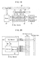
- Figure 21 is a schematic representation of the behavior of the embodiment of Figure 19 .
- a master station 32 uses a data bus 42 in two consecutive rounds. If there is no request issued by other bus masters to use the data bus when the master station 32 uses the data bus the second time, the master station immediately acquires the right to use the data bus without going through the arbitration procedure. This saves any wasteful arbitration time.
- any given bus master is permitted to acquire the right to use the data bus without going through the arbitration procedure using the arbitration bus, if in a case where the bus master uses the data bus again, no arbitration is carried out after the bus master has finished using the data bus. Subsequently, it is possible to save any wasteful arbitration time and improve system performance.
- the advantages of this embodiment are particularly remarkable in cases where a particular bus master uses the bus very frequently.
Landscapes
- Engineering & Computer Science (AREA)
- Computer Networks & Wireless Communication (AREA)
- Signal Processing (AREA)
- Small-Scale Networks (AREA)
- Bus Control (AREA)
Claims (4)
- Système de communication, dans lequel un circuit d'émetteur (8) et un circuit de récepteur (9) sont connectés à une ligne de transmission (200) formant un bus et des données sont transférées entre le circuit d'émetteur (8) et le circuit de récepteur (9),
le circuit d'émetteur comprenant :des moyens formant émetteur (81) pour émettre des données ;le circuit de récepteur comprenant :caractérisé en ce queune pluralité de circuits de bascule (901, 902, 903) pour retenir successivement les données envoyées par le circuit d'émetteur (8) ; etdes moyens d'échantillonnage (93, 94, 95, 96, 911, 912, 91N, 921, 922, 92N) pour échantillonner les données retenues par cette pluralité de circuits de bascule (901, 902, 903) en utilisant une horloge de récepteur (CLK) ayant une fréquence équivalente au débit d'émission de données, de manière à permettre une synchronisation de la réception de données avec l'horloge de récepteur ;
le circuit d'émetteur (8) comprend en outre des moyens de génération d'impulsions multiples (82) pour générer N signaux impulsionnels, dans lequel N est un entier, chacun d'eux ayant une synchronisation différente ; et
le circuit de récepteur (9) comprend des circuits de bascule (901, 902, 903) en un nombre égal au nombre des N signaux impulsionnels pour retenir successivement les données envoyées par le circuit d'émetteur (8) à chaque instant desdits N signaux impulsionnels. - Système de communication selon la revendication 1, caractérisé en ce que
ledit bus comprend un bus de signal de commande (S1, S2, S3) et un bus de données (DATA) disposés parallèlement l'un à l'autre pour transférer en parallèle une pluralité de signaux de commande et de données ;
ledit circuit d'émetteur (8) est connecté audit bus de signal de commande et audit bus de données pour délivrer lesdits signaux de commande et lesdites données audit bus ; et
ledit circuit de récepteur (9) est connecté audit bus de signal de commande et audit bus de données pour recevoir lesdits signaux de commande et lesdites données transmis par l'intermédiaire dudit bus ;
dans lequel ledit circuit d'émetteur (8) comprend :une partie logique (712) ;un codeur (713) ; etun circuit intégré de dispositif de commande (714), ledit codeur (713) étant disposé entre ladite partie logique (712) et ledit circuit intégré de dispositif de commande (714) et codant les données ayant un nombre non fixe de 1 binaires et délivrées par ladite partie logique en un signal binaire ayant un nombre fixe de 1 binaires ; ladite partie logique (712) étant également connectée audit circuit intégré de dispositif de commande (714) pour délivrer des signaux de commande audit circuit intégré de dispositif de commande (714) ; etdans lequel ledit circuit intégré de dispositif de commande (714) délivre lesdits signaux de commande audit bus de signal de commande et les données codées audit bus de données, lesdites données codées contenant un nombre fixe de 1 binaires tandis que l'état des bits dans ledit signal de commande est maintenu statique de sorte qu'un rebond de masse soit supprimé et que les bits statiques dudit signal de commande soient protégés du bruit induit. - Système selon la revendication 2, caractérisé en ce que lesdits moyens formant circuit d'émetteur (8) comprennent en outre :une table de conversion de code ; etdans lequel ledit codeur (713) utilise ladite table de conversion de code pour coder les données ayant un nombre non fixe de 1 binaires en des données codées ayant un nombre fixe prédéterminé de 1 binaires.
- Système selon la revendication 2, caractérisé en ce qu'il comprend une pluralité de circuits de récepteur (9), dans lequel ledit au moins un circuit de récepteur (9) comprend :un circuit intégré de récepteur (722) connecté audit bus de signal de commande et audit bus de données ;un décodeur (723) connecté audit circuit intégré de récepteur (722) pour décoder les données ayant un nombre fixe de 1 binaires de retour en un nombre non fixe d'origine de 1 binaires ; etune partie logique (724) connectée audit circuit intégré de récepteur (722) et audit décodeur (723) pour recevoir lesdits signaux de commande et lesdites données après décodage.
Applications Claiming Priority (7)
| Application Number | Priority Date | Filing Date | Title |
|---|---|---|---|
| JP04234798A JP3552149B2 (ja) | 1998-02-24 | 1998-02-24 | 通信制御装置及び通信制御方法 |
| JP4234798 | 1998-02-24 | ||
| JP4313298A JPH11242652A (ja) | 1998-02-25 | 1998-02-25 | バス調停装置及びバス調停方法 |
| JP4313298 | 1998-02-25 | ||
| JP04730998A JP3463212B2 (ja) | 1998-02-27 | 1998-02-27 | データ伝達装置 |
| JP4730998 | 1998-02-27 | ||
| EP99103593A EP0942555A3 (fr) | 1998-02-24 | 1999-02-24 | Procédé et dispositif de communication pour la communication fiable utilisant un réseau bus dupliqué |
Related Parent Applications (2)
| Application Number | Title | Priority Date | Filing Date |
|---|---|---|---|
| EP99103593A Division EP0942555A3 (fr) | 1998-02-24 | 1999-02-24 | Procédé et dispositif de communication pour la communication fiable utilisant un réseau bus dupliqué |
| EP99103593.2 Division | 1999-02-24 |
Publications (3)
| Publication Number | Publication Date |
|---|---|
| EP1484870A2 EP1484870A2 (fr) | 2004-12-08 |
| EP1484870A3 EP1484870A3 (fr) | 2008-08-27 |
| EP1484870B1 true EP1484870B1 (fr) | 2011-03-30 |
Family
ID=27291171
Family Applications (1)
| Application Number | Title | Priority Date | Filing Date |
|---|---|---|---|
| EP04021830A Expired - Lifetime EP1484870B1 (fr) | 1998-02-24 | 1999-02-24 | Système de communication et procédé de commande associé |
Country Status (4)
| Country | Link |
|---|---|
| EP (1) | EP1484870B1 (fr) |
| KR (1) | KR100361856B1 (fr) |
| CN (1) | CN1144132C (fr) |
| DE (1) | DE69943322D1 (fr) |
Cited By (1)
| Publication number | Priority date | Publication date | Assignee | Title |
|---|---|---|---|---|
| CN111510352A (zh) * | 2020-04-15 | 2020-08-07 | 南京芯欣德科技有限公司 | 一种应用于大规模停车位管理的带轮询查障和心跳状态汇报的总线系统 |
Families Citing this family (12)
| Publication number | Priority date | Publication date | Assignee | Title |
|---|---|---|---|---|
| US7617343B2 (en) * | 2005-03-02 | 2009-11-10 | Qualcomm Incorporated | Scalable bus structure |
| FR2887741B1 (fr) * | 2005-06-24 | 2007-07-27 | Schneider Electric Ind Sas | Bus de communication et tableau electrique comportant un tel bus |
| CN100375448C (zh) * | 2005-11-04 | 2008-03-12 | 北京和利时系统工程股份有限公司 | 一种避免冗余主站对串行总线链路访问冲突的方法 |
| CN100573382C (zh) * | 2006-01-26 | 2009-12-23 | 中控科技集团有限公司 | 基于i2c的通信系统及通信方法 |
| CN100461145C (zh) * | 2006-05-08 | 2009-02-11 | 中兴通讯股份有限公司 | 一种异步ahb互连矩阵接口装置 |
| CN101943898B (zh) * | 2008-09-11 | 2012-03-28 | 深圳市通业科技发展有限公司 | 车列实时控制系统 |
| CN102098196B (zh) * | 2010-12-10 | 2016-04-13 | 曙光信息产业(北京)有限公司 | 刀片服务器的数据传输方法 |
| CN102654550A (zh) * | 2011-07-18 | 2012-09-05 | 张滕飞 | 利用介质损耗变化测试电缆故障的方法 |
| US20140297000A1 (en) * | 2011-11-30 | 2014-10-02 | Mitsubishi Electric Corporation | Control system, control device, connecting line, and drive device |
| CN105045181A (zh) * | 2015-07-24 | 2015-11-11 | 重庆川仪自动化股份有限公司 | Pas100控制系统的总体冗余构架 |
| CN106776436B (zh) * | 2017-01-12 | 2019-11-26 | 烽火通信科技股份有限公司 | 一种适用于多点互联的高速串行总线的通信方法 |
| CN108965119B (zh) * | 2018-09-10 | 2021-05-25 | 杭州和利时自动化有限公司 | 一种智能网关 |
Family Cites Families (5)
| Publication number | Priority date | Publication date | Assignee | Title |
|---|---|---|---|---|
| US4569050A (en) * | 1983-01-14 | 1986-02-04 | Honeywell Inc. | Data communication system with fixed weight error correction and detection code |
| JPH0787462B2 (ja) * | 1988-02-01 | 1995-09-20 | 株式会社東芝 | バス型二重化伝送装置 |
| US5359630A (en) * | 1992-08-13 | 1994-10-25 | Digital Equipment Corporation | Method and apparatus for realignment of synchronous data |
| JPH0846648A (ja) * | 1994-07-29 | 1996-02-16 | Okuma Mach Works Ltd | 通信装置 |
| US5606317A (en) * | 1994-12-09 | 1997-02-25 | Lucent Technologies Inc. | Bandwidth efficiency MBNB coding and decoding method and apparatus |
-
1999
- 1999-02-24 KR KR1019990006142A patent/KR100361856B1/ko not_active Expired - Fee Related
- 1999-02-24 DE DE69943322T patent/DE69943322D1/de not_active Expired - Lifetime
- 1999-02-24 EP EP04021830A patent/EP1484870B1/fr not_active Expired - Lifetime
- 1999-02-24 CN CNB991030494A patent/CN1144132C/zh not_active Expired - Fee Related
Cited By (1)
| Publication number | Priority date | Publication date | Assignee | Title |
|---|---|---|---|---|
| CN111510352A (zh) * | 2020-04-15 | 2020-08-07 | 南京芯欣德科技有限公司 | 一种应用于大规模停车位管理的带轮询查障和心跳状态汇报的总线系统 |
Also Published As
| Publication number | Publication date |
|---|---|
| EP1484870A2 (fr) | 2004-12-08 |
| KR100361856B1 (ko) | 2002-11-23 |
| KR19990072903A (ko) | 1999-09-27 |
| CN1239789A (zh) | 1999-12-29 |
| DE69943322D1 (de) | 2011-05-12 |
| EP1484870A3 (fr) | 2008-08-27 |
| CN1144132C (zh) | 2004-03-31 |
Similar Documents
| Publication | Publication Date | Title |
|---|---|---|
| EP0942555A2 (fr) | Procédé et dispositif de communication pour la communication fiable utilisant un réseau bus dupliqué | |
| US6490641B2 (en) | Addressable shadow port circuit | |
| US4887262A (en) | Single-channel bus system for multi-master use with bit cell synchronization, and master station comprising a bit cell synchronization element suitable for this purpose | |
| EP1484870A2 (fr) | Système de communication et procédé de commande associé | |
| US5617420A (en) | Hierarchical connection method, apparatus, and protocol | |
| US5640521A (en) | Addressable shadow port and protocol with remote I/O, contol and interrupt ports | |
| US5287506A (en) | Token ring network protocol analyzer | |
| KR100322721B1 (ko) | 버스 내의 스큐를 경감시키는 시스템 및 방법 | |
| EP0578386A2 (fr) | Méthode, appareil et protocole de connexion hiérarchique | |
| WO1998015088A1 (fr) | Systeme de communications redondant et bon marche | |
| WO1997000481A1 (fr) | Dispositif et procede servant a effectuer l'extension a distance d'emplacements pour pci | |
| US6810454B2 (en) | Information processing apparatus having a bus using the protocol of the acknowledge type in the source clock synchronous system | |
| EP0291671B1 (fr) | Dispositif et procédé de contrôle de parité différé de signaux de commande à travers un interface bidirectionnel de transmission de données | |
| JP2001016234A (ja) | Canコントローラおよびcanコントローラを内蔵したワンチップ・コンピュータ | |
| US6665807B1 (en) | Information processing apparatus | |
| US5012404A (en) | Integrated circuit remote terminal stores interface for communication between CPU and serial bus | |
| US5600786A (en) | FIFO fail-safe bus | |
| WO1995020193A1 (fr) | Protocole de bus ameliore utilisant des horloges separees pour l'arbitrage et le transfert de donnees | |
| CN114003543B (zh) | 一种高速串行总线时钟补偿方法及系统 | |
| US6343102B1 (en) | In-station control system and method | |
| EP1074119B1 (fr) | Procede et dispositif relatifs a la commutation synchronisee | |
| EP0063140A1 (fr) | Structure de bus de communication de donnees | |
| KR100233100B1 (ko) | 시분할 액서스방식을 채용한 다중 프로세서의 데이타 통신장치 | |
| KR100374335B1 (ko) | 버스 시스템의 보드 격리회로 | |
| KR0146743B1 (ko) | 전전자교환기에서 직렬버스 이중화 통신 로직의 중재장치 |
Legal Events
| Date | Code | Title | Description |
|---|---|---|---|
| PUAI | Public reference made under article 153(3) epc to a published international application that has entered the european phase |
Free format text: ORIGINAL CODE: 0009012 |
|
| 17P | Request for examination filed |
Effective date: 20040914 |
|
| AC | Divisional application: reference to earlier application |
Ref document number: 0942555 Country of ref document: EP Kind code of ref document: P |
|
| AK | Designated contracting states |
Kind code of ref document: A2 Designated state(s): DE GB NL |
|
| PUAL | Search report despatched |
Free format text: ORIGINAL CODE: 0009013 |
|
| AK | Designated contracting states |
Kind code of ref document: A3 Designated state(s): DE GB NL |
|
| 17Q | First examination report despatched |
Effective date: 20090128 |
|
| AKX | Designation fees paid |
Designated state(s): DE GB NL |
|
| GRAP | Despatch of communication of intention to grant a patent |
Free format text: ORIGINAL CODE: EPIDOSNIGR1 |
|
| RIN1 | Information on inventor provided before grant (corrected) |
Inventor name: HAYASHI, SHUNSUKE Inventor name: MATSUKAWA, HIDEO Inventor name: YOKOI, TOYOAKI |
|
| GRAS | Grant fee paid |
Free format text: ORIGINAL CODE: EPIDOSNIGR3 |
|
| GRAA | (expected) grant |
Free format text: ORIGINAL CODE: 0009210 |
|
| AC | Divisional application: reference to earlier application |
Ref document number: 0942555 Country of ref document: EP Kind code of ref document: P |
|
| AK | Designated contracting states |
Kind code of ref document: B1 Designated state(s): DE GB NL |
|
| REG | Reference to a national code |
Ref country code: GB Ref legal event code: FG4D |
|
| REF | Corresponds to: |
Ref document number: 69943322 Country of ref document: DE Date of ref document: 20110512 Kind code of ref document: P |
|
| REG | Reference to a national code |
Ref country code: DE Ref legal event code: R096 Ref document number: 69943322 Country of ref document: DE Effective date: 20110512 |
|
| REG | Reference to a national code |
Ref country code: NL Ref legal event code: T3 |
|
| PLBE | No opposition filed within time limit |
Free format text: ORIGINAL CODE: 0009261 |
|
| STAA | Information on the status of an ep patent application or granted ep patent |
Free format text: STATUS: NO OPPOSITION FILED WITHIN TIME LIMIT |
|
| 26N | No opposition filed |
Effective date: 20120102 |
|
| REG | Reference to a national code |
Ref country code: DE Ref legal event code: R097 Ref document number: 69943322 Country of ref document: DE Effective date: 20120102 |
|
| PGFP | Annual fee paid to national office [announced via postgrant information from national office to epo] |
Ref country code: DE Payment date: 20120222 Year of fee payment: 14 |
|
| PGFP | Annual fee paid to national office [announced via postgrant information from national office to epo] |
Ref country code: GB Payment date: 20120222 Year of fee payment: 14 |
|
| PGFP | Annual fee paid to national office [announced via postgrant information from national office to epo] |
Ref country code: NL Payment date: 20120221 Year of fee payment: 14 |
|
| REG | Reference to a national code |
Ref country code: NL Ref legal event code: V1 Effective date: 20130901 |
|
| GBPC | Gb: european patent ceased through non-payment of renewal fee |
Effective date: 20130224 |
|
| PG25 | Lapsed in a contracting state [announced via postgrant information from national office to epo] |
Ref country code: NL Free format text: LAPSE BECAUSE OF NON-PAYMENT OF DUE FEES Effective date: 20130901 |
|
| REG | Reference to a national code |
Ref country code: DE Ref legal event code: R119 Ref document number: 69943322 Country of ref document: DE Effective date: 20130903 |
|
| PG25 | Lapsed in a contracting state [announced via postgrant information from national office to epo] |
Ref country code: GB Free format text: LAPSE BECAUSE OF NON-PAYMENT OF DUE FEES Effective date: 20130224 Ref country code: DE Free format text: LAPSE BECAUSE OF NON-PAYMENT OF DUE FEES Effective date: 20130903 |