EP0942635A1 - Dispositif semiconducteur de puissance pour une connexion du type "flip-chip" - Google Patents
Dispositif semiconducteur de puissance pour une connexion du type "flip-chip" Download PDFInfo
- Publication number
- EP0942635A1 EP0942635A1 EP98830132A EP98830132A EP0942635A1 EP 0942635 A1 EP0942635 A1 EP 0942635A1 EP 98830132 A EP98830132 A EP 98830132A EP 98830132 A EP98830132 A EP 98830132A EP 0942635 A1 EP0942635 A1 EP 0942635A1
- Authority
- EP
- European Patent Office
- Prior art keywords
- chip
- layer
- metal plate
- metal
- semiconductor device
- Prior art date
- Legal status (The legal status is an assumption and is not a legal conclusion. Google has not performed a legal analysis and makes no representation as to the accuracy of the status listed.)
- Granted
Links
Images

Classifications
-
- H—ELECTRICITY
- H10—SEMICONDUCTOR DEVICES; ELECTRIC SOLID-STATE DEVICES NOT OTHERWISE PROVIDED FOR
- H10W—GENERIC PACKAGES, INTERCONNECTIONS, CONNECTORS OR OTHER CONSTRUCTIONAL DETAILS OF DEVICES COVERED BY CLASS H10
- H10W74/00—Encapsulations, e.g. protective coatings
- H10W74/10—Encapsulations, e.g. protective coatings characterised by their shape or disposition
- H10W74/111—Encapsulations, e.g. protective coatings characterised by their shape or disposition the semiconductor body being completely enclosed
- H10W74/114—Encapsulations, e.g. protective coatings characterised by their shape or disposition the semiconductor body being completely enclosed by a substrate and the encapsulations
-
- H—ELECTRICITY
- H10—SEMICONDUCTOR DEVICES; ELECTRIC SOLID-STATE DEVICES NOT OTHERWISE PROVIDED FOR
- H10W—GENERIC PACKAGES, INTERCONNECTIONS, CONNECTORS OR OTHER CONSTRUCTIONAL DETAILS OF DEVICES COVERED BY CLASS H10
- H10W40/00—Arrangements for thermal protection or thermal control
- H10W40/10—Arrangements for heating
-
- H—ELECTRICITY
- H10—SEMICONDUCTOR DEVICES; ELECTRIC SOLID-STATE DEVICES NOT OTHERWISE PROVIDED FOR
- H10W—GENERIC PACKAGES, INTERCONNECTIONS, CONNECTORS OR OTHER CONSTRUCTIONAL DETAILS OF DEVICES COVERED BY CLASS H10
- H10W40/00—Arrangements for thermal protection or thermal control
- H10W40/70—Fillings or auxiliary members in containers or in encapsulations for thermal protection or control
- H10W40/77—Auxiliary members characterised by their shape
- H10W40/778—Auxiliary members characterised by their shape in encapsulations
-
- H—ELECTRICITY
- H10—SEMICONDUCTOR DEVICES; ELECTRIC SOLID-STATE DEVICES NOT OTHERWISE PROVIDED FOR
- H10W—GENERIC PACKAGES, INTERCONNECTIONS, CONNECTORS OR OTHER CONSTRUCTIONAL DETAILS OF DEVICES COVERED BY CLASS H10
- H10W72/00—Interconnections or connectors in packages
- H10W72/071—Connecting or disconnecting
- H10W72/072—Connecting or disconnecting of bump connectors
- H10W72/07251—Connecting or disconnecting of bump connectors characterised by changes in properties of the bump connectors during connecting
-
- H—ELECTRICITY
- H10—SEMICONDUCTOR DEVICES; ELECTRIC SOLID-STATE DEVICES NOT OTHERWISE PROVIDED FOR
- H10W—GENERIC PACKAGES, INTERCONNECTIONS, CONNECTORS OR OTHER CONSTRUCTIONAL DETAILS OF DEVICES COVERED BY CLASS H10
- H10W72/00—Interconnections or connectors in packages
- H10W72/20—Bump connectors, e.g. solder bumps or copper pillars; Dummy bumps; Thermal bumps
Definitions
- the present invention relates to a semiconductor device as defined in the preamble of Claim 1.
- an electronic semiconductor device for example, an integrated circuit
- a chip of semiconductor material which contains the active portions of the device, and by a structure for supporting the chip and for forming electrical interconnections enabling the device to be connected to an external circuit.
- the chip Upon completion of its manufacture, the chip has a surface covered by a layer of insulating material on the surface of which metal interconnection elements appear in the form of pads which constitute the terminals of the electronic device.
- An interconnection technique known as the "flip-chip” technique provides for a flat mounting substrate of insulating material on which there are metal tracks which terminate in areas arranged in a configuration mirroring that of the pads on the chip.
- a soldering material for example an alloy of lead and tin, is applied to the pads and, typically, takes the form of a hemispherical projection (a bump) on each pad.
- the chip is then placed on the mounting substrate with the pads surmounted by the bumps in register with the terminal areas of the metal tracks.
- the assembly is brought to the melting point of the soldering material so that the soldering material melts and, after cooling, solders the pads of the chip to the corresponding metal areas of the substrate.
- a thermosetting resin capsule is formed, incorporating the chip.
- the "flip-chip” technique In comparison with another widely used interconnection technique which uses thin wires soldered at one end to the pads of the chip and at the other end to the metal terminals which form part of a terminal structure (a lead frame) which surrounds the chip, the "flip-chip” technique has various advantages. In particular, it enables contact pads to be arranged over the entire area of the chip and not only along the perimeter as is necessary with the other technique, it permits very short interconnections and, finally, it takes up little space. However, it is not suitable for use in power applications in which the chip of semiconductor material is subject to a very high degree of heating since very little heat is dissipated from the chip to the substrate.
- the chip is in fact joined to the substrate only by a few points with low thermal resistance which are the soldering points, whereas most of its surface is separated from the substrate by a space which is filled with the resin in which the chip is incorporated. Although the space is very shallow, the heat dissipation is limited by the relatively high thermal resistance of the resin.
- the object of the present invention is to propose a semiconductor device which can be connected by the "flip-chip” technique and which has good performance in power applications.
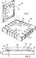
- a chip 11 of semiconductor material for example, silicon
- a surface covered by a layer 12 of insulating material for example, silicon dioxide.
- Substantially coplanar metal pads 13 which are the ends of the electrical connections to the active portions of the electronic device, appear on the surface 12 and are surmounted by bumps 14 of soldering material, for example, an alloy of lead and tin.
- the device 10 is ready to be mounted on a flat mounting substrate 20 of insulating, for example, ceramic material on which there are metal tracks 21 which terminate, on the upper surface of the substrate 20, in areas 22 arranged in the same configuration as the pads 13 of the device 10.
- the metal tracks 21 in this example extend over the edges of the substrate 20 in order to be soldered to a printed circuit board, not shown.
- the substrate could itself be a printed circuit board.
- the mounting substrate could have interconnection elements which extend through its entire thickness and terminate in contact areas on both of its faces.
- Figure 2 shows the device 10 on the mounting substrate 20 after the pads 13 have been soldered to the terminal areas 22 of the metal tracks 21 by means of the soldering material of the bumps 14.
- the pads 13 are the end surfaces of metal interconnection elements which extend through the insulating layer 12 from contact areas of the chip 11 of semiconductor material to the surface of the layer 12.
- some of the interconnection elements may not be in contact with areas of the chip but with contact areas of electrically-conductive elements electrically insulated from the chip, for example, gate electrodes or capacitor electrodes.
- the next manufacturing step consists of the application of a drop 25 of thermosetting resin, for example, an epoxy resin, which may be filled with grains of silica to increase its thermal conductivity, and which flows into the space 26 between the opposed surfaces of the device 20 and of the substrate 20 and encloses the entire chip, sealing it on the substrate and insulating it from the outside environment.
- thermosetting resin for example, an epoxy resin, which may be filled with grains of silica to increase its thermal conductivity
- the semiconductor device according to the invention has a metal plate 30 extending over the layer of insulating material 12.
- the plate 30 is partially incorporated in the layer of insulating material 12 so as to have an extensive uncovered surface substantially coplanar with the pads 13.
- the plate 30 is arranged in the region of a power component of the electronic device formed in the chip 11 and may be formed by the same steps of the manufacturing process by which the metal connections which terminate on the surface in the pads 13 are formed. Moreover, it may be completely insulated from the surface of the chip 12 of semiconductor material, or it may be in contact with a predetermined area thereof. In this latter case, the plate 30 constitutes a terminal of the device.
- Bumps 31 similar to those, indicated 14, formed on the pads 13, are formed on the plate 30.
- the bumps 14 and 31 can be formed simultaneously and by the same manufacturing steps, for example, by a galvanic deposition (electroplating) process.
- a screen printing process it is advantageous to form a single element of soldering material on the plate 30, that is, a layer of soldering material over its entire surface.
- the mounting substrate 20 of Figure 3 differs from that of Figure 1 in that it contains a metal element 35 which has a relatively extensive surface, to which the plate 30 of the device 10 is soldered, as shown in Figure 4.
- the metal element 35 extends through the entire thickness of the mounting substrate 20 and can be put into contact with an external heat sink, not shown, by means of its opposite surface to that which is soldered to the device 10. With this structure, it is possible to achieve very efficient dissipation of the heat generated by the semiconductor device in operation.
- the metal element 35 may have a different structure, for example, it could extend only on the surface of the substrate 20 without extending through it. In any case, the efficiency of the heat dissipation is much greater than that which can be achieved by the known technique, by virtue of the low thermal resistance of the metal contacts and the relatively large extent of the contacting metal surfaces.
Landscapes
- Wire Bonding (AREA)
- Cooling Or The Like Of Semiconductors Or Solid State Devices (AREA)
Priority Applications (3)
| Application Number | Priority Date | Filing Date | Title |
|---|---|---|---|
| DE69840823T DE69840823D1 (de) | 1998-03-10 | 1998-03-10 | Leistungshalbleiteranordnung für Flipchipverbindungen |
| EP98830132A EP0942635B1 (fr) | 1998-03-10 | 1998-03-10 | Dispositif semiconducteur de puissance pour une connexion du type "flip-chip" |
| US09/237,407 US6291893B1 (en) | 1998-03-10 | 1999-01-26 | Power semiconductor device for “flip-chip” connections |
Applications Claiming Priority (1)
| Application Number | Priority Date | Filing Date | Title |
|---|---|---|---|
| EP98830132A EP0942635B1 (fr) | 1998-03-10 | 1998-03-10 | Dispositif semiconducteur de puissance pour une connexion du type "flip-chip" |
Publications (2)
| Publication Number | Publication Date |
|---|---|
| EP0942635A1 true EP0942635A1 (fr) | 1999-09-15 |
| EP0942635B1 EP0942635B1 (fr) | 2009-05-13 |
Family
ID=8236568
Family Applications (1)
| Application Number | Title | Priority Date | Filing Date |
|---|---|---|---|
| EP98830132A Expired - Lifetime EP0942635B1 (fr) | 1998-03-10 | 1998-03-10 | Dispositif semiconducteur de puissance pour une connexion du type "flip-chip" |
Country Status (3)
| Country | Link |
|---|---|
| US (1) | US6291893B1 (fr) |
| EP (1) | EP0942635B1 (fr) |
| DE (1) | DE69840823D1 (fr) |
Families Citing this family (5)
| Publication number | Priority date | Publication date | Assignee | Title |
|---|---|---|---|---|
| DE19940564C2 (de) * | 1999-08-26 | 2002-03-21 | Infineon Technologies Ag | Chipkartenmodul und diesen umfassende Chipkarte, sowie Verfahren zur Herstellung des Chipkartenmoduls |
| US6583513B1 (en) * | 1999-10-12 | 2003-06-24 | Agilent Technologies, Inc. | Integrated circuit package with an IC chip and pads that dissipate heat away from the chip |
| US20050286234A1 (en) * | 2004-06-29 | 2005-12-29 | International Business Machines Corporation | Thermally conductive composite interface and methods of fabrication thereof for an electronic assembly |
| US9039427B2 (en) * | 2013-02-14 | 2015-05-26 | Texas Instruments Incorporated | Interdigitated chip capacitor assembly |
| CN108231698A (zh) * | 2017-12-29 | 2018-06-29 | 中国电子科技集团公司第十三研究所 | 陶瓷焊盘阵列外壳 |
Citations (4)
| Publication number | Priority date | Publication date | Assignee | Title |
|---|---|---|---|---|
| JPS62144346A (ja) * | 1985-12-19 | 1987-06-27 | Matsushita Electric Ind Co Ltd | 半導体集積回路素子 |
| JPH0661304A (ja) * | 1992-08-06 | 1994-03-04 | Nec Corp | 半導体素子のボンディング方法 |
| EP0600590A1 (fr) * | 1992-12-03 | 1994-06-08 | International Computers Limited | Refroidissement de circuits électroniques assemblés |
| EP0637078A1 (fr) * | 1993-07-29 | 1995-02-01 | Motorola, Inc. | Un dispositif semi-conducteur avec dissipation de chaleur améliorée |
Family Cites Families (2)
| Publication number | Priority date | Publication date | Assignee | Title |
|---|---|---|---|---|
| JP2679681B2 (ja) * | 1995-04-28 | 1997-11-19 | 日本電気株式会社 | 半導体装置、半導体装置用パッケージ及びその製造方法 |
| US5977626A (en) * | 1998-08-12 | 1999-11-02 | Industrial Technology Research Institute | Thermally and electrically enhanced PBGA package |
-
1998
- 1998-03-10 DE DE69840823T patent/DE69840823D1/de not_active Expired - Lifetime
- 1998-03-10 EP EP98830132A patent/EP0942635B1/fr not_active Expired - Lifetime
-
1999
- 1999-01-26 US US09/237,407 patent/US6291893B1/en not_active Expired - Lifetime
Patent Citations (4)
| Publication number | Priority date | Publication date | Assignee | Title |
|---|---|---|---|---|
| JPS62144346A (ja) * | 1985-12-19 | 1987-06-27 | Matsushita Electric Ind Co Ltd | 半導体集積回路素子 |
| JPH0661304A (ja) * | 1992-08-06 | 1994-03-04 | Nec Corp | 半導体素子のボンディング方法 |
| EP0600590A1 (fr) * | 1992-12-03 | 1994-06-08 | International Computers Limited | Refroidissement de circuits électroniques assemblés |
| EP0637078A1 (fr) * | 1993-07-29 | 1995-02-01 | Motorola, Inc. | Un dispositif semi-conducteur avec dissipation de chaleur améliorée |
Non-Patent Citations (2)
| Title |
|---|
| PATENT ABSTRACTS OF JAPAN vol. 011, no. 376 (E - 563) 8 December 1987 (1987-12-08) * |
| PATENT ABSTRACTS OF JAPAN vol. 018, no. 299 (E - 1558) 8 June 1994 (1994-06-08) * |
Also Published As
| Publication number | Publication date |
|---|---|
| DE69840823D1 (de) | 2009-06-25 |
| US6291893B1 (en) | 2001-09-18 |
| EP0942635B1 (fr) | 2009-05-13 |
Similar Documents
| Publication | Publication Date | Title |
|---|---|---|
| JP2751912B2 (ja) | 半導体装置およびその製造方法 | |
| EP0594395B1 (fr) | Module semi-conducteur de puissance | |
| US8564049B2 (en) | Flip chip contact (FCC) power package | |
| KR100363776B1 (ko) | 리드와 직접 접속된 집적회로 칩 패키지 | |
| CN101145546B (zh) | 半导体器件及其制造方法 | |
| JPH09260552A (ja) | 半導体チップの実装構造 | |
| US20060145319A1 (en) | Flip chip contact (FCC) power package | |
| JPH10163386A (ja) | 半導体装置、半導体パッケージおよび実装回路装置 | |
| JP2001015679A (ja) | 半導体装置及びその製造方法 | |
| US6841865B2 (en) | Semiconductor device having clips for connecting to external elements | |
| JP2001298115A (ja) | 半導体装置及びその製造方法、回路基板並びに電子機器 | |
| JP2005064479A (ja) | 回路モジュール | |
| EP1466357A1 (fr) | Enveloppe montee sur une surface avec fond de plaquette espace de la carte de support | |
| EP0942635B1 (fr) | Dispositif semiconducteur de puissance pour une connexion du type "flip-chip" | |
| US9337132B2 (en) | Methods and configuration for manufacturing flip chip contact (FCC) power package | |
| JPH09326450A (ja) | 半導体装置およびその製造方法 | |
| JPH08148647A (ja) | 半導体装置 | |
| JPH11297752A (ja) | 半導体チップの実装構造、およびこの実装構造を有する半導体装置 | |
| US6963129B1 (en) | Multi-chip package having a contiguous heat spreader assembly | |
| JP3297959B2 (ja) | 半導体装置 | |
| JP3065288B2 (ja) | 半導体ベアチップの封止方法、半導体集積回路装置、および半導体集積回路装置の製造方法 | |
| JPS63284831A (ja) | 混成集積回路の製造方法 | |
| JPH11251497A (ja) | 電子回路モジュール | |
| JPH0773110B2 (ja) | 半導体集積回路装置 | |
| JP2001118951A (ja) | 半導体装置 |
Legal Events
| Date | Code | Title | Description |
|---|---|---|---|
| PUAI | Public reference made under article 153(3) epc to a published international application that has entered the european phase |
Free format text: ORIGINAL CODE: 0009012 |
|
| AK | Designated contracting states |
Kind code of ref document: A1 Designated state(s): DE FR GB IT |
|
| AX | Request for extension of the european patent |
Free format text: AL;LT;LV;MK;RO;SI |
|
| 17P | Request for examination filed |
Effective date: 20000310 |
|
| AKX | Designation fees paid |
Free format text: DE FR GB IT |
|
| 17Q | First examination report despatched |
Effective date: 20061027 |
|
| GRAP | Despatch of communication of intention to grant a patent |
Free format text: ORIGINAL CODE: EPIDOSNIGR1 |
|
| GRAS | Grant fee paid |
Free format text: ORIGINAL CODE: EPIDOSNIGR3 |
|
| GRAA | (expected) grant |
Free format text: ORIGINAL CODE: 0009210 |
|
| AK | Designated contracting states |
Kind code of ref document: B1 Designated state(s): DE FR GB IT |
|
| REG | Reference to a national code |
Ref country code: GB Ref legal event code: FG4D |
|
| REF | Corresponds to: |
Ref document number: 69840823 Country of ref document: DE Date of ref document: 20090625 Kind code of ref document: P |
|
| PLBE | No opposition filed within time limit |
Free format text: ORIGINAL CODE: 0009261 |
|
| STAA | Information on the status of an ep patent application or granted ep patent |
Free format text: STATUS: NO OPPOSITION FILED WITHIN TIME LIMIT |
|
| RAP2 | Party data changed (patent owner data changed or rights of a patent transferred) |
Owner name: STMICROELECTRONICS SRL |
|
| 26N | No opposition filed |
Effective date: 20100216 |
|
| PGFP | Annual fee paid to national office [announced via postgrant information from national office to epo] |
Ref country code: GB Payment date: 20130228 Year of fee payment: 16 |
|
| PGFP | Annual fee paid to national office [announced via postgrant information from national office to epo] |
Ref country code: FR Payment date: 20130429 Year of fee payment: 16 |
|
| GBPC | Gb: european patent ceased through non-payment of renewal fee |
Effective date: 20140310 |
|
| REG | Reference to a national code |
Ref country code: FR Ref legal event code: ST Effective date: 20141128 |
|
| PG25 | Lapsed in a contracting state [announced via postgrant information from national office to epo] |
Ref country code: GB Free format text: LAPSE BECAUSE OF NON-PAYMENT OF DUE FEES Effective date: 20140310 Ref country code: FR Free format text: LAPSE BECAUSE OF NON-PAYMENT OF DUE FEES Effective date: 20140331 |
|
| PGFP | Annual fee paid to national office [announced via postgrant information from national office to epo] |
Ref country code: DE Payment date: 20170222 Year of fee payment: 20 |
|
| PGFP | Annual fee paid to national office [announced via postgrant information from national office to epo] |
Ref country code: IT Payment date: 20170221 Year of fee payment: 20 |
|
| REG | Reference to a national code |
Ref country code: DE Ref legal event code: R071 Ref document number: 69840823 Country of ref document: DE |