EP0944162A1 - Selbstsynchronisierender Gleichstromwandler und Verfahren zu dessen Betrieb - Google Patents
Selbstsynchronisierender Gleichstromwandler und Verfahren zu dessen Betrieb Download PDFInfo
- Publication number
- EP0944162A1 EP0944162A1 EP98400651A EP98400651A EP0944162A1 EP 0944162 A1 EP0944162 A1 EP 0944162A1 EP 98400651 A EP98400651 A EP 98400651A EP 98400651 A EP98400651 A EP 98400651A EP 0944162 A1 EP0944162 A1 EP 0944162A1
- Authority
- EP
- European Patent Office
- Prior art keywords
- buck
- push
- pull
- pulse
- converter
- Prior art date
- Legal status (The legal status is an assumption and is not a legal conclusion. Google has not performed a legal analysis and makes no representation as to the accuracy of the status listed.)
- Granted
Links
- 238000000034 method Methods 0.000 title claims description 4
- 238000005070 sampling Methods 0.000 claims 2
- 238000010586 diagram Methods 0.000 description 5
- 230000010363 phase shift Effects 0.000 description 3
- 230000003247 decreasing effect Effects 0.000 description 1
- 230000001419 dependent effect Effects 0.000 description 1
- 230000000694 effects Effects 0.000 description 1
- 238000009532 heart rate measurement Methods 0.000 description 1
- 238000005259 measurement Methods 0.000 description 1
- 238000012986 modification Methods 0.000 description 1
- 230000004048 modification Effects 0.000 description 1
- 239000004065 semiconductor Substances 0.000 description 1
Images

Classifications
-
- H—ELECTRICITY
- H02—GENERATION; CONVERSION OR DISTRIBUTION OF ELECTRIC POWER
- H02M—APPARATUS FOR CONVERSION BETWEEN AC AND AC, BETWEEN AC AND DC, OR BETWEEN DC AND DC, AND FOR USE WITH MAINS OR SIMILAR POWER SUPPLY SYSTEMS; CONVERSION OF DC OR AC INPUT POWER INTO SURGE OUTPUT POWER; CONTROL OR REGULATION THEREOF
- H02M3/00—Conversion of DC power input into DC power output
- H02M3/22—Conversion of DC power input into DC power output with intermediate conversion into AC
- H02M3/24—Conversion of DC power input into DC power output with intermediate conversion into AC by static converters
- H02M3/28—Conversion of DC power input into DC power output with intermediate conversion into AC by static converters using discharge tubes with control electrode or semiconductor devices with control electrode to produce the intermediate AC
- H02M3/325—Conversion of DC power input into DC power output with intermediate conversion into AC by static converters using discharge tubes with control electrode or semiconductor devices with control electrode to produce the intermediate AC using devices of a triode or a transistor type requiring continuous application of a control signal
- H02M3/335—Conversion of DC power input into DC power output with intermediate conversion into AC by static converters using discharge tubes with control electrode or semiconductor devices with control electrode to produce the intermediate AC using devices of a triode or a transistor type requiring continuous application of a control signal using semiconductor devices only
- H02M3/337—Conversion of DC power input into DC power output with intermediate conversion into AC by static converters using discharge tubes with control electrode or semiconductor devices with control electrode to produce the intermediate AC using devices of a triode or a transistor type requiring continuous application of a control signal using semiconductor devices only in push-pull configuration
- H02M3/3372—Conversion of DC power input into DC power output with intermediate conversion into AC by static converters using discharge tubes with control electrode or semiconductor devices with control electrode to produce the intermediate AC using devices of a triode or a transistor type requiring continuous application of a control signal using semiconductor devices only in push-pull configuration of the parallel type
- H02M3/3374—Conversion of DC power input into DC power output with intermediate conversion into AC by static converters using discharge tubes with control electrode or semiconductor devices with control electrode to produce the intermediate AC using devices of a triode or a transistor type requiring continuous application of a control signal using semiconductor devices only in push-pull configuration of the parallel type with preregulator, e.g. current injected push-pull
-
- Y—GENERAL TAGGING OF NEW TECHNOLOGICAL DEVELOPMENTS; GENERAL TAGGING OF CROSS-SECTIONAL TECHNOLOGIES SPANNING OVER SEVERAL SECTIONS OF THE IPC; TECHNICAL SUBJECTS COVERED BY FORMER USPC CROSS-REFERENCE ART COLLECTIONS [XRACs] AND DIGESTS
- Y02—TECHNOLOGIES OR APPLICATIONS FOR MITIGATION OR ADAPTATION AGAINST CLIMATE CHANGE
- Y02B—CLIMATE CHANGE MITIGATION TECHNOLOGIES RELATED TO BUILDINGS, e.g. HOUSING, HOUSE APPLIANCES OR RELATED END-USER APPLICATIONS
- Y02B70/00—Technologies for an efficient end-user side electric power management and consumption
- Y02B70/10—Technologies improving the efficiency by using switched-mode power supplies [SMPS], i.e. efficient power electronics conversion e.g. power factor correction or reduction of losses in power supplies or efficient standby modes
Definitions
- the present invention relates to a DC/DC converter adapted to convert an unstable DC input voltage into a high DC output voltage.
- a conventional DC/DC converter comprises as input stage, a first switching circuit operating as a current source and, as output stage, a second switching circuit operating to increase the voltage.
- a first switching circuit operating as a current source
- a second switching circuit operating to increase the voltage.
- the basic idea behind the present invention is that the optimal regulation is not constant but is dependent on the input voltage value and that the optimal regulation is obtained for a phase shift of about 180 degrees between the output voltage of the input stage and the output voltage of the output stage.
- the invention provides a DC/DC converter and a method of synchronizing same as defined in the appended claims.
- a DC/DC converter comprises a buck stage that includes a buck switch, a push-pull stage that includes push-pull switches, a controller to control the switching phases of the buck and push-pull switches, and an autosynchronizing circuit adapted to produce synchronization pulses at a fixed frequency and to automatically and continuously adjust the turn-on phases of the buck and push-pull switches to an optimal value at each occurrence of a synchronization pulse.
- the optimal value for the relative phase shift is automatically obtained at the start-up of the converter and is then continuously adjusted during the operation thereof.
- a high output voltage (several thousands of volts) can be obtained and can be maintained constant even for relatively high fluctuations of the input DC voltage, e.g. fluctuations of between 30 and 50 volts.
- a diagram of a quasi-resonant DC/DC converter incorporating the invention The input stage is a buck circuit 11, the input terminals of which accept the input bus voltage V IN .
- the buck circuit is a topology providing an output voltage V BUCK that is always lower or equal to the input voltage.
- the buck circuit operates in a continuous mode (i.e. the inductance current never falls to zero) and switches at a fixed frequency controlled by drive pulses T BUCK applied to the buck switch 12.
- the output stage of the DC/DC converter is a resonant push-pull circuit 13 having two legs 13A and 13B including switches 14A and 14B respectively, that are caused to switch at a fixed frequency to drive a high voltage transformer 15.
- the drive pulses T BUCK are produced by a PWM controller 17, the purpose of which is to regulate the buck output voltage V BUCK for a given bus input voltage range.
- the controller may be for instance a UC 1846 J circuit manufactured by UNITRODETM at 7, Continental Boulevard, Merrimack, NH 03054 - USA).
- the regulation is based on the signals from two regulation loops embodied in feedback network 16 adapted to provide signals representative of both the buck output voltage V BUCK and the buck inductance current I BUCK .
- the buck output voltage V BUCK is compared to a reference value V REF and the output current I BUCK is used to control the output voltage in order to allow same to reach the correct value.
- the controller 17 is adapted to control the duration of the drive pulses T BUCK so that the output voltage V BUCK reaches the correct value.
- the drive pulse T BUCK is turned off, whereby the energy transfer to the push-pull stage 15 is temporarily stopped until the next switching period.
- the controller internal logic toggles under the control of a synchronization pulse T SYNC in order to deliver the drive pulse T BUCK to its output A or its output B, which drive pulse T BUCK is sent to the buck switch 12 through a digital OR-gate 18A, for instance a 54 AC 32 circuit, in series with an opto-coupler 20, that is for instance a HCPL 5601 circuit.
- the circuit 54 AC 32 is manufactured by NATIONAL SEMICONDUCTORTM at 2900 Semiconductor Drive, Santa Clara, California 95052-8090 - USA, whilst the circuit HCPL 5601 is manufactured by the HEWLETT PACKARDTM COMPANY at 370, West Trimble Road, San Jose, California 95131 - USA.
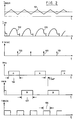
- the synchronization pulses are produced at a fixed frequency by an autosynchronization circuit 19, the operation of which is set forth herein after with further reference to the time diagrams in Fig. 2.
- waveform 101 represents the inductance current in the buck stage
- waveforms 102 represent the current in the push-pull stage
- the arrows 103 represent the synchronization pulse occurrences
- time span 104 represents the turn-on phase of the switch in leg A of the push-pull stage
- time span 105 represents the turn-on phase of the switch in push-pull leg B
- time span 106 represents the turn-on phase of the drive pulse T BUCK for the buck switch.
- the autosynchronization circuit is for instance a package of the type SMC 610 A, that is an ASIC based on the CMOS 1 ⁇ m technology, manufactured by MATRATM MHS S.A. at La Chantrerie - Rue de Gachet, BP 70602, F-44306 France Cedex 03, France.
- the purpose of the autosynchronization circuit in this invention is to cause each gap time T GAP between the turn-on phases Ai and Bi of the push-pull legs to be centered on the middle of each drive pulse T BUCK , thereby to make the regulation capability of the converter independent from the fluctuations of the input voltage V IN .
- the autosynchronization circuit 19 controls the turn-on phase of the push-pull switches 14A and 14B from the buck phase and from the width of the drive pulses T BUCK .
- the autosynchronization circuit 19 starts the width pulse measurement of the pulse T BUCK .
- the period of the synchronization pulse T SYNC is determined by an oscillator related to the values of RL and CL (clock-low).
- the pulse width measurement depends on a high frequency oscillator related to RH and CH (Clock-High).
- the time during which T BUCK is ON is measured using an internal digital counter. Two microseconds or so after the starting point of T SYNC, the drive pulse T BUCK is sampled.
- T BUCK is declared to be OFF. If it is a high logical level, the internal counter starts to count the number N of clock high periods till it falls to a low logical level.
- the width of T BUCK is measured once for two periods of the buck switching frequency, i.e. two periods of the synchronization pulse T SYNC .
- the autosynchronization circuit 19 When the autosynchronization circuit 19 detects the end of the pulse T BUCK , it terminates its internal pulse width counting.
- the value of the counter divided by 2 (one shift to the right) is added to the turn-on phase of the synchronization pulse T SYNC during two periods in order to give the turn-on points of the push-pull switches 14A and 14B, that is the starting points of the command signals CLK-PPA and CLK-PPB for the push-pull legs A and B respectively.
- the autosynchronization circuit 19 automatically and continuously determines the middle point of the drive pulse T BUCK and continuously adjusts the relative phase shift to the optimal value for the effective value of the input voltage.
Landscapes
- Engineering & Computer Science (AREA)
- Power Engineering (AREA)
- Dc-Dc Converters (AREA)
Priority Applications (4)
| Application Number | Priority Date | Filing Date | Title |
|---|---|---|---|
| EP98400651A EP0944162B1 (de) | 1998-03-19 | 1998-03-19 | Selbstsynchronisierender Gleichstromwandler und Verfahren zu dessen Betrieb |
| DE69840566T DE69840566D1 (de) | 1998-03-19 | 1998-03-19 | Selbstsynchronisierender Gleichstromwandler und Verfahren zu dessen Betrieb |
| JP11069847A JP2000125550A (ja) | 1998-03-19 | 1999-03-16 | 自動同期dc/dcコンバ―タおよびその作動方法 |
| US09/270,511 US6141225A (en) | 1998-03-19 | 1999-03-17 | Auto-synchronized DC/DC converter and method of operating same |
Applications Claiming Priority (1)
| Application Number | Priority Date | Filing Date | Title |
|---|---|---|---|
| EP98400651A EP0944162B1 (de) | 1998-03-19 | 1998-03-19 | Selbstsynchronisierender Gleichstromwandler und Verfahren zu dessen Betrieb |
Publications (2)
| Publication Number | Publication Date |
|---|---|
| EP0944162A1 true EP0944162A1 (de) | 1999-09-22 |
| EP0944162B1 EP0944162B1 (de) | 2009-02-18 |
Family
ID=8235304
Family Applications (1)
| Application Number | Title | Priority Date | Filing Date |
|---|---|---|---|
| EP98400651A Expired - Lifetime EP0944162B1 (de) | 1998-03-19 | 1998-03-19 | Selbstsynchronisierender Gleichstromwandler und Verfahren zu dessen Betrieb |
Country Status (4)
| Country | Link |
|---|---|
| US (1) | US6141225A (de) |
| EP (1) | EP0944162B1 (de) |
| JP (1) | JP2000125550A (de) |
| DE (1) | DE69840566D1 (de) |
Cited By (5)
| Publication number | Priority date | Publication date | Assignee | Title |
|---|---|---|---|---|
| WO2001037411A3 (en) * | 1999-11-19 | 2001-11-01 | Iwatt | Isolated power converter having primary feedback control |
| US6381150B2 (en) | 1999-11-19 | 2002-04-30 | Iwatt | Isolated dual converter having primary side internal feedback for output regulation |
| US7558083B2 (en) | 1997-01-24 | 2009-07-07 | Synqor, Inc. | High efficiency power converter |
| US7564702B2 (en) | 1997-01-24 | 2009-07-21 | Synqor, Inc. | High efficiency power converter |
| US10199950B1 (en) | 2013-07-02 | 2019-02-05 | Vlt, Inc. | Power distribution architecture with series-connected bus converter |
Families Citing this family (9)
| Publication number | Priority date | Publication date | Assignee | Title |
|---|---|---|---|---|
| AU2003220665A1 (en) * | 2002-04-03 | 2003-10-20 | International Rectifier Corporation | Synchronous buck converter improvements |
| US7477529B2 (en) * | 2002-11-01 | 2009-01-13 | Honeywell International Inc. | High-voltage power supply |
| KR100678945B1 (ko) * | 2004-12-03 | 2007-02-07 | 삼성전자주식회사 | 터치패드 입력 정보 처리 장치 및 방법 |
| KR100597415B1 (ko) | 2004-12-16 | 2006-07-05 | 삼성전자주식회사 | 가변저항 조절에 의해 개선된 스위칭 동작을 수행하는동기 정류형 직류/직류 컨버터 |
| JP5090202B2 (ja) | 2008-02-19 | 2012-12-05 | 株式会社リコー | 電源回路 |
| KR101022772B1 (ko) * | 2008-12-30 | 2011-03-17 | 한국전기연구원 | 연료전지용 전력변환장치. |
| TW201312916A (zh) | 2011-09-15 | 2013-03-16 | Richtek Technology Corp | 電源供應電路及具有適應性致能電荷泵之電源供應電路 |
| US9647572B2 (en) | 2011-11-10 | 2017-05-09 | Powerbyproxi Limited | Method for controlling a converter |
| WO2018048312A1 (en) | 2016-09-06 | 2018-03-15 | Powerbyproxi Limited | An inductive power transmitter |
Citations (2)
| Publication number | Priority date | Publication date | Assignee | Title |
|---|---|---|---|---|
| US4656570A (en) * | 1985-09-23 | 1987-04-07 | Pioneer Magnetics, Inc. | Self-balancing push-pull square wave converter type of switched power supply |
| EP0613233A1 (de) * | 1993-02-26 | 1994-08-31 | Siemens Nixdorf Informationssysteme Aktiengesellschaft | Schaltungsanordnung zum Ansteuern der Schaltglieder eines Auf-Abwärts-Spannungswandlers |
Family Cites Families (6)
| Publication number | Priority date | Publication date | Assignee | Title |
|---|---|---|---|---|
| US4953068A (en) * | 1989-11-08 | 1990-08-28 | Unisys Corporation | Full bridge power converter with multiple zero voltage resonant transition switching |
| FR2663169A1 (fr) * | 1990-06-08 | 1991-12-13 | Alcatel Espace | Dispositif de regulation d'un parametre par une structure bidirectionnelle en courant. |
| GB9206022D0 (en) * | 1992-03-19 | 1992-04-29 | Astec Int Ltd | Push-pull inverter |
| US5430641A (en) * | 1992-04-27 | 1995-07-04 | Dell Usa, L.P. | Synchronously switching inverter and regulator |
| US5481178A (en) * | 1993-03-23 | 1996-01-02 | Linear Technology Corporation | Control circuit and method for maintaining high efficiency over broad current ranges in a switching regulator circuit |
| US5844378A (en) * | 1995-01-25 | 1998-12-01 | Micro Linear Corp | High side driver technique for miniature cold cathode fluorescent lamp system |
-
1998
- 1998-03-19 EP EP98400651A patent/EP0944162B1/de not_active Expired - Lifetime
- 1998-03-19 DE DE69840566T patent/DE69840566D1/de not_active Expired - Lifetime
-
1999
- 1999-03-16 JP JP11069847A patent/JP2000125550A/ja active Pending
- 1999-03-17 US US09/270,511 patent/US6141225A/en not_active Expired - Fee Related
Patent Citations (2)
| Publication number | Priority date | Publication date | Assignee | Title |
|---|---|---|---|---|
| US4656570A (en) * | 1985-09-23 | 1987-04-07 | Pioneer Magnetics, Inc. | Self-balancing push-pull square wave converter type of switched power supply |
| EP0613233A1 (de) * | 1993-02-26 | 1994-08-31 | Siemens Nixdorf Informationssysteme Aktiengesellschaft | Schaltungsanordnung zum Ansteuern der Schaltglieder eines Auf-Abwärts-Spannungswandlers |
Cited By (13)
| Publication number | Priority date | Publication date | Assignee | Title |
|---|---|---|---|---|
| US8493751B2 (en) | 1997-01-24 | 2013-07-23 | Synqor, Inc. | High efficiency power converter |
| US7558083B2 (en) | 1997-01-24 | 2009-07-07 | Synqor, Inc. | High efficiency power converter |
| US7564702B2 (en) | 1997-01-24 | 2009-07-21 | Synqor, Inc. | High efficiency power converter |
| US8023290B2 (en) | 1997-01-24 | 2011-09-20 | Synqor, Inc. | High efficiency power converter |
| US9143042B2 (en) | 1997-01-24 | 2015-09-22 | Synqor, Inc. | High efficiency power converter |
| US6370039B1 (en) | 1999-11-19 | 2002-04-09 | Iwatt | Isolated power converter having primary feedback control |
| US6381150B2 (en) | 1999-11-19 | 2002-04-30 | Iwatt | Isolated dual converter having primary side internal feedback for output regulation |
| WO2001037411A3 (en) * | 1999-11-19 | 2001-11-01 | Iwatt | Isolated power converter having primary feedback control |
| US10199950B1 (en) | 2013-07-02 | 2019-02-05 | Vlt, Inc. | Power distribution architecture with series-connected bus converter |
| US10594223B1 (en) | 2013-07-02 | 2020-03-17 | Vlt, Inc. | Power distribution architecture with series-connected bus converter |
| US11075583B1 (en) | 2013-07-02 | 2021-07-27 | Vicor Corporation | Power distribution architecture with series-connected bus converter |
| US11705820B2 (en) | 2013-07-02 | 2023-07-18 | Vicor Corporation | Power distribution architecture with series-connected bus converter |
| US12395087B1 (en) | 2013-07-02 | 2025-08-19 | Vicor Corporation | Power distribution architecture with series-connected bus converter |
Also Published As
| Publication number | Publication date |
|---|---|
| EP0944162B1 (de) | 2009-02-18 |
| DE69840566D1 (de) | 2009-04-02 |
| JP2000125550A (ja) | 2000-04-28 |
| US6141225A (en) | 2000-10-31 |
Similar Documents
| Publication | Publication Date | Title |
|---|---|---|
| US7161816B2 (en) | System and method for input current shaping in a power converter | |
| EP0944162B1 (de) | Selbstsynchronisierender Gleichstromwandler und Verfahren zu dessen Betrieb | |
| KR102225011B1 (ko) | 공진형 변환기들에서의 버스트 모드 제어 | |
| US5734564A (en) | High-efficiency switching power converter | |
| CN105305783B (zh) | 用于谐振转换器的控制设备 | |
| US9190909B2 (en) | Control device for multiphase interleaved DC-DC converter and control method thereof | |
| US20200403497A1 (en) | Control circuit and method of a switching power supply | |
| CN111327196B (zh) | 在功率转换器中同步多个控制器 | |
| CN103098358A (zh) | 使用双极结型晶体管的自激振荡变流器的调节控制器 | |
| KR0154818B1 (ko) | 공진형 콘버터 제어 시스템 | |
| US5402330A (en) | Switch mode power supply with reduced input current distortion | |
| CN119483231B (zh) | 软启动控制电路及方法、谐振变换控制电路、电子设备 | |
| CN111431424B (zh) | 一种谐振电路 | |
| JP3572601B2 (ja) | 電圧共振型スイッチング電源及び電圧共振型スイッチング電源の制御方法 | |
| JPH067742B2 (ja) | Dc―dcコンバータ | |
| JP3191756B2 (ja) | スイッチング電源装置 | |
| JP2976638B2 (ja) | スイッチング電源 | |
| JPH05211766A (ja) | 高デューティサイクル電流制御型pwmレギュレータの安定性を改善する回路 | |
| JP2623642B2 (ja) | 電圧共振型スイッチング電源の同期発生回路 | |
| US20250211100A1 (en) | Conversion control circuit for controlling a resonant power converter and control method thereof | |
| WO1989005057A1 (en) | High frequency rectifier with sinusshaped primary current | |
| JPH07147780A (ja) | 電源装置 | |
| JPH04308459A (ja) | 電源装置 | |
| CN120262892A (zh) | 一种软启动控制方法、控制装置及开关电源 | |
| JPH07163144A (ja) | 多入力dc−dcコンバータ装置 |
Legal Events
| Date | Code | Title | Description |
|---|---|---|---|
| PUAI | Public reference made under article 153(3) epc to a published international application that has entered the european phase |
Free format text: ORIGINAL CODE: 0009012 |
|
| AK | Designated contracting states |
Kind code of ref document: A1 Designated state(s): DE FR GB IT |
|
| AX | Request for extension of the european patent |
Free format text: AL;LT;LV;MK;RO;SI |
|
| 17P | Request for examination filed |
Effective date: 20000322 |
|
| AKX | Designation fees paid |
Free format text: DE FR GB IT |
|
| RAP1 | Party data changed (applicant data changed or rights of an application transferred) |
Owner name: ALCATEL LUCENT |
|
| 17Q | First examination report despatched |
Effective date: 20071228 |
|
| GRAP | Despatch of communication of intention to grant a patent |
Free format text: ORIGINAL CODE: EPIDOSNIGR1 |
|
| GRAS | Grant fee paid |
Free format text: ORIGINAL CODE: EPIDOSNIGR3 |
|
| GRAA | (expected) grant |
Free format text: ORIGINAL CODE: 0009210 |
|
| GRAL | Information related to payment of fee for publishing/printing deleted |
Free format text: ORIGINAL CODE: EPIDOSDIGR3 |
|
| GRAS | Grant fee paid |
Free format text: ORIGINAL CODE: EPIDOSNIGR3 |
|
| AK | Designated contracting states |
Kind code of ref document: B1 Designated state(s): DE FR GB IT |
|
| REG | Reference to a national code |
Ref country code: GB Ref legal event code: FG4D |
|
| REF | Corresponds to: |
Ref document number: 69840566 Country of ref document: DE Date of ref document: 20090402 Kind code of ref document: P |
|
| PLBE | No opposition filed within time limit |
Free format text: ORIGINAL CODE: 0009261 |
|
| STAA | Information on the status of an ep patent application or granted ep patent |
Free format text: STATUS: NO OPPOSITION FILED WITHIN TIME LIMIT |
|
| 26N | No opposition filed |
Effective date: 20091119 |
|
| REG | Reference to a national code |
Ref country code: FR Ref legal event code: CA Effective date: 20150521 |
|
| REG | Reference to a national code |
Ref country code: FR Ref legal event code: CA Effective date: 20150521 |
|
| REG | Reference to a national code |
Ref country code: FR Ref legal event code: PLFP Year of fee payment: 19 |
|
| PGFP | Annual fee paid to national office [announced via postgrant information from national office to epo] |
Ref country code: DE Payment date: 20160315 Year of fee payment: 19 |
|
| PGFP | Annual fee paid to national office [announced via postgrant information from national office to epo] |
Ref country code: GB Payment date: 20160316 Year of fee payment: 19 Ref country code: FR Payment date: 20160223 Year of fee payment: 19 |
|
| PGFP | Annual fee paid to national office [announced via postgrant information from national office to epo] |
Ref country code: IT Payment date: 20160324 Year of fee payment: 19 |
|
| REG | Reference to a national code |
Ref country code: DE Ref legal event code: R119 Ref document number: 69840566 Country of ref document: DE |
|
| GBPC | Gb: european patent ceased through non-payment of renewal fee |
Effective date: 20170319 |
|
| REG | Reference to a national code |
Ref country code: FR Ref legal event code: ST Effective date: 20171130 |
|
| PG25 | Lapsed in a contracting state [announced via postgrant information from national office to epo] |
Ref country code: DE Free format text: LAPSE BECAUSE OF NON-PAYMENT OF DUE FEES Effective date: 20171003 Ref country code: FR Free format text: LAPSE BECAUSE OF NON-PAYMENT OF DUE FEES Effective date: 20170331 |
|
| PG25 | Lapsed in a contracting state [announced via postgrant information from national office to epo] |
Ref country code: GB Free format text: LAPSE BECAUSE OF NON-PAYMENT OF DUE FEES Effective date: 20170319 Ref country code: IT Free format text: LAPSE BECAUSE OF NON-PAYMENT OF DUE FEES Effective date: 20170319 |