EP0944182B1 - Verfahren und Vorrichtung zur Regelung der Sendeleistung in einem CDMA-Endgerät - Google Patents
Verfahren und Vorrichtung zur Regelung der Sendeleistung in einem CDMA-Endgerät Download PDFInfo
- Publication number
- EP0944182B1 EP0944182B1 EP19990105392 EP99105392A EP0944182B1 EP 0944182 B1 EP0944182 B1 EP 0944182B1 EP 19990105392 EP19990105392 EP 19990105392 EP 99105392 A EP99105392 A EP 99105392A EP 0944182 B1 EP0944182 B1 EP 0944182B1
- Authority
- EP
- European Patent Office
- Prior art keywords
- variable gain
- signal
- code
- level
- control means
- Prior art date
- Legal status (The legal status is an assumption and is not a legal conclusion. Google has not performed a legal analysis and makes no representation as to the accuracy of the status listed.)
- Expired - Lifetime
Links
- 230000005540 biological transmission Effects 0.000 title claims description 107
- 238000000034 method Methods 0.000 title claims description 53
- 230000007480 spreading Effects 0.000 claims description 55
- 238000004891 communication Methods 0.000 claims description 18
- 238000010295 mobile communication Methods 0.000 claims description 18
- 238000012545 processing Methods 0.000 claims description 17
- 230000003247 decreasing effect Effects 0.000 claims description 13
- 238000001228 spectrum Methods 0.000 claims description 13
- FDKVVSDXZNIXAN-UHFFFAOYSA-N carbamic acid;2-ethyl-2-(hydroxymethyl)propane-1,3-diol Chemical group NC(O)=O.NC(O)=O.NC(O)=O.CCC(CO)(CO)CO FDKVVSDXZNIXAN-UHFFFAOYSA-N 0.000 description 30
- 230000008569 process Effects 0.000 description 23
- 238000010586 diagram Methods 0.000 description 11
- 230000007423 decrease Effects 0.000 description 9
- 238000012937 correction Methods 0.000 description 4
- 230000010363 phase shift Effects 0.000 description 4
- 230000008859 change Effects 0.000 description 3
- 230000010355 oscillation Effects 0.000 description 3
- 230000008901 benefit Effects 0.000 description 2
- 238000006243 chemical reaction Methods 0.000 description 2
- 238000013461 design Methods 0.000 description 1
- 230000000694 effects Effects 0.000 description 1
- 230000005684 electric field Effects 0.000 description 1
- 230000006870 function Effects 0.000 description 1
- 230000006872 improvement Effects 0.000 description 1
- 230000004044 response Effects 0.000 description 1
- 230000003068 static effect Effects 0.000 description 1
- 238000012546 transfer Methods 0.000 description 1
Images


Classifications
-
- H—ELECTRICITY
- H04—ELECTRIC COMMUNICATION TECHNIQUE
- H04W—WIRELESS COMMUNICATION NETWORKS
- H04W52/00—Power management, e.g. Transmission Power Control [TPC] or power classes
- H04W52/04—Transmission power control [TPC]
- H04W52/30—Transmission power control [TPC] using constraints in the total amount of available transmission power
- H04W52/36—Transmission power control [TPC] using constraints in the total amount of available transmission power with a discrete range or set of values, e.g. step size, ramping or offsets
- H04W52/367—Power values between minimum and maximum limits, e.g. dynamic range
-
- H—ELECTRICITY
- H04—ELECTRIC COMMUNICATION TECHNIQUE
- H04W—WIRELESS COMMUNICATION NETWORKS
- H04W52/00—Power management, e.g. Transmission Power Control [TPC] or power classes
- H04W52/04—Transmission power control [TPC]
- H04W52/30—Transmission power control [TPC] using constraints in the total amount of available transmission power
- H04W52/36—Transmission power control [TPC] using constraints in the total amount of available transmission power with a discrete range or set of values, e.g. step size, ramping or offsets
- H04W52/362—Aspects of the step size
-
- H—ELECTRICITY
- H04—ELECTRIC COMMUNICATION TECHNIQUE
- H04W—WIRELESS COMMUNICATION NETWORKS
- H04W52/00—Power management, e.g. Transmission Power Control [TPC] or power classes
- H04W52/04—Transmission power control [TPC]
- H04W52/52—Transmission power control [TPC] using AGC [Automatic Gain Control] circuits or amplifiers
Definitions
- the present invention relates to a communication terminal apparatus by means of CDMA (Code Division Multiple Access) utilizing spread spectrum system, and especially to a method of and an apparatus for controlling transmission power in one communication terminal apparatus in case of conducting multi-code transmission in which a plurality of spreading code channels are allocated to the communication terminal apparatus, and thereby, transmission capacity is enlarged.
- CDMA Code Division Multiple Access
- CDMA in which a spread spectrum system is applied has been watched.
- the code channel is allocated to one terminal that is used by a user.
- the code channel is a communication channel that is specified by a spreading code (pseudorandom noise code) being used for spreading.
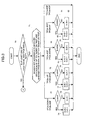
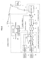
- Fig. 7 is a block diagram simply showing a conventional mobile terminal 101 in accordance with a CDMA method from an aspect of transmission power control, and here, it is assumed that data transmission is conducted from the mobile terminal 101 to a base station 102 using only one code channel.
- the data to be transmitted is supplied to the mobile terminal 101 from a signal source 104 connected to the mobile terminal 101.
- the data to be transmitted is often a voice signal, and is sometimes a high speed multi-media data that is output from a computer.
- the signal source 104 is for outputting a data stream at a bit rate of R bits/second.
- a receiver 112 connected to a reception antenna 111, a transmitter 114 connected to a transmission antenna 113, a spreading circuit 115 to which a data stream from the signal source 104 is input, a D/A (Digital/Analog) converter 116 for converting a digital signal output from the spreading circuit 115 into an analog signal, a modulator 117 for applying orthogonal modulation to a carrier wave based on an output from the D/A converter 116, a variable gain circuit 118 inserted between an output of the modulator 117 and an input of the transmitter 114.
- An oscillation circuit 119 for generating a high frequency signal that is a carrier signal is connected to the modulator 117.
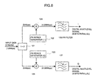
- the spreading circuit 115 After applying error correction coding and a process such as interleave and encrypt to a data stream from the signal source 104, the spreading circuit 115 spreads using a spreading code corresponding to an allocated code channel, and outputs a base band signal.
- the spreading circuit 115 is constructed as a digital signal processing circuit, and spreads the data stream from the signal source 104 to generate a signal and outputs a multilevel digital signal as a base band signal, which represents an instant value of this signal every moment.
- orthogonal modulation is conducted by means of four phases PSK (phase shift modulation) (QPSK (Quadrature Phase Shift Keying)), and accordingly, an in-phase component I and an orthogonal component Q of the base band signal are output from the spreading circuit 115 as a multilevel digital signal, respectively, and the D/A converter 116 independently converts the in-phase component I and the orthogonal component Q into analog signals, respectively, and the modulator 117 receives these in-phase component I and orthogonal component Q and conducts modulation.
- PSK phase shift modulation
- QPSK Quadrature Phase Shift Keying
- This spreading circuit 115 is for applying direct sequence (DS) system as spread spectrum system to the input data stream.
- DS direct sequence
- values in parentheses show typical examples of a data speed, a chip rate and so forth.
- a data stream of a data speed 128 kbps (bps is the number of bits per second) for example is input from the signal source, and a serial/parallel conversion circuit 121 with one input and two outputs (1 ⁇ 2) is provided for dividing this input data stream into two series of data streams with a data speed (64 kbps in this example) that is a half compared with the input data stream.
- One data stream from the serial/parallel conversion circuit 121 corresponds to the in-phase component I in the orthogonal modulation, and the other data stream corresponds to the orthogonal component Q.
- PN code generator 122 for generating a pseudorandom noise code (PN code) as a spreading code for the in-phase component I
- PN code generator 123 for generating a pseudorandom noise code (PN code) as a spreading code for the orthogonal component Q.
- the data stream and spreading code on a side of the in-phase component I are input to an adder 124, and thereby, the data stream corresponding to the in-phase component I is spreaded.
- the data stream and spreading code on a side of the orthogonal component Q are input to an adder 125, and thereby, the data stream corresponding to the orthogonal component Q is spreaded.
- the adders 124 and 125 are for calculating exclusive OR between the input data stream and the spreading code.
- a chip rate of a signal after spreading which is output from each of the adders 124 and 125 is 4.096 Mcps (cps is the number of chips per second), for example.
- the signals after spreading from the adders 124 and 125 are input to FIR (finite impulse response) filters 126 and 127 that function as a low pass filter, respectively, and thereby, a multilevel digital signal (8 bits value signal, for example) is output every moment, which represents an instant value of a base band signal of the in-phase component I and the orthogonal component Q.
- variable gain circuit 118 is constructed of an amplifier capable of varying a gain or an attenuator capable of varying an amount of attenuation.
- a gain (or an amount of attenuation) in the variable gain circuit 118 is controlled by a TPC (Total Power Control) signal from the receiver 112 1dB by 1dB, for example.
- the base station 102 After receiving such a transmission signal from the mobile terminal 101, the base station 102 applies despreading, decoding, de-interleave and error correction to this signal. It is assumed that signal power per bit necessary for fully receiving this signal in the base station 102 is E b , noise power per Hertz is N 0 , and a ratio of these is E b /N 0 .
- to fully receive the signal means that a bit error rate in a data stream output after the error correction is satisfied with a predetermined level.
- the base station 102 transmits to each mobile terminal 101 a command for controlling transmission power so as to always make a reception level of the signal to be C.
- a command for controlling transmission power so as to always make a reception level of the signal to be C.
- the base station 102 transmits a command for making transmission power of the mobile terminal 101 increase by a constant (1 dB, for example), and in case that the signal level is larger conversely, the base station 102 transmits a command for making the transmission power decrease to the mobile terminal.
- This command is called a TPC (Total Power Control) signal.
- This signal can be a command that makes the transmission power increase if its value is "1" for example, and that makes the transmission power decrease if its value is "0".
- the mobile terminal 101 receives the TPC signal at the receiver 112.
- the received TPC signal is output from the receiver 112 to the variable gain circuit 118, and the variable gain circuit 118 increases or decreases a gain by a constant (1 dB, for example) in accordance with the TPC-signal.
- the transmission signal level is adjusted to a level required by the base station 102.
- a method of controlling the transmission power of the mobile terminal in this manner is called closed loop control. This control method is generally used in an IS-95CDMA system and so forth, which is a mobile communication system in the United States.
- the present invention deals with how to control the transmission signal power of the terminal in case of conducting the multi-code transmission.
- a case can be raised, in which a voice signal and a data signal are concurrently transmitted.
- a voice signal such as a conversation
- the other is allocated to transmission of a data signal for a file exchange between computers.
- allowable error rates are different from each other between the voice signal and the data signal, and while a bit error rate of about 10 -3 is allowed for the voice signal, a bit error rate equal or less than 10 -6 is sometimes necessary for the data signal.
- a kind of the signal to be transmitted is not necessarily limited to the voice signal such as conversation and the data signal for the file exchange.
- the voice signal such as conversation and the data signal for the file exchange.
- a dynamic image data, a static image data and so forth are transmitted.
- even in the voice signal there are a case such as conversation in which relatively low voice quality is allowed, and also, a case such as music in which relatively high quality is required.
- bit error rates required for a layer of the transmission by means of the CDMA are different from each other in accordance with an upward protocol. Therefore, it is required to determine a bit error rate and so forth in accordance with a kind and characteristic of a signal (data) to be transmitted, and to precisely conduct transmission power control in accordance with the determined ratio.
- a transfer route of a data to be transmitted is changed for each code channel.
- a band width of a signal after spreading is determined by a chip rate, since, if chip rates are the same, a spreading gain is improved as a data rate becomes to be lower, it is possible to make transmission power small by the improvement. From this point also, it is required to precisely conduct transmission power control for each code channel.
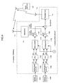
- a method can most easily be imagined, in which a plurality of circuits from the signal source 104 to variable gain circuit 118 in the circuit shown in Fig. 7 are prepared in accordance with the number of code channels to be used, and outputs from the plurality of variable gain circuits are added to each other in an analog manner by a high frequency signal adder (wave coupler), and a signal after the addition is input to the transmitter.
- Fig. 9 is a block diagram showing an arrangement of a mobile terminal for controlling transmission power by means of the method mentioned here, in which N is equal to two, that is, the number of the code channels to be used in the terminal is two.
- a circuit corresponding to a code channel A is a circuit from the signal source 104A to the variable gain circuit 118A
- a circuit corresponding to a code channel B is a circuit from the signal source 104B to the variable gain circuit 118B.
- spread codes used in the spreading circuits 115A and 115B are spread codes of the code channels A and B, respectively, and therefore, the spreading circuits 115A and 115B use spread codes different from each other.
- the oscillation circuit 119 for generating a carrier signal is provided for the modulators 117A and 117B in common.
- the outputs from both the variable gain circuits 118A and 118B are added to each other in an analog manner by the signal adder (wave coupler) 122, and an output from the signal adder 120 is input to the transmitter 114.
- a signal generated by adding the transmission signals of the code channels A and B to each other is transmitted to the base station 102.
- the base station 102 considers the code channels A and B as individual channels, respectively, and transmits a TPCA signal and a TPCB signal to the mobile terminal 121, which are TPC signals for each code channel.
- the mobile terminal 121 receives a signal from the base station 102, and controls the variable gain circuits 118A and 118B, respectively, using the received TPCA signal and TPCB signal. Thereby, closed loop power control for each code channel is conducted.
- this circuit is simply constructed by mounting a plurality of circuits from the signal source to the variable gain circuit just before the transmitter, which corresponds to the number of the multi-code, and that a circuit scale thereof is not different so much from that in the case of using individual mobile terminals for each code channel.
- high frequency circuits such as modulators and D/A converters are provided in accordance with the number of the code channels, electric power consumption becomes to be larger than that in a usual terminal.
- to provide a plurality of D/A converters directly results in the increase of electric power consumption.
- WO 97/02665 describes an automatic power control for a spread-spectrum communications system including an automatic forward power control system and an automatic reverse power control system .
- the objective of the present invention is to provide a transmission power control method and apparatus for conducting transmission power control during multi-code transmission, which can reduce a circuit scale and electric power consumption more and is capable of conducting optimum power control.
- the objective of the present invention is to provide a method of and an apparatus for adjusting transmission power in a CDMA terminal for code division multiple access communication with spread spectrum system and transmitting information with the features of the claims.
- control means can be provided for determining a level adjustment in quantity in each of the first variable gain control means and the second variable gain control means based on a control signal from the other station, for example.
- a level control calculating circuit is used, for example, which will be mentioned below in an embodiment.
- a total average level of transmission signals of the code channels can be adjusted by the second variable gain control means, and a difference of levels between the code channels can be adjusted by the first variable gain control means.
- a difference of levels between the code channels is previously set, and only a level adjustment in quantity of the second variable gain control means can be controlled in accordance with a level control signal from the other station.
- a level setting circuit can be provided for setting a level adjustment in quantity in each of the first variable gain control means based on a required level difference between the code channels.
- the level difference between the code channels can be determined using information with respect to characteristic of a transmission data in the each code channel.
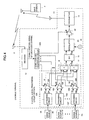
- Fig. 1 is a block diagram showing an arrangement of a mobile terminal of the first embodiment including a transmission power control apparatus of the present invention.
- the number of code channels of a multi-code is two.
- the two code channels are distinguished from each other by adding letters A and B.
- Signal sources 4A and 4B for generating data streams of code channels A and B, respectively, are connected to a mobile terminal 1.
- the mobile terminal 1 includes a receiver 12 connected to a reception antenna 11, a transmitter 14 connected to a transmission antenna 13, spreading circuits 15A and 15B for receiving data streams from the signal sources 4A and 4B, respectively, and variable gain circuits 16A and 16B disposed on output sides of the spreading circuits 15A and 15B, respectively.
- the spreading circuits 15A and 15B spread using a spreading code corresponding to an allocated code channel, and output base band signals.
- the spreading circuit 15A uses the spreading code for the code channel A
- the spreading circuit 15B uses the spreading code for the code channel B.
- the spreading circuit 15A of the code channel A outputs an in-phase component IA and an orthogonal component QA of the base band signal
- the spreading circuit 15B of the code channel B outputs an in-phase component IB and an orthogonal component QB of the base band signal.
- an internal circuit arrangement of the spreading circuits 15A and 15B is the same as the internal arrangement of the spreading circuit explained by using Fig. 8.
- variable gain circuit 16A adjusts levels of the in-phase component IA and the orthogonal component QA of the base band signal of the code channel A
- variable gain circuit 16B adjusts levels of the in-phase component IB and the orthogonal component QB of the base band signal of the code channel B.
- an adder 17 for conducting vector addition of the in-phase components IA and IB of the base band signal of each code channel and outputting a result as a combined in-phase component I and an adder 18 for conducting vector addition of the orthogonal components QA and QB and outputting a result as a combined orthogonal component Q are provided on output sides of the variable gain circuits 16A and 16B.
- the spreading circuits 15A and 15B, the variable gain circuits 16A and 16B, and the adders 17 and 18 constitute a digital signal processing circuit section 5 for conducting digital signal processing.
- the spreading circuits 15A and 15B generate signals by spreading the data streams from the signal sources 4A and 4B with spreading codes, and output multilevel digital signals representing an instant value of the generated signals every moment as base band signals.
- the variable gain circuits 16A and 16B can be constructed of coefficient multipliers (multipliers), for example, and adjust levels by multiplying the multilevel digital signals that are outputs from the spreading circuits 15A and 15B by a value corresponding to a level adjustment value, and also, output a result thereof as digital values.
- the adders 17 and 18 output as digital values the in-phase component I and the orthogonal component Q combined every moment, respectively, by digital calculation.
- a D/A (Digital/Analog) converter 19 for converting a signal of a digital value into an analog signal is provided on an output side of the adders 17 and 18.
- the D/A converter 19 converts the in-phase component I and the orthogonal component Q of the base band signals that are digital signals, respectively, and outputs an in-phase component I and an orthogonal component Q of analog signals, and the in-phase component I and the orthogonal component Q of these analog signals are input to a modulator 20.
- An oscillation circuit 21 for generating a high frequency signal that is a carrier signal is connected to the modulator 20, and the modulator 20 applies orthogonal modulation to the carrier signal by means of QPSK based on the in-phase component I and the orthogonal component Q of the base band signals from the D/A converter 19, and outputs a transmission signal.
- This transmission signal is input to the transmitter 14 through a variable gain circuit 22, and thereby, the transmission signal is transmitted to a side of the base station 2.
- the variable gain circuit 22 is for conducting a level adjustment of the transmission signal, and is constructed of an amplifier capable of varying a gain or an attenuator capable of varying an amount of attenuation.
- a level control calculating circuit 23 is provided for controlling a level adjustment value at the variable gain circuits 16A, 16B and 22.
- a TPCA signal and a TPCB signal that are TPC signals for each code channel are input to the level control calculating circuit 23 from the receiver 12, and the level control calculating circuit 23 outputs control signals A, B and C for a level adjustment to the variable gain circuits 16A, 16B and 22, respectively, based on these TPCA signal and TPCB signal.
- the mobile terminal 1 shown in Fig. 1 is constructed so as to conduct QPSK modulation after combining base band signals of both the code channels, and the variable gain circuits 16A and 16B for each code channel are provided in the digital signal processing circuit section 5 and the variable gain circuit 22 for acting upon both the code channels in common is included in the high frequency analog circuit, and the level control calculating circuit 23 is provided for properly operating the variable gain circuits 16A, 16B and 22.
- the level control calculating circuit 23 is provided for properly operating the variable gain circuits 16A, 16B and 22.
- three gain control circuits exist in all.
- the data streams of each code channel are input to the spreading circuits 15A and 15B from the signal sources 4A and 4B, and after spreading is applied, are converted into base band signals of an in-phase component and an orthogonal component.
- base band signals After a level adjustment with respect to these base band signals is conducted for every code channel by the variable gain circuits 16A and 16B, in-phase components are added to each other by the adder 17 and orthogonal components are added to each other by the adder 18, and an in-phase component I and an orthogonal component Q after combination can be obtained.
- Signals of these in-phase component I and orthogonal component Q are converted into analog signals, respectively, by the D/A converter 19, and thereafter, are input to the modulator 20. Thereby, a four phases PSK modulated high frequency signal is obtained as a transmission signal, and this transmission signal is transmitted to the base station 2 through the variable gain circuit 22 and the transmitter 14.
- the base station 2 receives a signal of each code channel from the mobile terminal 1, determines whether a reception level is a proper level for every code channel, and transmits to the mobile terminal 1 a TPCA signal and a TPCB signal that are power control signals for each code channel, in accordance with a determination result.
- the receiver 12 receives these TPCA signal and TPCB signal, and the received TPCA signal and TPCB signal are sent to the level control calculating circuit 23.
- the level control calculating circuit 23 controls the variable gain circuits 16A, 16B and 22 based on the TPCA signal and the TPCB signal.
- variable gain circuits 16A, 16B and 22 based on the TPCA signal and the TPCB signal will be explained in detail.
- the power control signals (the TPCA signal and the TPCB signal) of each code channel are for instructing one of the increase or decrease of transmission power of the code channel, and are periodically transmitted from the base station 2 (while being included in a pilot signal part of each transmission slot, for example).
- variable gain circuit 22 Since, in the variable gain circuit 22 within the high frequency analog circuit section, out of the three variable gain circuits, a wide dynamic range that exceeds 80 dB can be obtained, it is preferable to control a total average and large common variation of the two code channels by this variable gain circuit 22.
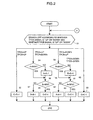
- the individual variable gain circuits 16A and 16B for the code channels are arranged inside of the digital signal processing circuit 5, respectively, and since a dynamic range of at most about 20 dB can be obtained due to the restriction of a word length of the D/A converter 19, it is preferable to limit the variable gain circuits 16A and 16B to the use for setting a level difference between the code channels. Accordingly, a control process shown in Fig. 2 is performed.
- variables A, B and C are gains in a dB unit of the variable gain circuits 16A, 16B and 22, respectively. Also, the meaning of each condition is as follows:
- a control signal C is output so as to increase a gain C of the variable gain circuit 22 by 1 dB, and the process ends.
- the control signal C is output so as to decrease the gain C of the variable gain circuit 22 by 1 dB, and the process ends.
- both the TPCA signal and TPCB signal are UP or DOWN, the transmission power control is conducted by using only the variable gain circuit 22 in the high frequency analog circuit section.
- variable gain circuits 16A and 16B are within a control range, the control is conducted by using them, and if the variable gain circuits 16A and 16B are out of the control range, the control is conducted together with the variable gain circuit 22.
- MAX maximum value
- a gain B of the variable gain circuit 16B is a minimum value (MIN), and if it is not the minimum value, after the gain B is decreased by 1 dB at STEP 57, the process ends, and if it is the minimum value, after the gain C of the variable gain circuit 22 is decreased by 1 dB at STEP 58, the process ends.
- MIN minimum value
- the gain A of the variable gain circuit 16A is a minimum value (MIN), and if it is not the minimum value, after the gain A is decreased by 1 dB at STEP 62, the process ends, and if it is the minimum value, after the gain C of the variable gain circuit 22 is decreased by 1 dB at STEP 63, the process ends.
- MIN minimum value
- the power control signals (the TPCA signal and the TPCB signal) for each code channel instruct not only to increase it by 1 dB (UP) and decrease it by 1 dB (DOWN), for example, but also not to change the transmission power (NOP).
- one of the power control signals (the TPCA signal and the TPCB signal) for every code channel is not for changing a transmission level.
- variable gain circuits 16A and 16B deal with the control, and if the variable gain circuits 16A and 16B cannot deal with the control due to a relation of the control range, the control is conducted together with the variable gain circuit 22.
- Fig. 3 is a flowchart showing a control process in case that power control signals provide three instructions such as increase of transmission power (UP), decrease of the transmission power (DOWN) and no change of the transmission power (NOP).
- UP increase of transmission power
- DOWN decrease of the transmission power
- NOP no change of the transmission power
- TPCA signal and the TPCB signal are NOP (STEP 70), and if both signals are not NOP, processing same as the above-mentioned processing shown in Fig. 2 is conducted (as illustrated as A). If at least one is NOP, the meaning of the TPCA signal and the TPCB signal is then analyzed, and the process branches off in accordance with the condition (STEP 71).
- STEP 81 it is determined whether the gain B is a maximum value, and if it is not the maximum value, after the gain B is increased by 1 dB at STEP 82, the process ends, and if it is the maximum value, at STEP 83, the gain A is decreased by 1 dB and the gain C is increased by 1 dB.
- the process of the transmission power adjustment in the mobile terminal 1 is not necessarily limited to that shown in Fig. 2 (or Fig. 3). It is possible to adjust a total average transmission level of the code channels A and B by the variable gain circuit 22 and to adjust a level difference between the code channels A and B by the variable gain circuits 16A and 16B.
- the mobile terminal of the first embodiment since the number of the D/A converter, the modulator, and the variable gain circuit disposed in the high frequency analog circuit section is one, respectively, the increase of a circuit scale and electric power consumption can be suppressed. Also, the individual variable gain circuits 16A and 16B for each code channel are provided within the digital signal processing circuit section 5, and thereby, it is possible to set a level difference between the code channels during the multi-code transmission.
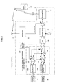
- Fig. 4 shows an arrangement of a mobile terminal 6 in case that the number of the code channels is M (M ⁇ 3).
- This mobile terminal is connected to M signal sources 4A - 4M, and M series of arrangements, each of which is from a spreading circuit to a variable gain circuit on a digital side, are provided in a digital signal processing circuit section 5.
- the digital signal processing circuit section 5 includes M spreading circuits 15A - 15M and M variable gain circuits 16A - 16M, and in-phase signals IA - IM from each of the variable gain circuits 16A - 16M are added to each other in an adder 17 and an in-phase signal I is generated, and similarly, orthogonal signals QA - QM from each of the variable gain circuits 16A - 16M are added to each other in an adder 18 and an orthogonal signal Q is generated.
- a level control calculating circuit 23A conducts control of the variable gain circuits 16A - 16M and 22.
- An arrangement on an output side of the adders 17 and 18 is the same as that in the case of the first embodiment.
- the level control calculating circuit 23A determines a level adjustment in quantity in the variable gain circuits 16A - 16M and 22 based on a TPC signal for each code channel transmitted from the base station 2. Particularly, for example, an average transmission signal level of each code channel can be adjusted by the variable gain circuit 22, and a level difference between the code channels can be adjusted by the variable gain circuits 16A - 16M.
- the number of the code channels which are used by the mobile terminal is equal to or more than three, it can be understood that if an arrangement within the digital signal processing circuit section 5 in the mobile terminal of the first embodiment is modified, the arrangement is applicable. Therefore, even though the number of the code channels that are used increases, it is possible to suppress the increase of a circuit scale and electric power consumption.
- reception levels necessary for every code channel on a side of the base station are determined by an error correcting method, a spreading ratio G and a required standard of an error rate (which is about 10 -3 for voice communication and about 10 -6 for data communication, for example) in the respective code channels.
- a difference between these reception levels is considered to be almost constant. Therefore, if considering that these code channels are transmitted from the same mobile terminal, although transmission power itself has to be controlled within a fairly wide range, it is considered that a difference of required transmission power between the code channels is specifically determined in accordance with a difference of transmission methods and so forth.
- a mobile terminal 7 shown in Fig. 5 is constructed so that a level setting circuit 24 is provided for discriminating the kind of signals of the signal sources 4A and 4B, calculating a level difference between the code channels A and B and conducting the setting of the variable gain circuits 16A and 16B, instead of providing the level control calculating circuit 23 in the mobile terminal 1 shown in Fig. 1.
- variable gain circuit 22 If a relative level difference is set in the variable gain circuits 16A and 16B by the level setting circuit 24 that is uniquely included in the mobile terminal 7, power control can be realized by controlling the variable gain circuit 22 using a power control signal (one of a TPCA signal and a TPCB signal, simply referred to as a TPC signal, hereinafter) from the base station 2.
- a power control signal one of a TPCA signal and a TPCB signal, simply referred to as a TPC signal, hereinafter
- a relative level between the code channels is previously calculated based on a bit rate, an error correcting method, a spreading ratio, a required error rate and so forth, and the calculated level is stored in a ROM (Read Only Memory) and is read from the level setting circuit 24, it is not necessary to conduct a calculation, and it is possible to simplify a circuit more and to reduce electric power consumption.
- ROM Read Only Memory
- variable gain circuits in all which are consisted of M variable gain circuits, and one variable gain circuit on an output side of a modulator, are provided within the digital signal processing circuit 5.
- M since the number of the code channels, which is an object to be controlled, is M, originally, it should be appropriate to provide M variable gain circuits in all. If considering that an enough dynamic range cannot be provided in the variable gain circuits disposed within the digital signal processing circuit section, the variable gain circuit within the high frequency circuit section is essential. Accordingly, an arrangement can be considered, in which the variable gain circuit for specific one code channel is omitted in the digital signal processing circuit section.
- This mobile terminal 8 is constructed so that the variable gain circuit 16A on a side of the code channel A in the mobile terminal 1 shown in Fig. 1 is removed, and base band signals of an in-phase component and an orthogonal component from the spreading circuit 15A are directly input to the adders 17 and 18, respectively.
- the level control calculating circuit 23 controls the variable gain circuits 16B and 22 based on a TPCA signal and a TPCB signal.
- a level adjustment in quantity at each variable gain circuit is specifically determined.
- the level can be adjusted by an amount corresponding to the adjustment in quantity by means of the variable gain circuit 22, and the level can be adjusted by an amount corresponding to that in which a sign of the adjustment in quantity is reversed, by means of the variable gain circuit 16B of the code channel B.
- the level can be adjusted based on the adjustment in quantity by the variable gain circuit 16B.
- the levels can be adjusted by an adjustment in quantity, which is generated by combining the adjustment in quantity in the case of adjusting only the code channel A and the adjustment in quantity in the case of adjusting only the code channel B, by means of each of the variable gain circuits 16B and 22.
- the transmission power control at the mobile terminal in the mobile communication system was explained.
- the present invention is applicable to a CDMA system other than the mobile communication system, and for example, to a system in which a terminal is assumed not to move.
- a wireless local loop system and so forth which is used, instead of a wire tele-communication network, in constructing a tele-communication network in an area having small population density and in developing countries.
- the kind of the spread spectrum system it is not limited to the Direct Sequence (DS), and frequency hopping (FH) and chirp spreading, for example, can be used.
- the modulation method in the modulator it is not limited to orthogonal modulation by means of QPSK, and a modulation method such as ⁇ /4 shift QPSK, DPSK (differential phase shift keying), and BPSK (binary phase shift keying) can be adopted.
- the present invention effects an advantage that even in case of using a plurality of code channels and conducting the transmission power control for every code channel, since only one variable gain circuit for adjusting a level difference between the code channels is needed, which is to be disposed in a high frequency circuit part, it is possible to suppress the increase of a circuit scale and electric power consumption.
Landscapes
- Engineering & Computer Science (AREA)
- Computer Networks & Wireless Communication (AREA)
- Signal Processing (AREA)
- Mobile Radio Communication Systems (AREA)
- Transmitters (AREA)
Claims (18)
- Verfahren zum Einstellen der Sendeleistung in einem CDMA-Endgerät (1, 6, 7, 8) für die Codemultiplex-Vielfachzugriff-Kommunikation mit einem Spreizspektrumssystem und zum Übertragen von Informationen unter Verwendung mehrerer Codekanäle mit den folgenden Schritten:Erzeugen von Basisbandsignalen durch Spreizen von Daten jedes Codekanals,Einstellen der Pegel der Basisbandsignale jedes Codekanals,Addieren der eingestellten Basisbandsignale der mehreren Codekanäle,Modulieren auf der Grundlage des Signals nach der Addition zum Erzeugen eines Hochfrequenzsignals,Einstellen des Pegels des Hochfrequenzsignals undSenden des eingestellten Hochfrequenzsignals zu einer anderen Station (2), die mit dem Endgerät kommuniziert.
- Verfahren nach Anspruch 1, wobei die Einstellung der Pegel der Basisbandsignale und die Einstellung des Pegels des Hochfrequenzsignals auf der Grundlage eines Steuersignals von der anderen Station (2) festgelegt werden.
- Verfahren nach Anspruch 1 oder 2, wobei die Pegel der Basisbandsignale nicht geändert werden und nur ein Pegel des Hochfrequenzsignals geändert wird, wenn das Steuersignal für das Erhöhen oder Verringern der Pegel um einen konstanten Betrag, der jedem der Codekanäle gemeinsam ist, vorgesehen ist.
- Verfahren nach Anspruch 1, 2 oder 3, wobei der Schritt des Einstellens eines Pegels des Hochfrequenzsignals einen Schritt des Einstellens eines durchschnittlichen Gesamtpegels von Sendesignalen der Codekanäle aufweist und der Schritt des Einstellens der Pegel der Basisbandsignale einen Schritt des Einstellens einer Pegeldifferenz zwischen den Codekanälen aufweist.
- Verfahren nach Anspruch 1 oder 2, welches weiter den folgenden Schritt aufweist:Bestimmen einer Pegeldifferenz zwischen den Codekanälen entsprechend Übertragungseigenschaften von Daten der Codekanäle, wobei der Pegel für jeden Codekanal entsprechend der bestimmten Pegeldifferenz eingestellt wird.
- Verfahren zum Einstellen der Sendeleistung in einem CDMA-Endgerät nach Anspruch 1, wobei die Einstellung der Pegel der Basisbandsignale für einen spezifischen Codekanal nicht ausgeführt wird.
- Verfahren nach einem der Ansprüche 1 bis 6, wobei das CDMA-Endgerät eine Mobilstation in einem Mobilkommunikationssystem ist und die andere Station eine Basisstation in dem Mobilkommunikationssystem ist.
- Verfahren nach einem der Ansprüche 1 bis 7, wobei das Spreizspektrumssystem ein Direktsequenzsystem ist.
- Vorrichtung zum Einstellen der Sendeleistung in einem CDMA-Endgerät (1, 6, 7, 8) für die Codemultiplex-Vielfachzugriff-Kommunikation mit einem Spreizspektrumssystem und zum Übertragen von Informationen unter Verwendung mehrerer Codekanäle, welche aufweist:mehrere Spreizeinrichtungen (15A, 15B, 15M), die für jeden Codekanal angeordnet sind, wobei die Spreizeinrichtungen dem Spreizen von Daten dienen,mehrere erste Steuereinrichtungen (16A, 16B, 16M) mit veränderlicher Verstärkung, die für jeden der Codekanäle angeordnet sind, wobei die erste Steuereinrichtung mit veränderlicher Verstärkung dem Einstellen der Pegel der Ausgangssignale von den Spreizeinrichtungen (15A, 15B, 15M) dient,einen Addierer (17, 18) zum Addieren der Ausgaben von jeder der ersten Steuereinrichtungen (16A, 16B, 16M) mit veränderlicher Verstärkung,einen Modulator (20) zum Modulieren der Ausgabe von dem Addierer (17, 18) und zum Ausgeben eines Hochfrequenzsignals undeine zweite Steuereinrichtung (22) mit veränderlicher Verstärkung zum Einstellen des Pegels des Hochfrequenzsignals.
- Vorrichtung nach Anspruch 9, welche weiter aufweist:einen Sender (14) zum Senden eines Ausgangssignals von der zweiten Steuereinrichtung (22) mit veränderlicher Verstärkung zu einer anderen Station (2), die mit dem Endgerät kommuniziert.
- Vorrichtung nach Anspruch 10, weiter aufweisend:eine Steuereinrichtung (23) zum Bestimmen einer Pegeleinstellung in jeder der ersten Steuereinrichtungen (16A, 16B, 16M) mit veränderlicher Verstärkung und der zweiten Steuereinrichtung (22) mit veränderlicher Verstärkung auf der Grundlage eines Steuersignals von der anderen Station (2).
- Vorrichtung nach Anspruch 10 oder 11, wobei das CDMA-Endgerät (1, 6, 7, 8) eine Mobilstation in einem Mobilkommunikationssystem ist und die andere Station (2) eine Basisstation in dem Mobilkommunikationssystem ist.
- Vorrichtung nach Anspruch 9, 10, 11 oder 12, wobei das Spreizspektrumssystem ein Direktsequenzsystem ist.
- Vorrichtung nach einem der Ansprüche 9 bis 13, wobei der durchschnittliche Gesamtpegel von Sendesignalen der Codekanäle durch die zweite Steuereinrichtung (22) mit veränderlicher Verstärkung eingestellt wird und die Pegeldifferenz zwischen den Codekanälen von der ersten Steuereinrichtung (16A, 16B, 16M) mit veränderlicher Verstärkung eingestellt wird.
- Vorrichtung nach einem der Ansprüche 10 bis 14, welche weiter aufweist:eine Pegelfestlegungsschaltung (24) zum Festlegen einer Pegeleinstellung in jeder der ersten Steuereinrichtungen (16A, 16B, 16M) mit veränderlicher Verstärkung auf der Grundlage einer erforderlichen Pegeldifferenz zwischen den Codekanälen undeine Steuereinrichtung (11, 12) zum Bestimmen einer Pegeleinstellung in der zweiten Steuereinrichtung (22) mit veränderlicher Verstärkung auf der Grundlage eines Steuersignals von der anderen Station (2).
- Vorrichtung nach einem der Ansprüche 9 bis 15, wobei die erforderliche Pegeldifferenz unter Verwendung von Informationen in Bezug auf Eigenschaften von Übertragungsdaten in jedem Codekanal bestimmt wird.
- Vorrichtung zum Einstellen der Sendeleistung in einem CDMA-Endgerät nach Anspruch 9, wobei die ersten Steuereinrichtungen (16A, 16B, 16M) mit veränderlicher Verstärkung nicht in einem spezifischen Codekanal angeordnet sind.
- Vorrichtung nach einem der Ansprüche 9 bis 17, wobei jede der Spreizschaltungen (15A, 15B, 15M) und jede der ersten Steuereinrichtungen (16A, 16B, 16M) mit veränderlicher Verstärkung in einem Digitalsignalverarbeitungs-Schaltungsabschnitt angeordnet sind und die zweite Steuereinrichtung (22) mit veränderlicher Verstärkung als eine Hochfrequenz-Analogschaltung aufgebaut ist.
Priority Applications (5)
| Application Number | Priority Date | Filing Date | Title |
|---|---|---|---|
| EP10012490.8A EP2296416A3 (de) | 1998-03-18 | 1999-03-16 | Verfahren und Vorrichtung zur Regelung der Sendeleistung in einem CDMA Gerät |
| EP10012487.4A EP2296413A3 (de) | 1998-03-18 | 1999-03-16 | Verfahren und Vorrichtung zur Regelung der Sendeleistung in einem CDMA Gerät |
| EP10012489.0A EP2296415A3 (de) | 1998-03-18 | 1999-03-16 | Verfahren und Vorrichtung zur Regelung der Sendeleistung in einem CDMA Gerät |
| EP10012488.2A EP2296414A3 (de) | 1998-03-18 | 1999-03-16 | Verfahren und Vorrichtung zur Regelung der Sendeleistung in einem CDMA Gerät |
| EP05023249.5A EP1630971B1 (de) | 1998-03-18 | 1999-03-16 | Verfahren und Vorrichtung zur Regelung der Sendeleistung in einem CDMA Gerät |
Applications Claiming Priority (2)
| Application Number | Priority Date | Filing Date | Title |
|---|---|---|---|
| JP6858998 | 1998-03-18 | ||
| JP6858998A JP3109589B2 (ja) | 1998-03-18 | 1998-03-18 | Cdma端末の送信パワー調整方法及び装置 |
Related Child Applications (5)
| Application Number | Title | Priority Date | Filing Date |
|---|---|---|---|
| EP10012488.2A Division EP2296414A3 (de) | 1998-03-18 | 1999-03-16 | Verfahren und Vorrichtung zur Regelung der Sendeleistung in einem CDMA Gerät |
| EP10012487.4A Division EP2296413A3 (de) | 1998-03-18 | 1999-03-16 | Verfahren und Vorrichtung zur Regelung der Sendeleistung in einem CDMA Gerät |
| EP05023249.5A Division EP1630971B1 (de) | 1998-03-18 | 1999-03-16 | Verfahren und Vorrichtung zur Regelung der Sendeleistung in einem CDMA Gerät |
| EP10012489.0A Division EP2296415A3 (de) | 1998-03-18 | 1999-03-16 | Verfahren und Vorrichtung zur Regelung der Sendeleistung in einem CDMA Gerät |
| EP10012490.8A Division EP2296416A3 (de) | 1998-03-18 | 1999-03-16 | Verfahren und Vorrichtung zur Regelung der Sendeleistung in einem CDMA Gerät |
Publications (3)
| Publication Number | Publication Date |
|---|---|
| EP0944182A2 EP0944182A2 (de) | 1999-09-22 |
| EP0944182A3 EP0944182A3 (de) | 2003-02-12 |
| EP0944182B1 true EP0944182B1 (de) | 2005-10-26 |
Family
ID=13378145
Family Applications (6)
| Application Number | Title | Priority Date | Filing Date |
|---|---|---|---|
| EP10012490.8A Withdrawn EP2296416A3 (de) | 1998-03-18 | 1999-03-16 | Verfahren und Vorrichtung zur Regelung der Sendeleistung in einem CDMA Gerät |
| EP10012488.2A Withdrawn EP2296414A3 (de) | 1998-03-18 | 1999-03-16 | Verfahren und Vorrichtung zur Regelung der Sendeleistung in einem CDMA Gerät |
| EP10012489.0A Withdrawn EP2296415A3 (de) | 1998-03-18 | 1999-03-16 | Verfahren und Vorrichtung zur Regelung der Sendeleistung in einem CDMA Gerät |
| EP05023249.5A Expired - Lifetime EP1630971B1 (de) | 1998-03-18 | 1999-03-16 | Verfahren und Vorrichtung zur Regelung der Sendeleistung in einem CDMA Gerät |
| EP19990105392 Expired - Lifetime EP0944182B1 (de) | 1998-03-18 | 1999-03-16 | Verfahren und Vorrichtung zur Regelung der Sendeleistung in einem CDMA-Endgerät |
| EP10012487.4A Withdrawn EP2296413A3 (de) | 1998-03-18 | 1999-03-16 | Verfahren und Vorrichtung zur Regelung der Sendeleistung in einem CDMA Gerät |
Family Applications Before (4)
| Application Number | Title | Priority Date | Filing Date |
|---|---|---|---|
| EP10012490.8A Withdrawn EP2296416A3 (de) | 1998-03-18 | 1999-03-16 | Verfahren und Vorrichtung zur Regelung der Sendeleistung in einem CDMA Gerät |
| EP10012488.2A Withdrawn EP2296414A3 (de) | 1998-03-18 | 1999-03-16 | Verfahren und Vorrichtung zur Regelung der Sendeleistung in einem CDMA Gerät |
| EP10012489.0A Withdrawn EP2296415A3 (de) | 1998-03-18 | 1999-03-16 | Verfahren und Vorrichtung zur Regelung der Sendeleistung in einem CDMA Gerät |
| EP05023249.5A Expired - Lifetime EP1630971B1 (de) | 1998-03-18 | 1999-03-16 | Verfahren und Vorrichtung zur Regelung der Sendeleistung in einem CDMA Gerät |
Family Applications After (1)
| Application Number | Title | Priority Date | Filing Date |
|---|---|---|---|
| EP10012487.4A Withdrawn EP2296413A3 (de) | 1998-03-18 | 1999-03-16 | Verfahren und Vorrichtung zur Regelung der Sendeleistung in einem CDMA Gerät |
Country Status (8)
| Country | Link |
|---|---|
| US (2) | US6553018B1 (de) |
| EP (6) | EP2296416A3 (de) |
| JP (1) | JP3109589B2 (de) |
| KR (1) | KR100333427B1 (de) |
| CN (1) | CN1114295C (de) |
| DE (1) | DE69927863T2 (de) |
| SG (1) | SG75930A1 (de) |
| TW (1) | TW448645B (de) |
Families Citing this family (39)
| Publication number | Priority date | Publication date | Assignee | Title |
|---|---|---|---|---|
| JP3317259B2 (ja) | 1998-12-17 | 2002-08-26 | 日本電気株式会社 | ベースバンド信号多重回路とその送信レベル制御方法 |
| JP2000349640A (ja) | 1999-06-02 | 2000-12-15 | Nec Corp | 符号分割多重化送信装置 |
| GB9922239D0 (en) * | 1999-09-20 | 1999-11-17 | Nokia Mobile Phones Ltd | A multiple access technique for mobile radio systems |
| US6693956B1 (en) * | 1999-10-08 | 2004-02-17 | Hitachi Denshi Kabushiki Kaisha | Power amplifier having negative feedback circuit for transmitter |
| US6717981B1 (en) * | 1999-12-14 | 2004-04-06 | Koninklijke Philips Electronics N.V. | Transmitter image suppression in TDD transceivers |
| JP3618071B2 (ja) | 1999-12-28 | 2005-02-09 | 株式会社エヌ・ティ・ティ・ドコモ | 移動通信制御方法及びそのシステム及びそれに用いられる基地局及び移動局 |
| KR20010087669A (ko) * | 2000-03-08 | 2001-09-21 | 서평원 | 통신 시스템의 기지국 송신 장치 |
| JP2001285193A (ja) * | 2000-03-29 | 2001-10-12 | Oki Electric Ind Co Ltd | 送信電力制御方式 |
| CN1161916C (zh) | 2000-03-30 | 2004-08-11 | 三菱电机株式会社 | 多路复用通信系统的信号处理装置及其信号处理方法 |
| JP2001285089A (ja) * | 2000-03-31 | 2001-10-12 | Matsushita Electric Ind Co Ltd | 無線通信装置及び送信電力制御方法 |
| EP1317081A4 (de) * | 2000-07-14 | 2009-12-02 | Sanyo Electric Co | Drahtloses informationsendgerät, drahtloses kommunikationssystem, kommunikationsverfahren und programm |
| US6999500B2 (en) * | 2000-11-03 | 2006-02-14 | Qualcomm Inc. | System for direct sequence spreading |
| JP2002176390A (ja) | 2000-12-05 | 2002-06-21 | Nec Corp | 送信電力制御装置、方法及びコンピュータ読み取り可能な記録媒体 |
| JP3956085B2 (ja) | 2000-12-20 | 2007-08-08 | 日本電気株式会社 | 送信回路 |
| US7120134B2 (en) | 2001-02-15 | 2006-10-10 | Qualcomm, Incorporated | Reverse link channel architecture for a wireless communication system |
| US7570709B2 (en) * | 2001-03-08 | 2009-08-04 | Siemens Aktiengesellschaft | Automatic transmit power control loop with modulation averaging |
| JP4763908B2 (ja) * | 2001-03-28 | 2011-08-31 | 富士通東芝モバイルコミュニケーションズ株式会社 | 無線通信端末及びその制御回路 |
| JP3666430B2 (ja) | 2001-09-04 | 2005-06-29 | ソニー株式会社 | 情報送信装置及び情報送信方法、並びに情報受信装置及び情報受信方法 |
| US6717931B2 (en) * | 2002-01-02 | 2004-04-06 | Nokia Corporation | Adaptive spreading factor based on power control |
| US6650691B2 (en) * | 2002-02-12 | 2003-11-18 | Motorola, Inc. | Power control in spread spectrum communications systems |
| JP4014893B2 (ja) * | 2002-03-01 | 2007-11-28 | 株式会社エヌ・ティ・ティ・ドコモ | マルチホップ接続用の無線通信システム、無線通信方法、これに用いる無線局 |
| KR100765873B1 (ko) * | 2002-07-19 | 2007-10-11 | 인터디지탈 테크날러지 코포레이션 | 수신 다이버시티를 갖는 블록 전송을 위한 그룹형 직렬간섭 제거 |
| US7068703B2 (en) * | 2003-02-18 | 2006-06-27 | Qualcomm, Incorporated | Frequency hop sequences for multi-band communication systems |
| WO2004100396A1 (en) * | 2003-05-09 | 2004-11-18 | Philips Intellectual Property & Standards Gmbh | Method and arrangement for setting the transmission power of a mobile communication device |
| US7031678B2 (en) * | 2003-07-15 | 2006-04-18 | Qualcomm Inc. | Wireless speech and data transmission |
| US7899419B2 (en) * | 2004-01-16 | 2011-03-01 | Research In Motion Limited | Method and apparatus for compensating code channel power in a transmitter |
| US7333784B2 (en) * | 2004-01-16 | 2008-02-19 | Research In Motion Limited | Method and apparatus for compensating code channel power in a transmitter |
| US7640621B2 (en) * | 2004-04-26 | 2010-01-05 | Panasonic Corporation Of North America | Thermal protection system for electrical appliance |
| US7664520B2 (en) | 2004-06-24 | 2010-02-16 | Nokia Corporation | Low current direct conversion transmitter architecture |
| JP2006186873A (ja) * | 2004-12-28 | 2006-07-13 | Matsushita Electric Ind Co Ltd | 無線装置および送信出力変更方法 |
| KR101315478B1 (ko) | 2005-12-08 | 2013-10-07 | 한국전자통신연구원 | 단말기 및 그 송신 전력 제어 방법 |
| WO2007067004A2 (en) * | 2005-12-08 | 2007-06-14 | Samsung Electronics Co., Ltd. | Terminal and method for controlling transmission power |
| US8668146B1 (en) | 2006-05-25 | 2014-03-11 | Sean I. Mcghie | Rewards program with payment artifact permitting conversion/transfer of non-negotiable credits to entity independent funds |
| JP4494445B2 (ja) * | 2007-09-03 | 2010-06-30 | 株式会社エヌ・ティ・ティ・ドコモ | 送信電力制御方法及び装置 |
| US7702290B1 (en) * | 2009-04-08 | 2010-04-20 | On-Ramp Wirless, Inc. | Dynamic energy control |
| JP5603647B2 (ja) * | 2009-05-13 | 2014-10-08 | キヤノン株式会社 | 給電装置、給電装置の制御方法及び給電通信システム |
| JP5606436B2 (ja) | 2009-06-08 | 2014-10-15 | シャープ株式会社 | 送信電力制御方法および送信装置 |
| US8678786B2 (en) | 2010-10-21 | 2014-03-25 | Honeywell International Inc. | Scroll compressor with partial unloader for start-up |
| US9325372B2 (en) * | 2013-08-12 | 2016-04-26 | Broadcom Corporation | Upstream power amplifier |
Family Cites Families (15)
| Publication number | Priority date | Publication date | Assignee | Title |
|---|---|---|---|---|
| US5103459B1 (en) | 1990-06-25 | 1999-07-06 | Qualcomm Inc | System and method for generating signal waveforms in a cdma cellular telephone system |
| US5870393A (en) * | 1995-01-20 | 1999-02-09 | Hitachi, Ltd. | Spread spectrum communication system and transmission power control method therefor |
| JP3457357B2 (ja) * | 1993-07-23 | 2003-10-14 | 株式会社日立製作所 | スペクトル拡散通信システム、送信電力制御方法、移動端末装置及び基地局 |
| US6049535A (en) * | 1996-06-27 | 2000-04-11 | Interdigital Technology Corporation | Code division multiple access (CDMA) communication system |
| ZA965340B (en) * | 1995-06-30 | 1997-01-27 | Interdigital Tech Corp | Code division multiple access (cdma) communication system |
| JPH0923207A (ja) | 1995-07-07 | 1997-01-21 | Toshiba Corp | 情報多重化方式 |
| US5745480A (en) * | 1996-04-03 | 1998-04-28 | Adicom Wireless, Inc. | Multi-rate wireless communications system |
| JPH09298489A (ja) | 1996-05-08 | 1997-11-18 | Matsushita Electric Ind Co Ltd | Cdma方式移動通信装置 |
| US5930230A (en) | 1996-05-28 | 1999-07-27 | Qualcomm Incorporated | High data rate CDMA wireless communication system |
| KR100289568B1 (ko) * | 1996-07-29 | 2001-05-02 | 다치카와 게이지 | 사이트 다이버시티를 이용한 이동 통신 시스템에 있어서의 다운링크 송신 전력 제어 방법 및 장치 |
| US5862460A (en) * | 1996-09-13 | 1999-01-19 | Motorola, Inc. | Power control circuit for a radio frequency transmitter |
| US5933781A (en) * | 1997-01-31 | 1999-08-03 | Qualcomm Incorporated | Pilot based, reversed channel power control |
| JP3628145B2 (ja) * | 1997-05-21 | 2005-03-09 | 松下電器産業株式会社 | 送信電力制御装置及び送信電力制御方法 |
| JP2856250B2 (ja) * | 1997-06-27 | 1999-02-10 | 日本電気株式会社 | コード多重通信方式における増幅部利得補償装置 |
| US6072784A (en) * | 1997-07-25 | 2000-06-06 | At&T Corp. | CDMA mobile station wireless transmission power management with adaptive scheduling priorities based on battery power level |
-
1998
- 1998-03-18 JP JP6858998A patent/JP3109589B2/ja not_active Expired - Lifetime
-
1999
- 1999-03-16 EP EP10012490.8A patent/EP2296416A3/de not_active Withdrawn
- 1999-03-16 EP EP10012488.2A patent/EP2296414A3/de not_active Withdrawn
- 1999-03-16 DE DE1999627863 patent/DE69927863T2/de not_active Expired - Lifetime
- 1999-03-16 EP EP10012489.0A patent/EP2296415A3/de not_active Withdrawn
- 1999-03-16 EP EP05023249.5A patent/EP1630971B1/de not_active Expired - Lifetime
- 1999-03-16 EP EP19990105392 patent/EP0944182B1/de not_active Expired - Lifetime
- 1999-03-16 EP EP10012487.4A patent/EP2296413A3/de not_active Withdrawn
- 1999-03-17 SG SG1999001137A patent/SG75930A1/en unknown
- 1999-03-17 TW TW88104119A patent/TW448645B/zh not_active IP Right Cessation
- 1999-03-18 CN CN99103373A patent/CN1114295C/zh not_active Expired - Lifetime
- 1999-03-18 US US09/271,103 patent/US6553018B1/en not_active Ceased
- 1999-03-18 KR KR1019990009160A patent/KR100333427B1/ko not_active Expired - Lifetime
-
2005
- 2005-04-22 US US11/113,336 patent/USRE40553E1/en not_active Expired - Lifetime
Also Published As
| Publication number | Publication date |
|---|---|
| JP3109589B2 (ja) | 2000-11-20 |
| CN1237049A (zh) | 1999-12-01 |
| EP1630971A2 (de) | 2006-03-01 |
| EP1630971A3 (de) | 2010-10-06 |
| EP2296413A2 (de) | 2011-03-16 |
| US6553018B1 (en) | 2003-04-22 |
| KR19990078013A (ko) | 1999-10-25 |
| EP1630971B1 (de) | 2015-10-07 |
| DE69927863T2 (de) | 2006-07-27 |
| EP2296413A3 (de) | 2015-12-02 |
| SG75930A1 (en) | 2000-10-24 |
| KR100333427B1 (ko) | 2002-04-18 |
| EP2296416A3 (de) | 2015-12-16 |
| EP2296414A2 (de) | 2011-03-16 |
| EP0944182A2 (de) | 1999-09-22 |
| EP2296414A3 (de) | 2015-12-09 |
| DE69927863D1 (de) | 2005-12-01 |
| EP2296416A2 (de) | 2011-03-16 |
| CN1114295C (zh) | 2003-07-09 |
| EP2296415A3 (de) | 2015-12-16 |
| EP0944182A3 (de) | 2003-02-12 |
| USRE40553E1 (en) | 2008-10-28 |
| JPH11266168A (ja) | 1999-09-28 |
| EP2296415A2 (de) | 2011-03-16 |
| TW448645B (en) | 2001-08-01 |
Similar Documents
| Publication | Publication Date | Title |
|---|---|---|
| EP0944182B1 (de) | Verfahren und Vorrichtung zur Regelung der Sendeleistung in einem CDMA-Endgerät | |
| US6031865A (en) | Rapidly decorrelating spreading sequences for DS-CDMA transceivers | |
| KR100633854B1 (ko) | 부호분할을 사용하는 두 병렬채널의 전송방법 및 그 방법을 구현하는 장치 | |
| US6396868B1 (en) | Spread spectrum signal generating device and method in transmitter of mobile communications system | |
| EP1048138B1 (de) | Gerät und verfahren zur generierung eines spreizkodes und kanalsignalspreizung unter verwendung eines spreizkodes in einem cdma-übertragungssystem | |
| EP0682423A2 (de) | Kode-Mehrfachzugriffsverfahren, das dem Benutzer variablen Datenratenzugriff liefert | |
| WO1997037457A1 (en) | Multi-rate wireless communications system | |
| WO1997037457A9 (en) | Multi-rate wireless communications system | |
| USRE37420E1 (en) | Automobile on-board and/or portable telephone system | |
| KR100429534B1 (ko) | 이동통신시스템의 핸드오프시 역방향 전력제어채널의전송제어를 위한 방법 및 장치 | |
| EP1053648A1 (de) | Gerät und verfahren zur kanalspreizung in einem cdma kommunikationssytem | |
| JP3144780B2 (ja) | スペクトル拡散変調可変多重伝送装置 | |
| EP0903871B1 (de) | Spreizspektrumsignalerzeugungseinrichtung und -verfahren | |
| JP3473693B2 (ja) | Cdma端末の送信パワー調整方法及び装置 | |
| JP3421210B2 (ja) | Cdma移動通信システムにおける信号伝送方法及び信号送信装置 | |
| USRE39954E1 (en) | Automobile on-board and/or portable telephone system | |
| JP2793985B2 (ja) | 可変容量スペクトル拡散伝送装置 | |
| KR20050118064A (ko) | 비동기 이동통신 시스템에서 향상된 상향링크 채널을 통해데이터 전송 시 최대전력대 평균전력비 감소를 위한직교가변확산코드 코드와 직교위상 채널의 할당 방법 및장치 | |
| KR20050118082A (ko) | 비동기 이동통신 시스템에서 향상된 상향링크 채널을 통해데이터 전송 시 최대전력대 평균전력비 감소를 위한직교가변확산코드 코드와 직교위상 채널의 할당 방법 및장치 | |
| HK1099139B (en) | Reduced peak-to-average amplitude multichannel |
Legal Events
| Date | Code | Title | Description |
|---|---|---|---|
| PUAI | Public reference made under article 153(3) epc to a published international application that has entered the european phase |
Free format text: ORIGINAL CODE: 0009012 |
|
| AK | Designated contracting states |
Kind code of ref document: A2 Designated state(s): AT BE CH CY DE DK ES FI FR GB GR IE IT LI LU MC NL PT SE |
|
| AX | Request for extension of the european patent |
Free format text: AL;LT;LV;MK;RO;SI |
|
| PUAL | Search report despatched |
Free format text: ORIGINAL CODE: 0009013 |
|
| AK | Designated contracting states |
Designated state(s): AT BE CH CY DE DK ES FI FR GB GR IE IT LI LU MC NL PT SE |
|
| AX | Request for extension of the european patent |
Extension state: AL LT LV MK RO SI |
|
| 17P | Request for examination filed |
Effective date: 20030107 |
|
| AKX | Designation fees paid |
Designated state(s): DE GB IT SE |
|
| 17Q | First examination report despatched |
Effective date: 20040726 |
|
| GRAP | Despatch of communication of intention to grant a patent |
Free format text: ORIGINAL CODE: EPIDOSNIGR1 |
|
| GRAS | Grant fee paid |
Free format text: ORIGINAL CODE: EPIDOSNIGR3 |
|
| GRAA | (expected) grant |
Free format text: ORIGINAL CODE: 0009210 |
|
| AK | Designated contracting states |
Kind code of ref document: B1 Designated state(s): DE GB IT SE |
|
| REG | Reference to a national code |
Ref country code: GB Ref legal event code: FG4D |
|
| REF | Corresponds to: |
Ref document number: 69927863 Country of ref document: DE Date of ref document: 20051201 Kind code of ref document: P |
|
| REG | Reference to a national code |
Ref country code: SE Ref legal event code: TRGR |
|
| PLBE | No opposition filed within time limit |
Free format text: ORIGINAL CODE: 0009261 |
|
| STAA | Information on the status of an ep patent application or granted ep patent |
Free format text: STATUS: NO OPPOSITION FILED WITHIN TIME LIMIT |
|
| 26N | No opposition filed |
Effective date: 20060727 |
|
| PGFP | Annual fee paid to national office [announced via postgrant information from national office to epo] |
Ref country code: GB Payment date: 20180314 Year of fee payment: 20 Ref country code: DE Payment date: 20180306 Year of fee payment: 20 |
|
| PGFP | Annual fee paid to national office [announced via postgrant information from national office to epo] |
Ref country code: IT Payment date: 20180321 Year of fee payment: 20 Ref country code: SE Payment date: 20180313 Year of fee payment: 20 |
|
| REG | Reference to a national code |
Ref country code: DE Ref legal event code: R071 Ref document number: 69927863 Country of ref document: DE |
|
| REG | Reference to a national code |
Ref country code: GB Ref legal event code: PE20 Expiry date: 20190315 |
|
| PG25 | Lapsed in a contracting state [announced via postgrant information from national office to epo] |
Ref country code: GB Free format text: LAPSE BECAUSE OF EXPIRATION OF PROTECTION Effective date: 20190315 |