EP0944286A2 - Vorrichtung für Asynchronen transfer mode - Google Patents
Vorrichtung für Asynchronen transfer mode Download PDFInfo
- Publication number
- EP0944286A2 EP0944286A2 EP99104037A EP99104037A EP0944286A2 EP 0944286 A2 EP0944286 A2 EP 0944286A2 EP 99104037 A EP99104037 A EP 99104037A EP 99104037 A EP99104037 A EP 99104037A EP 0944286 A2 EP0944286 A2 EP 0944286A2
- Authority
- EP
- European Patent Office
- Prior art keywords
- atm
- cell
- routing information
- devices
- phy layer
- Prior art date
- Legal status (The legal status is an assumption and is not a legal conclusion. Google has not performed a legal analysis and makes no representation as to the accuracy of the status listed.)
- Granted
Links
Images









Classifications
-
- H—ELECTRICITY
- H04—ELECTRIC COMMUNICATION TECHNIQUE
- H04L—TRANSMISSION OF DIGITAL INFORMATION, e.g. TELEGRAPHIC COMMUNICATION
- H04L49/00—Packet switching elements
- H04L49/40—Constructional details, e.g. power supply, mechanical construction or backplane
- H04L49/405—Physical details, e.g. power supply, mechanical construction or backplane of ATM switches
-
- H—ELECTRICITY
- H04—ELECTRIC COMMUNICATION TECHNIQUE
- H04Q—SELECTING
- H04Q11/00—Selecting arrangements for multiplex systems
- H04Q11/04—Selecting arrangements for multiplex systems for time-division multiplexing
- H04Q11/0428—Integrated services digital network, i.e. systems for transmission of different types of digitised signals, e.g. speech, data, telecentral, television signals
- H04Q11/0478—Provisions for broadband connections
-
- H—ELECTRICITY
- H04—ELECTRIC COMMUNICATION TECHNIQUE
- H04L—TRANSMISSION OF DIGITAL INFORMATION, e.g. TELEGRAPHIC COMMUNICATION
- H04L12/00—Data switching networks
- H04L12/54—Store-and-forward switching systems
- H04L12/56—Packet switching systems
- H04L12/5601—Transfer mode dependent, e.g. ATM
- H04L2012/5603—Access techniques
- H04L2012/5604—Medium of transmission, e.g. fibre, cable, radio
- H04L2012/5605—Fibre
-
- H—ELECTRICITY
- H04—ELECTRIC COMMUNICATION TECHNIQUE
- H04L—TRANSMISSION OF DIGITAL INFORMATION, e.g. TELEGRAPHIC COMMUNICATION
- H04L12/00—Data switching networks
- H04L12/54—Store-and-forward switching systems
- H04L12/56—Packet switching systems
- H04L12/5601—Transfer mode dependent, e.g. ATM
- H04L2012/5603—Access techniques
- H04L2012/5604—Medium of transmission, e.g. fibre, cable, radio
- H04L2012/5606—Metallic
-
- H—ELECTRICITY
- H04—ELECTRIC COMMUNICATION TECHNIQUE
- H04L—TRANSMISSION OF DIGITAL INFORMATION, e.g. TELEGRAPHIC COMMUNICATION
- H04L12/00—Data switching networks
- H04L12/54—Store-and-forward switching systems
- H04L12/56—Packet switching systems
- H04L12/5601—Transfer mode dependent, e.g. ATM
- H04L2012/5603—Access techniques
- H04L2012/5609—Topology
- H04L2012/561—Star, e.g. cross-connect, concentrator, subscriber group equipment, remote electronics
-
- H—ELECTRICITY
- H04—ELECTRIC COMMUNICATION TECHNIQUE
- H04L—TRANSMISSION OF DIGITAL INFORMATION, e.g. TELEGRAPHIC COMMUNICATION
- H04L12/00—Data switching networks
- H04L12/54—Store-and-forward switching systems
- H04L12/56—Packet switching systems
- H04L12/5601—Transfer mode dependent, e.g. ATM
- H04L2012/5672—Multiplexing, e.g. coding, scrambling
Definitions
- the cell multiplexing/demultiplexing device 15-12 respectively send data received from the asymmetrical digital subscriber lines to the cell multiplexing/demultiplexing device 15-12, which multiplexes the received data in the cell multiplexing formation. Then, the cell-multiplexed data is output to the control package 15-2. Cell-multiplexed data output from the control package 15-2 is demultiplexed by the cell multiplexing/demultiplexing device 15-12 in each of the ADSL packages 15-1. The multiplexed data are then sent to the asymmetrical digital subscriber lines.
- the ATM Forum proposes some levels of UTOPIA.
- the Level 2 UTOPIA interface defines the interface of the single-stage structure in which a plurality of PHY layer devices are connected to a single ATM layer device (The ATM Forum Technical Committee "Utopia Level 2, v1.0", af-phy-0039.000, June 1995, the disclosure of which is hereby incorporated by reference).
- the number of PHY layer devices that is allowed to be connected to one ATM layer device is limited up to eight when the transmission rate of the ATM layer is equal to 155 Mbps, and is limited up to four for 622 Mbps. 16 address spaces are allowed, and the upper limit on the number of address spaces is equal to 16 in practice.
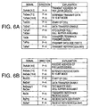
- TxPrty is an odd parity signal for the transmit data signal TxData, and is sent to the PHY layer devices 17-1 from the ATM layer device 17-2.
- TxRef is a reference signal, which is sent to the PHY layer devices 17-1 from the ATM layer device 17-2.
- RxData is a receive data signal which the ATM layer device 17-1 receives from the PHY layer devices 17-1.
- the signal RxData occupies eight receive data bus lines [7:0] in the 8-bit mode, and further uses extended data bus lines RxData [15:8] in the 16-bit mode.
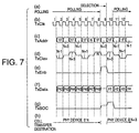
- Fig. 7 is a timing chart of the transmit operation in the Level 2 UTOPIA interface.
- cell data is transferred from the ATM layer device to the PHY layer device.
- the ATM layer device In response to TxClk9, as shown in part (e) of Fig. 7, the ATM layer device sends out the transfer enable signal TxEnb* (switches to the low level). Then, as shown in part (f) of Fig. 7, the next cell is sent out in the order of headers H1, H2, H3 and H4. Also, the signal TxSOC indicative of start of cell is sent out as shown in part (g) of Fig. 7.
- the polling operation commences sending, as the receive address signal RxAddr, the address of the PHY layer device which is a candidate for the next receive source from which cell will be received.
- the PHY layer device specified by the above address signal sends out the signal RxClav during the next clock cycle, and thus informs the ATM layer device of the state of a cell send-out buffer of the above PHY layer device.
- the ATM layer device recognizes that the cell send-out buffer of the (N-1)th PHY layer device cannot be used.
- the ATM layer device selects the address of the (N+3)th PHY layer device, which sends out, in the next clock cycle, that is, in response to RxClk3, a signal indicating that the cell send-out buffer is available (the signal is switched to the high level).
- the ATM layer device recognizes that the cell send-out buffer of the (N+3)th PHY layer device is available.
- the (N+3)th PHY layer device detects that the transfer enable signal RxEnb* for receive cell is stopped in response to RxClk9 (switches to the high level) and the address signal of the (N+3)th PHY layer device is sent out as the address signal, and recognizes that sending out of its own cell data is started. Then, the (N+3)th PHY layer device sends out cell data to the receive data signal line RxData.
- the ATM layer device sends out the receive cell transfer enable signal RxEnb* (switches to the low level), and the PHY layer device #N+3 detects that the receive transfer enable signal RxEnb* is sent out in response to RxClk10. Then, as shown in part (f) of Fig. 8, the cell is sent out in the order of headers H1, H2, H3 and H4. Also, the signal RxSOC indicative of start of cell is switched to the high level as shown in part (g) of Fig. 8.
- the PHY layer device #N+3 thus selected sends, as cell data, cell to the receive data signal line during the time when the receive cell transfer enable signal RxEnB* is being sent out (as long as it is at the low level). Further, during the above period, the polling is started again in synchronism with RxClk10 (which denotes the tenth rising edge of the receive clock signal RxClk).
- the Level 2 UTOPIA interface uses the 5-bit address signal, and required one of the five bits to be null.
- the upper limit on the number of PHY layer devices that can be connected to the ATM layer device is equal to 31.
- a large-scale access network apparatus required to accommodate a large number of subscribers is required that PHY layer devices over than the upper limit be connected to the ATM layer device.
- an ATM apparatus In order to configure an ATM apparatus using PHY layer devices which conform with the Level 2 UTOPIA interface, such as an access network device capable of multiplexing and demultiplexing ATM cells, it is required to connect PHY layer devices in a multistage formation and enable a large number of PHY layer devices to be accommodated. Additionally, if a package which handles multiplexing and demultiplexing is segmented into parts of an appropriate size and such parts are connected in the multistage formation, an ATM apparatus having an appropriate scale can be constructed economically.
- the ATM apparatus may be configured so that the address signal and the data signal form a routing information field in which arbitrary information other than the routing information can be stored. Hence, desired information can easily be transferred to another device.
- the ATM apparatus may be configured so that the address signal and the data signal form a routing information field in which arbitrary information other than the routing information can be stored, the arbitrary information being transferred between the ATM device and the devices of the lowermost stage of the multistage formation. Hence desired information can be transferred to another device with ease.
- the ATM apparatus may be configured so that the given interface is a Level 2 UTOPIA interface.
- the given field is a user defined field of the Level 2 UTOPIA interface.
- the ATM device is an ATM layer device of the Level 2 UTOPIA interface, and the devices arranged in the multistage formation are respectively physical layer devices of the Level 2 UTOPIA interface.
- Another object of the present invention is to provide an ATM device applicable to an ATM apparatus including a plurality of devices arranged in a multistage formation in which the ATM device is located at a top of the multistage structure, wherein the ATM device and the plurality of devices employ a given interface using an address signal and a control signal,
- the ATM device comprises: an ATM switch which switches an ATM cell; and a routing table that stores routing information with regard to a value of a VPI/VCI field provided in a header of the ATM cell, the routing information including address information concerning at least one of the devices by using the address signal and a data signal written into a given field of the ATM cell.
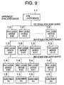
- Fig. 9 is a block diagram of an ATM apparatus having a multistage connection formation according to an embodiment of the present invention.
- the ATM apparatus shown in Fig. 9 includes an ATM layer device 1-1, PHY layer devices 1-2 of the first stage, PHY layer devices 1-3 of the second stage, PHY layer devices 1-4 of the third stage, and subscriber terminals 1-5 of the fourth stage.
- the ATM layer device 1-1 is located at the uppermost stage, and more particularly corresponds to an ATM switch (a switch chip).
- the PHY layer stages 1-2, 1-3 and 1-4 located at lower stages correspond to cell multiplexing/demultiplexing devices.
- the subscriber terminals 1-5 are accommodated by the PHY layer devices 1-4 of the lowermost stage.
- the PHY layer devices 1-2, 1-3 and 1-4 of the first, second and third stages are coupled with the ATM layer device 1-1 through the Level 2 UTOPIA interface.
- the Level 2 UTOPIA interface defines the transmit address signal TxAddr consisting of 5 bits and the receive address signal RxAddr consisting of 5 bits.
- the PHY layer device in each stage latches cell data by referring to the address described in the routing information field, and transfers the latched cell data to the PHY layer device of the just lower stage while shifting the routing information.
- the PHY layer devices of the lower stages are not equipped with routing tables and do not refer to the VPI/VCI field of the cell header but performs routing based on only the address information described in the routing information field.
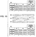
- Fig. 10 shows an example of the routing table and an example of the routing information field employed in the present embodiment. More particularly, part (A) of Fig. 10 shows a routing table used in the 8-bit mode.
- the routing table shown in part (A) of Fig. 10 is equipped with a routing information field which stores, with respect to the value of the VPI/VCI field of the cell header, routing information which includes chained address information concerning up to the destination (that is, the destination PHY layer device and intervening PHY devices).
- the uppermost-stage ATM layer device refers to the routing table, and reads, from the value of the VPI/VCI field of the cell header, the corresponding routing information. For example, referring to part (A) of Fig. 10, the ATM layer device reads, from the value of the VPI/VCI field with regard to subscriber #3 '00000001/00000000 00001010', the address of the PHY layer device '00100 10110011'.
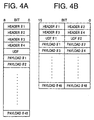
- the uppermost ATM layer device writes the first 5 bits of the routing information into the transmit address signal TxAddr, and writes the remaining 8 bits thereof into the user defined field UDF. Then, the uppermost ATM layer device sends out the cell data including such routing information to the first-stage PHY layer devices 1-2.
- Part (B) of Fig. 10 indicates routing information sent out by the uppermost ATM layer device 11-1.
- PHY layer device #001 of the first stage is selected. Then, PHY layer device #001 of the first stage extracts the routing information from the address signal TxAddr and the user defined field UDF, and shifts leftwards the address information by three bits, as shown in part (C) of Fig. 10. The resultant address information obtained by the three-bit leftward shift operation is output to the PHY layer devices of the second stage.
- PHY layer device #011 of the third stage is selected. Then, cell data is sent from PHY layer device #011 to subscriber terminal #3.
- the uppermost ATM layer device 1-1 writes information indicative of multicasting into the routing information field, which is sent to the PHY layer devices of the stages.
- Each of the PHY layer devices receives the information indicative of multicasting and thus make a copy of the ATM cell.
- the traffic (the number of cells passing) of the uppermost ATM layer device can be reduced and efficient multicasting can be realized.
- Part (E) of Fig. 11 shows an example of the contents of the routing information field of the receive operation at the time of multicasting.
- the uppermost-stage ATM layer device receives routing information '1100000000000' inserted into the routing information field, the above routing information being originated from the cell transmit source PHY layer device.
- PVC permanent virtual channel
- SVC switched virtual channel
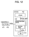
- Fig. 12 shows a routing table setting method associated with the permanent virtual channel.
- Fig. 12 shows a terminal device 4-1 in subscriber home #1, a network termination equipment 4-2, an access network device 4-3 installed in an office station, a routing table 4-31, an operating system part (Ops) 4-4, and an ATM switch device 4-5.
- Ops operating system part
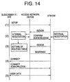
- Fig. 13 shows a routing table setting method associated with the switched virtual channel (SVC).
- Fig. 13 shows a terminal device 5-1 in subscriber home #1, a network termination equipment 5-2, an access network device 5-3 installed in an office station, a routing table 5-31, an operating system part (Ops) 5-4, and an ATM switch device 5-5.
- SVC switched virtual channel
- the switched virtual channel is not permanently assigned as in the case of the permanent virtual channel, but is newly assigned each time a call from a subscriber is issued.
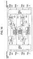
- the user defined field extracting part 7-2 extracts the user defined field UDF, and extracts the routing information from the receive address signal RxAddr and the user defined field UDF.
- the routing information may include other information transferred from a PHY layer device of a lower stage in addition to the routing information.
- the information included in the routing information can be read from the value of the VPC/VCI extracted by the VPI/VCI check part 7-3.
- the routing information delete and shift part 8-11 deletes and discards only three upper bits of the routing information used for routing at the upper stage, and shifts the remaining bits towards the upper side by three bits. Then, the part 8-11 sends out the five upper bits of the shifted routing information to the PHY layer devices of the lower stage via the Level 2 UTOPIA interface part 8-1 connected to the lower stage and the transmit address signal line TxAddr. Further, the part 8-11 outputs the remaining bits of the routing information to the user defined field inserting part 8-8 involved with transmit operation.
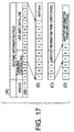
- the routing information is reproduced as shown in parts (C) and (D) of Fig. 17 by the user defined field extracting part 8-2 involved with receive operation, the routing information write shift part 8-9 and the user defined field inserting part 8-3 involved with receive operation. Then, the ATM cell is transferred to the PHY layer device of the upper stage via the ATM cell FIFO buffer 8-4 involved with receive operation and the Level 2 UTOPIA interface part 8-5 connected to the upper stage.
- an ATM cell received via the Level 2 UTOPIA interface part 10-4 connected to the upper stage is temporarily stored in the ATM cell FIFO buffer 10-5 involved with transmit operation. Then, the routing information is extracted from the ATM cell by the user defined field extracting part 10-6, and the extracted routing information is applied to the routing information reproducing and processing part 10-10.
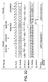
- Device #3 extracts a data signal of the user defined field UDF in synchronism with the rising edge of clock 14. Then device #3 extracts the routing information by using the already extracted transmit address signal TxAddr and the data signal of the user defined field UDF.
Landscapes
- Engineering & Computer Science (AREA)
- Computer Networks & Wireless Communication (AREA)
- Signal Processing (AREA)
- Data Exchanges In Wide-Area Networks (AREA)
- Communication Control (AREA)
Applications Claiming Priority (2)
| Application Number | Priority Date | Filing Date | Title |
|---|---|---|---|
| JP06518798A JP3911655B2 (ja) | 1998-03-16 | 1998-03-16 | Atm装置 |
| JP6518798 | 1998-03-16 |
Publications (3)
| Publication Number | Publication Date |
|---|---|
| EP0944286A2 true EP0944286A2 (de) | 1999-09-22 |
| EP0944286A3 EP0944286A3 (de) | 2000-04-05 |
| EP0944286B1 EP0944286B1 (de) | 2005-11-23 |
Family
ID=13279679
Family Applications (1)
| Application Number | Title | Priority Date | Filing Date |
|---|---|---|---|
| EP99104037A Expired - Lifetime EP0944286B1 (de) | 1998-03-16 | 1999-03-16 | Vorrichtung für Asynchronen transfer mode |
Country Status (4)
| Country | Link |
|---|---|
| US (1) | US6693911B2 (de) |
| EP (1) | EP0944286B1 (de) |
| JP (1) | JP3911655B2 (de) |
| DE (1) | DE69928464T2 (de) |
Cited By (4)
| Publication number | Priority date | Publication date | Assignee | Title |
|---|---|---|---|---|
| WO2001093511A1 (de) * | 2000-05-26 | 2001-12-06 | Ericsson Ahead Communications Systems Gmbh | System zur übertragung von daten |
| AU2002301534B2 (en) * | 2001-10-29 | 2004-09-02 | Samsung Electronics Co., Ltd. | Data translation apparatus of ATM in mobile communication system |
| CN100359898C (zh) * | 2002-06-27 | 2008-01-02 | 中兴通讯股份有限公司 | 多路复用接收受控器 |
| CN100393053C (zh) * | 2002-06-27 | 2008-06-04 | 中兴通讯股份有限公司 | 多路解复用发送受控器 |
Families Citing this family (13)
| Publication number | Priority date | Publication date | Assignee | Title |
|---|---|---|---|---|
| WO2000079828A1 (en) * | 1999-06-17 | 2000-12-28 | Nokia Corporation | Multiplexing and demultiplexing method and apparatus |
| WO2001026307A1 (en) * | 1999-10-05 | 2001-04-12 | Thomson Licensing S.A. | Messaging services for a digital subscriber loop |
| US6952420B1 (en) * | 1999-10-18 | 2005-10-04 | Paradyne Corporation | System and method for polling devices in a network system |
| KR100308907B1 (ko) * | 1999-11-15 | 2001-11-02 | 윤종용 | 저속 가입자 확장형 시스템 |
| FI109315B (fi) * | 1999-12-28 | 2002-06-28 | Nokia Corp | Yhteyden järjestäminen verkkoelementissä |
| KR20010105690A (ko) * | 2000-05-17 | 2001-11-29 | 박종섭 | 기지제어국 시스템의 에이티엠 셀 버스 스위칭 장치 |
| BR0111453A (pt) * | 2000-06-08 | 2003-06-24 | Thomson Licensing Sa | Multidifusão de atm para a liberação de informações por uma rede |
| KR20020084355A (ko) * | 2001-04-30 | 2002-11-07 | 현대네트웍스 주식회사 | 8 포트 vdsl 가입자 인터페이스 장치 |
| US6850526B2 (en) * | 2001-07-06 | 2005-02-01 | Transwitch Corporation | Methods and apparatus for extending the transmission range of UTOPIA interfaces and UTOPIA packet interfaces |
| JP3771153B2 (ja) * | 2001-08-29 | 2006-04-26 | 三菱電機株式会社 | Utopiaインタフェース制御装置及び方法並びに該装置に用いるバックワイヤボード |
| TW527796B (en) * | 2001-08-30 | 2003-04-11 | Tailyn Comm Co Ltd | ATM communication system for improving UTOPIA communication interface and method therefor |
| US7016947B1 (en) * | 2001-12-14 | 2006-03-21 | Cisco Technology, Inc | Convenient configuration of an identifier of a segment of a virtual circuit |
| CA2386453A1 (en) * | 2002-05-15 | 2003-11-15 | Catena Networks Canada Inc. | Higher layer bonding of multiple access lines for carrier grade access |
Family Cites Families (12)
| Publication number | Priority date | Publication date | Assignee | Title |
|---|---|---|---|---|
| JP2763073B2 (ja) | 1988-01-26 | 1998-06-11 | 富士通株式会社 | 自己ルーティング通話路制御方式 |
| JP2670073B2 (ja) | 1988-03-19 | 1997-10-29 | 富士通株式会社 | 自己ルーチング交換方式 |
| JPH01289342A (ja) | 1988-05-17 | 1989-11-21 | Fujitsu Ltd | 自己ルーティング交換方式 |
| JPH03207140A (ja) | 1990-01-09 | 1991-09-10 | Fujitsu Ltd | 非同期転送モード用交換機 |
| JPH07264214A (ja) * | 1994-02-07 | 1995-10-13 | Fujitsu Ltd | インターフェース装置 |
| US5485456A (en) * | 1994-10-21 | 1996-01-16 | Motorola, Inc. | Asynchronous transfer mode (ATM) system having an ATM device coupled to multiple physical layer devices |
| CA2181293C (en) * | 1995-07-17 | 2000-06-06 | Charles Kevin Huscroft | Atm layer device |
| US5724358A (en) * | 1996-02-23 | 1998-03-03 | Zeitnet, Inc. | High speed packet-switched digital switch and method |
| US5812527A (en) * | 1996-04-01 | 1998-09-22 | Motorola Inc. | Simplified calculation of cell transmission rates in a cell based netwook |
| US5878045A (en) * | 1996-04-26 | 1999-03-02 | Motorola, Inc. | Method and apparatus for converting data streams in a cell based communications system |
| KR0169247B1 (ko) * | 1996-08-09 | 1999-02-01 | 양승택 | 에스티엠 기반 에이티엠 셀 물리계층 처리회로 |
| JP3207140B2 (ja) | 1996-10-18 | 2001-09-10 | みかど化工株式会社 | 遮光ネット |
-
1998
- 1998-03-16 JP JP06518798A patent/JP3911655B2/ja not_active Expired - Fee Related
-
1999
- 1999-03-16 US US09/270,326 patent/US6693911B2/en not_active Expired - Fee Related
- 1999-03-16 DE DE1999628464 patent/DE69928464T2/de not_active Expired - Lifetime
- 1999-03-16 EP EP99104037A patent/EP0944286B1/de not_active Expired - Lifetime
Cited By (4)
| Publication number | Priority date | Publication date | Assignee | Title |
|---|---|---|---|---|
| WO2001093511A1 (de) * | 2000-05-26 | 2001-12-06 | Ericsson Ahead Communications Systems Gmbh | System zur übertragung von daten |
| AU2002301534B2 (en) * | 2001-10-29 | 2004-09-02 | Samsung Electronics Co., Ltd. | Data translation apparatus of ATM in mobile communication system |
| CN100359898C (zh) * | 2002-06-27 | 2008-01-02 | 中兴通讯股份有限公司 | 多路复用接收受控器 |
| CN100393053C (zh) * | 2002-06-27 | 2008-06-04 | 中兴通讯股份有限公司 | 多路解复用发送受控器 |
Also Published As
| Publication number | Publication date |
|---|---|
| JPH11266250A (ja) | 1999-09-28 |
| EP0944286B1 (de) | 2005-11-23 |
| EP0944286A3 (de) | 2000-04-05 |
| JP3911655B2 (ja) | 2007-05-09 |
| US6693911B2 (en) | 2004-02-17 |
| US20030086429A1 (en) | 2003-05-08 |
| DE69928464T2 (de) | 2006-08-03 |
| DE69928464D1 (de) | 2005-12-29 |
Similar Documents
| Publication | Publication Date | Title |
|---|---|---|
| EP0944286B1 (de) | Vorrichtung für Asynchronen transfer mode | |
| US5852606A (en) | Method and apparatus for transmitting cells across an ATM switch bus | |
| US5809024A (en) | Memory architecture for a local area network module in an ATM switch | |
| CA2020244C (en) | Packet switch network for communication using packet having virtual connection identifier vci | |
| KR960003505B1 (ko) | 에이티엠(atm) 다중화 처리 장치 | |
| EP0700229B1 (de) | Verbindungsloses Kommunikationssystem, Testmethode und Intra-Station-Steuerungssystem | |
| KR100292191B1 (ko) | 스위칭시스템 | |
| US5737334A (en) | Pipeline architecture for an ATM switch backplane bus | |
| EP0909108A2 (de) | Verfahren und Vorrichtung zur Anpassung von ATM-Anpassungsschichtsformaten | |
| US20040125809A1 (en) | Ethernet interface over ATM Cell, UTOPIA xDSL in single and multiple channels converter/bridge on a single chip and method of operation | |
| JPH0715435A (ja) | 非同期転送モード交換装置 | |
| KR19980063448A (ko) | 라인 어댑터에 대한 부착을 허용하는 분산 엘리먼트를 구비하고 멀티캐스팅 능력을 가진 스위칭 시스템 | |
| EP0978181A1 (de) | Übertragung von atm zellen | |
| KR20010005539A (ko) | 통신용 다중-서비스 회로 | |
| CN1289488A (zh) | 具有基于atm连接方案的移动通信系统 | |
| US5970068A (en) | Telecommunication system with transport protocol device for mixing asynchronous signaling traffic with TDM traffic on a TDM backbone | |
| KR100292192B1 (ko) | 라인어댑터에대한부착을허용하는분산엘리먼트를구비한스위칭시스템 | |
| US6128299A (en) | System for low-cost connection of devices to an ATM network | |
| JPH09181726A (ja) | Atmネットワークで接続を結合する方法及びシステム | |
| JP3955640B2 (ja) | ポイント対ポイント・インタフェース上にポイント対マルチポイント・インタフェースを再構築する方法 | |
| JP3070545B2 (ja) | パケット通信網及びパケット交換機 | |
| JPH10210045A (ja) | ATM−Uバス方式ならびに該方式に用いる分岐装置およびATM155Mbpsインタフェース | |
| Kesselring | An Overview of Interconnecting LANs over ATM," | |
| KR20000046347A (ko) | 수요밀집형 광가입자 전송장치에서의 비동기전송모드 셀 헤더변환 및 경로 제어장치 | |
| JPH05183574A (ja) | セル交換装置 |
Legal Events
| Date | Code | Title | Description |
|---|---|---|---|
| PUAI | Public reference made under article 153(3) epc to a published international application that has entered the european phase |
Free format text: ORIGINAL CODE: 0009012 |
|
| AK | Designated contracting states |
Kind code of ref document: A2 Designated state(s): DE FR GB |
|
| AX | Request for extension of the european patent |
Free format text: AL;LT;LV;MK;RO;SI |
|
| PUAL | Search report despatched |
Free format text: ORIGINAL CODE: 0009013 |
|
| AK | Designated contracting states |
Kind code of ref document: A3 Designated state(s): AT BE CH CY DE DK ES FI FR GB GR IE IT LI LU MC NL PT SE |
|
| AX | Request for extension of the european patent |
Free format text: AL;LT;LV;MK;RO;SI |
|
| 17P | Request for examination filed |
Effective date: 20000505 |
|
| AKX | Designation fees paid |
Free format text: DE FR GB |
|
| 17Q | First examination report despatched |
Effective date: 20030613 |
|
| GRAP | Despatch of communication of intention to grant a patent |
Free format text: ORIGINAL CODE: EPIDOSNIGR1 |
|
| GRAS | Grant fee paid |
Free format text: ORIGINAL CODE: EPIDOSNIGR3 |
|
| GRAA | (expected) grant |
Free format text: ORIGINAL CODE: 0009210 |
|
| AK | Designated contracting states |
Kind code of ref document: B1 Designated state(s): DE FR GB |
|
| REG | Reference to a national code |
Ref country code: GB Ref legal event code: FG4D |
|
| REF | Corresponds to: |
Ref document number: 69928464 Country of ref document: DE Date of ref document: 20051229 Kind code of ref document: P |
|
| ET | Fr: translation filed | ||
| PLBE | No opposition filed within time limit |
Free format text: ORIGINAL CODE: 0009261 |
|
| STAA | Information on the status of an ep patent application or granted ep patent |
Free format text: STATUS: NO OPPOSITION FILED WITHIN TIME LIMIT |
|
| 26N | No opposition filed |
Effective date: 20060824 |
|
| PGFP | Annual fee paid to national office [announced via postgrant information from national office to epo] |
Ref country code: FR Payment date: 20100324 Year of fee payment: 12 |
|
| PGFP | Annual fee paid to national office [announced via postgrant information from national office to epo] |
Ref country code: GB Payment date: 20100310 Year of fee payment: 12 |
|
| PGFP | Annual fee paid to national office [announced via postgrant information from national office to epo] |
Ref country code: DE Payment date: 20100422 Year of fee payment: 12 |
|
| GBPC | Gb: european patent ceased through non-payment of renewal fee |
Effective date: 20110316 |
|
| REG | Reference to a national code |
Ref country code: FR Ref legal event code: ST Effective date: 20111130 |
|
| PG25 | Lapsed in a contracting state [announced via postgrant information from national office to epo] |
Ref country code: FR Free format text: LAPSE BECAUSE OF NON-PAYMENT OF DUE FEES Effective date: 20110331 Ref country code: DE Free format text: LAPSE BECAUSE OF NON-PAYMENT OF DUE FEES Effective date: 20111001 |
|
| REG | Reference to a national code |
Ref country code: DE Ref legal event code: R119 Ref document number: 69928464 Country of ref document: DE Effective date: 20111001 |
|
| PG25 | Lapsed in a contracting state [announced via postgrant information from national office to epo] |
Ref country code: GB Free format text: LAPSE BECAUSE OF NON-PAYMENT OF DUE FEES Effective date: 20110316 |