EP0944923B1 - Nnn/ppp logische anordnungen mit ultraniedrigem leistungs-verzögerungsprodukt - Google Patents
Nnn/ppp logische anordnungen mit ultraniedrigem leistungs-verzögerungsprodukt Download PDFInfo
- Publication number
- EP0944923B1 EP0944923B1 EP97937075A EP97937075A EP0944923B1 EP 0944923 B1 EP0944923 B1 EP 0944923B1 EP 97937075 A EP97937075 A EP 97937075A EP 97937075 A EP97937075 A EP 97937075A EP 0944923 B1 EP0944923 B1 EP 0944923B1
- Authority
- EP
- European Patent Office
- Prior art keywords
- channel region
- semiconductor device
- source
- region
- oxide layer
- Prior art date
- Legal status (The legal status is an assumption and is not a legal conclusion. Google has not performed a legal analysis and makes no representation as to the accuracy of the status listed.)
- Expired - Lifetime
Links
Images


Classifications
-
- H—ELECTRICITY
- H10—SEMICONDUCTOR DEVICES; ELECTRIC SOLID-STATE DEVICES NOT OTHERWISE PROVIDED FOR
- H10D—INORGANIC ELECTRIC SEMICONDUCTOR DEVICES
- H10D30/00—Field-effect transistors [FET]
- H10D30/60—Insulated-gate field-effect transistors [IGFET]
- H10D30/67—Thin-film transistors [TFT]
- H10D30/674—Thin-film transistors [TFT] characterised by the active materials
- H10D30/6741—Group IV materials, e.g. germanium or silicon carbide
- H10D30/6743—Silicon
- H10D30/6744—Monocrystalline silicon
-
- H—ELECTRICITY
- H10—SEMICONDUCTOR DEVICES; ELECTRIC SOLID-STATE DEVICES NOT OTHERWISE PROVIDED FOR
- H10D—INORGANIC ELECTRIC SEMICONDUCTOR DEVICES
- H10D30/00—Field-effect transistors [FET]
- H10D30/60—Insulated-gate field-effect transistors [IGFET]
- H10D30/637—Lateral IGFETs having no inversion channels, e.g. buried channel lateral IGFETs, normally-on lateral IGFETs or depletion-mode lateral IGFETs
-
- H—ELECTRICITY
- H10—SEMICONDUCTOR DEVICES; ELECTRIC SOLID-STATE DEVICES NOT OTHERWISE PROVIDED FOR
- H10D—INORGANIC ELECTRIC SEMICONDUCTOR DEVICES
- H10D30/00—Field-effect transistors [FET]
- H10D30/60—Insulated-gate field-effect transistors [IGFET]
- H10D30/67—Thin-film transistors [TFT]
- H10D30/674—Thin-film transistors [TFT] characterised by the active materials
- H10D30/6741—Group IV materials, e.g. germanium or silicon carbide
- H10D30/6743—Silicon
-
- H—ELECTRICITY
- H10—SEMICONDUCTOR DEVICES; ELECTRIC SOLID-STATE DEVICES NOT OTHERWISE PROVIDED FOR
- H10D—INORGANIC ELECTRIC SEMICONDUCTOR DEVICES
- H10D84/00—Integrated devices formed in or on semiconductor substrates that comprise only semiconducting layers, e.g. on Si wafers or on GaAs-on-Si wafers
- H10D84/80—Integrated devices formed in or on semiconductor substrates that comprise only semiconducting layers, e.g. on Si wafers or on GaAs-on-Si wafers characterised by the integration of at least one component covered by groups H10D12/00 or H10D30/00, e.g. integration of IGFETs
- H10D84/82—Integrated devices formed in or on semiconductor substrates that comprise only semiconducting layers, e.g. on Si wafers or on GaAs-on-Si wafers characterised by the integration of at least one component covered by groups H10D12/00 or H10D30/00, e.g. integration of IGFETs of only field-effect components
- H10D84/83—Integrated devices formed in or on semiconductor substrates that comprise only semiconducting layers, e.g. on Si wafers or on GaAs-on-Si wafers characterised by the integration of at least one component covered by groups H10D12/00 or H10D30/00, e.g. integration of IGFETs of only field-effect components of only insulated-gate FETs [IGFET]
- H10D84/85—Complementary IGFETs, e.g. CMOS
-
- H—ELECTRICITY
- H10—SEMICONDUCTOR DEVICES; ELECTRIC SOLID-STATE DEVICES NOT OTHERWISE PROVIDED FOR
- H10D—INORGANIC ELECTRIC SEMICONDUCTOR DEVICES
- H10D86/00—Integrated devices formed in or on insulating or conducting substrates, e.g. formed in silicon-on-insulator [SOI] substrates or on stainless steel or glass substrates
- H10D86/201—Integrated devices formed in or on insulating or conducting substrates, e.g. formed in silicon-on-insulator [SOI] substrates or on stainless steel or glass substrates the substrates comprising an insulating layer on a semiconductor body, e.g. SOI
Definitions
- This invention is directed to very thin gate oxide semiconductor devices having source, drain and channel regions all doped with dopants of the same conductivity type, and to complementary devices in which the three regions of one device are all of the same conductivity type, but opposite to the conductivity type of the three regions of the other device.
- CMOS transistors have source and drain regions of the same conductivity type with a channel region between of the opposite conductivity type.
- one transistor is a npn device and the complementary transistor is a pnp type.
- These devices have a threshold voltage which is typically about 500 to 1500 millivolts.
- the capacitance of such devices is high due in part to an oxide layer of about 10 to 50 nm (100 to 500 Angstroms ( ⁇ )) in thickness insulating the gate electrode from the channel region. Since the power required by these devices and their switching speed are both direct functions of the capacitance and threshold voltage, they are relatively power hungry and slow for certain applications.
- HTSC high temperature superconducting
- JP 02-234461 describes a CMOS device constructed of an n-type channel MOS formed on an n-type well and a p-type channel MOS formed on a p-type well. The device is intended generally for low threshold operation at low temperature.
- the article entitled 'A High Performance Low Temperature 0.3 ⁇ m CMOS on SIMOX' by G.G. Shahidi et al. 1992 Symposium on VLSI Technology Digest of Papers, pp. 106-7, 2 June 1992 describes a CMOS device fabricated on a thin SIMOX film to reduce the device threshold voltage.
- a film thickness of 40 nm for a doping of 1 x 10E17 charges/cm 3 .
- the gate oxide film is described as having a thickness of 7nm.
- the invention is directed to a semiconductor device comprising a substrate, an active layer on the substrate having spaced apart source and drain regions, both of the same conductivity type, and a channel region between the source and drain regions, also of the same conductivity type.
- a key feature is that the channel region is no more than about 30 nm (300 ⁇ ) thick and in all cases less than the Debye length associated with a predetermined dopant level of the channel region.
- the thickness of the channel region is preferably only about 10nm (100 ⁇ ) thick.
- An oxide layer is provided between the channel region and a gate electrode.
- this oxide layer is no more than about 2 nm (20 ⁇ ) thick, and preferably between about 0.5 and 1 nm (5 and 10 ⁇ ) in thickness.
- the devices are adapted for operation at temperatures which pin the Fermi level near or at the majority dopant level, thus, temperatures from less than about 150°K to about 77°K.
- Electrodes are also provided for the source and drain regions. Complementary devices may be provided by one such device in which the source, channel, drain regions are N+, N, N+ and an adjacent P+, P, P+ device.
- an oxide layer is provided between the substrate and the active layer to more easily establish the thickness of channel region.
- the active layer is silicon, although other materials with MOS properties such as silicon carbide, and gallium arsenide can be used.
- doped polysilicon can be used in place of metal for the electrodes, including the gate electrode.
- the thinness of the channel region between the source and drain keeps the current which flows at a zero value of gate voltage to a minimum. It can be shown that ON/OFF ratios of 100 or more can be easily met by a combination of a 20nm (200 ⁇ ) thick channel region between the source and drain regions and the fact that a small reverse bias on the gate electrode (a few millivolts) depletes the channel in the channel region completely, forcing the current to near zero at the origin of the VI (voltage/current) curve.
- the channel region has a dopant - thickness product of about 3 to 10E10 charges/cm 2 .
- the length of the channel region, between the source and drain regions is from about 50 nm (500 ⁇ ) to 250 nm (2500 ⁇ ) and preferably about 125 nm (1250 ⁇ ).
- CMOS device 1 such as shown in Figure 1.
- This device 1 includes an npn transistor 3 formed by N+ source and drain regions 5 and 7 and a P region 9.
- a thin oxide layer 11 extends over the source, channel and drain regions. Typically, this oxide layer 11 is 10 nm (100 ⁇ ) to 50 nm (500 ⁇ ) thick.
- a metal or polysilicon gate electrode 13 is isolated from the channel region 9 by the oxide layer 11. Source and drain electrodes 15 and 17, respectively, are positioned through the oxide layer 11 over the source and drain regions.
- a complementary PNP transistor 19 adjacent to the end NPN transistor 3 includes P+ source region 21 and drain region 23 separated by an N type substrate 25.
- the oxide layer 11 extends over these regions and insulates a gate electrode 27 from the channel region formed by the substrate 25. Electrodes 29 and 31 positioned through the oxide layer 11 form source and drain electrodes, respectively.
- Figure 2 is a Fermi diagram for the NPN transistor portion of Figure 1. In this diagram, E c is the conduction band, E v is the valence band, E d is the donor level, and E f is the Fermi level.
- the p doping of the p region 9 in the NPN device 3 leads to a high threshold voltage shown by the fact that the onset of current requires that the conduction and valence bands bend as indicated at point 33 by 2 ⁇ p which is typically about 0.5 to 0.75 volts.
- this high turn-on gate voltage makes the device 3 power hungry and slow, since the gate capacitance has to be charged up to an order of 2 ⁇ p volts.
- a complementary device 35 includes an NNN transistor 37 and a PPP transistor 39 formed side- by-side in an active layer 41 formed on a substrate 43.
- an oxide layer 45 is provided between the substrate 43 and the active layer 41.
- the NNN device 37 is formed by an N + source region 47 and an N + drain region 49 spaced apart in the active layer 41 by the N channel region 51.
- a thin oxide layer 53 insulates a gate electrode 55 from the channel region 51.
- the oxide layer 53 also extends over the source and drain regions 47 and 49 where source and drain contacts 57 and 59, are formed, respectively.
- the PPP device 39 includes a P + source region 61 and a P + drain region 63 in the active layer 41 separated by a P channel region 65.
- a thin oxide layer 67 insulates a gate electrode 69 from the channel region 65 and extends across the source and drain region 61 and 63 where a source electrode contact 71 and a drain electrode contact 73 are formed.
- the channel regions 51 and 65 are very thin; namely, only about 30 nm (300 ⁇ ), but even about 10 nm (100 ⁇ ).
- the oxide layers 53 and 67 are also very thin; namely not more than about 2 nm (20 ⁇ ) and preferably 0.5 to 1 nm (5 to 10 ⁇ ).
- the length of the channel regions 51 and 65, between the source and drain regions is between about 50 to 250 nm (500 to 2500 ⁇ ) and preferably about 50 to 150 nm (500 to 1500 ⁇ ) with 125 nm (1250 ⁇ ) being suitable.
- the active layer 41 is silicon into which the source and drain region are diffused and separated by photolithography techniques to form the channel regions.
- other materials exhibiting MOS activity such as silicon carbide and gallium arsenide could be utilized.
- the source and drain regions 49, 63 and 47, 61 in the illustrative device are doped to about 1E20 charges/cm 3 .
- the channel regions 51 and 65 can be doped to levels of about 1E+16 charges per cm 3 to produce dopant-thickness products in the range of about 3 to about 30 E+ 10 charges per cm 2 .
- the voltage drop required to move the Fermi level E f to the onset of conduction E c does not contain the2 ⁇ voltage term.
- the Fermi level at 77K just about sits on the donor level E d , which is only about 50 milli-electron volts away from the conduction band E c for phosphorous as can be seen in Figure 5 at the point 75 for the 1E + 16 dopant curve 77.
- the temperature is used to pin the Fermi level E g near or at the majority dopant level E d in Figure 4, a known small distance from the majority carrier band edge where it is ready to cause conduction with the smallest of applied surface fields.
- the onset of gate voltage for conduction is then the band bending at 79 which is equal to about E d /2 volts, a much smaller value than the2 ⁇ volts required by the conventional CMOS devices as shown in Figure 2.
- V T 2 ⁇ Fo + Q SC C or + ' ⁇ V WF
- the first term is the band bending voltage drop which for an NPN transistor is about 0.8 volts.
- the second term is the space charge voltage drop which is typically about 1 volt.
- the final term is the work function difference voltage drop which can be made negligible with proper adjustment of the gate metal or polysilicon work function.
- the threshold voltage for the typical conventional MOS device can be as high as about 1.8 volts.
- Equation 2 Comparing Equation 2, to Equation 1 above, it can be seen that the second and third terms of Equation 1 are absent in an NNN or PPP device and the first term, 2 ⁇ of Equation 1, is replaced in Equation 2 by only the minuscule band bending associated with the small movement of the Fermi level from E d to the conduction band edge E c , a few tens of millivolts. It should be noted that the imposition of the oxide layer 53, 67 between the gate 55, 69 and the channel region 51, 65 usually doubles this contribution for oxides as thin as 2 nm (20 ⁇ ) or so. Thicker oxide layers can be deleterious to a small threshold voltage.
- Equation 1 drives the turn-on voltage of the conventional thick channel region NPN device, curve 85, to the right in Figure 6b resulting in a difference in threshold voltage of about 880 millivolts, even with a 2 nm (20 ⁇ ) thin oxide in the NPN device. This essentially ruins the NPN/PNP system for being able to achieve 100 millivolt supply voltage logic.
- Figure 7 which is a plot of the electron concentration versus temperature for three levels of doping of the channel region, deals briefly with the fact that at 77K, 1E16/cm 3 material shown by the trace 87 partially deionizes at the point 89. This helps in two ways: 1) it is this deionization which helps pin the Fermi level near E d , close to the conduction band edge "ready to go", 2) the channel region 51 in Figure 3 is now less conducting, raising the on-to-off ratio of the device.
- the threshold voltage of the NNN devices becomes rather insensitive to both the thickness of layer 41 and its exact n doping level. This makes the device significantly easier to fabricate reproducibly than might be expected from fabrication of thick channel bulk region MOS devices ( ⁇ 1000 ⁇ +) presently known to the art.
- F f oper ⁇ g m 2 ⁇ C 36 GHZ
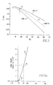
- Figure 8 illustrates competitive P x TAU products for other devices.
- CMOS 91 and cooled CMOS 93 have P x TAU products of about 1 to 2E-13 joules
- the logic proposed herein 95 has P x TAU products, assuming a fan out of 3, of 2E-16, about 1000X smaller than present silicon devices 91.
- the 50 ps delays of the proposed devices are nicely matched to the 10 ps delays of the Josephson Junction Latching Logic Series 97.
- a stage or two of the transistors described in this invention can amplify the JJ signals up from 1 millivolt to the 40 millivolts needed to drive these devices whereas the difference in delay of a factor of 5 can be made up by a simple 5 X multiplexer, again using the 3 Ghz transistors from the proposed invention.
- Figure 8 also illustrates the performance of Josephson Junction Single Quantum Flux (JJSFQ) devices 99, as well as gallium arsenide MESFETs 101, cooled MODFETs 103, and silicon bipolar devices 105.
- JJSFQ Josephson Junction Single Quantum Flux
- the low power NNN/PPP technology of the invention offers very attractive silicon-based P x TAU products and speed.
- a low temperature environment has been described; however, use of the teaching herein should also be beneficial at higher temperatures, although to a lesser degree.
- a preferred SOI embodiment is described since such a structure offers attractive DC isolation between the NNN and PPP devices as well as a low total device-to-physical-substrate capacitance.
- Non-SOI configurations are also possible that take advantages of the teaching herein.
- the thin 2 nm (20 ⁇ ) oxide layer should not be particularly susceptible to tunnelling since the fields are low (1E5 v/cm). Note that the oxide can be increased from 2 nm to 3 nm (20 ⁇ to 30 ⁇ ) without affecting the speed (Gm and the Capacitance both essentially increase with Wox) only the power increases, which can be nicely traded against gate leakage due to direct gate oxide tunnelling if needed.
Landscapes
- Insulated Gate Type Field-Effect Transistor (AREA)
- Metal-Oxide And Bipolar Metal-Oxide Semiconductor Integrated Circuits (AREA)
- Thin Film Transistor (AREA)
Claims (11)
- Halbleitervorrichtung, welche ausgelegt ist, um bei einer Temperatur von weniger als ungefähr 150°K betrieben zu werden, welche enthält:dadurch gekennzeichnet,ein Substrat (43);eine erste aktive Schicht auf dem Substrat mit einem Sourcebereich (43; 61) und einem Drainbereich (49; 63), von denen ein jeder von einem ersten Leitfähigkeitstyp ist, und einem Kanalbereich (51; 75) zwischen dem Sourcebereich und dem Drainbereich, der von dem selben ersten Typ ist;eine Oxidschicht (53; 67) über dem Kanalbereich;eine Gateelektrode (13; 69) auf der Oxidschicht; undElektroden (57, 59; 71, 73) für den Source- und Drainbereich,daß der Kanalbereich ein vorbestimmtes Dotierungsniveau aufweist sowie eine dem Dotierungsniveau zugeordnete Debye-Länge, wobei die Dicke des Kanalbereichs geringer ist als die Debye-Länge und nicht mehr als ungefähr 30 nm beträgt;und daß die Oxidschicht (53; 67) eine Dicke von nicht mehr als ungefähr 2 nm aufweist.
- Halbleitervorrichtung nach Anspruch 1, wobei die aktive Schicht ausgewählt wird von einer Gruppe, welche Silizium, Siliziumkarbid und Galliumarsenid umfaßt.
- Halbleitervorrichtung nach Anspruch 1 oder 2, welche eine Isolationsschicht (45) zwischen der aktiven Schicht und dem Substrat umfaßt.
- Halbleitervorrichtung nach einem der Ansprüche 1 bis 3, wobei der Kanalbereich der aktiven Schicht ungefähr 10 nm dick ist.
- Halbleitervorrichtung nach Anspruch 3, wobei der Kanalbereich ungefähr 20 nm dick ist.
- Halbleitervorrichtung nach Anspruch 1, wobei die Oxidschicht ungefähr 0,5 bis ungefähr 1 nm dick ist.
- Halbleitervorrichtung nach einem der Ansprüche 5 oder 6, wobei der Kanalbereich zwischen dem Source- und Drainbereich eine Länge von ungefähr 50 bis ungefähr 250 nm aufweist.
- Halbleitervorrichtung nach Anspruch 7, wobei der Kanalbereich eine Länge von ungefähr 100 bis 150 nm aufweist.
- Halbleitervorrichtung nach einem der Ansprüche 1 bis 3, welche weiterhin eine zweite aktive Schicht umfaßt mit einem zweiten Sourcebereich (60), einem zweiten Drainbereich (63) und einem zweiten Kanalbereich (65), welche alle vom zweiten Leitfähigkeitstyp sind, wobei der zweite Kanalbereich eine Dicke aufweist von nicht mehr als 30 nm, eine zusätzliche Oxidschicht (30; 67) von nicht mehr als ungefähr 2 nm Dicke, welche oberhalb des zweiten Kanalbereichs bereitgestellt wird, und wobei eine zweite Gate-Elektrode bereitgestellt wird auf der zusätzlichen Oxidschicht, und Elektroden bereitgestellt sind für sowohl den zweiten Sourcebereich als auch den zweiten Drainbereich.
- Halbleitervorrichtung nach Anspruch 9, wobei die Oxidschichten ungefähr 0,5 bis 1,5 nm dick sind.
- Halbleitervorrichtung nach einem der Ansprüche 9 bis 10, wobei der zweite Kanalbereich eine Länge von ungefähr 50 bis ungefähr 250 nm aufweist.
Applications Claiming Priority (3)
| Application Number | Priority Date | Filing Date | Title |
|---|---|---|---|
| US689946 | 1996-08-16 | ||
| US08/689,946 US5969385A (en) | 1995-08-17 | 1996-08-16 | Ultra-low power-delay product NNN/PPP logic devices |
| PCT/US1997/013481 WO1998007194A1 (en) | 1996-08-16 | 1997-07-31 | Ultra-low power-delay product nnn/ppp logic devices |
Publications (2)
| Publication Number | Publication Date |
|---|---|
| EP0944923A1 EP0944923A1 (de) | 1999-09-29 |
| EP0944923B1 true EP0944923B1 (de) | 2001-11-07 |
Family
ID=24770482
Family Applications (1)
| Application Number | Title | Priority Date | Filing Date |
|---|---|---|---|
| EP97937075A Expired - Lifetime EP0944923B1 (de) | 1996-08-16 | 1997-07-31 | Nnn/ppp logische anordnungen mit ultraniedrigem leistungs-verzögerungsprodukt |
Country Status (5)
| Country | Link |
|---|---|
| US (1) | US5969385A (de) |
| EP (1) | EP0944923B1 (de) |
| JP (1) | JP2000516769A (de) |
| DE (1) | DE69708147T2 (de) |
| WO (1) | WO1998007194A1 (de) |
Families Citing this family (7)
| Publication number | Priority date | Publication date | Assignee | Title |
|---|---|---|---|---|
| KR100374551B1 (ko) * | 2000-01-27 | 2003-03-04 | 주식회사 하이닉스반도체 | 반도체 소자 및 그 제조방법 |
| US6558973B2 (en) * | 2001-01-22 | 2003-05-06 | Honeywell International Inc. | Metamorphic long wavelength high-speed photodiode |
| US6486511B1 (en) * | 2001-08-30 | 2002-11-26 | Northrop Grumman Corporation | Solid state RF switch with high cutoff frequency |
| US20040079997A1 (en) * | 2002-10-24 | 2004-04-29 | Noriyuki Miura | Semiconductor device and metal-oxide-semiconductor field-effect transistor |
| US20090230440A1 (en) * | 2008-03-13 | 2009-09-17 | Honeywell International Inc. | Single event transient hardened majority carrier field effect transistor |
| TWI474305B (zh) * | 2008-07-31 | 2015-02-21 | 矽創電子股份有限公司 | The polarity switching structure of point conversion system |
| US10697447B2 (en) * | 2014-08-21 | 2020-06-30 | Fenwal, Inc. | Magnet-based systems and methods for transferring fluid |
Family Cites Families (5)
| Publication number | Priority date | Publication date | Assignee | Title |
|---|---|---|---|---|
| US5111260A (en) * | 1983-06-17 | 1992-05-05 | Texax Instruments Incorporated | Polysilicon FETs |
| JPS63283056A (ja) * | 1987-05-14 | 1988-11-18 | Sanyo Electric Co Ltd | Cmos集積回路 |
| JPH0214579A (ja) * | 1988-07-01 | 1990-01-18 | Hitachi Ltd | 電界効果トランジスタ |
| JPH02234461A (ja) * | 1989-03-08 | 1990-09-17 | Hitachi Ltd | 半導体装置 |
| WO1994015364A1 (en) * | 1992-12-29 | 1994-07-07 | Honeywell Inc. | Depletable semiconductor on insulator low threshold complementary transistors |
-
1996
- 1996-08-16 US US08/689,946 patent/US5969385A/en not_active Expired - Lifetime
-
1997
- 1997-07-31 JP JP10509786A patent/JP2000516769A/ja active Pending
- 1997-07-31 EP EP97937075A patent/EP0944923B1/de not_active Expired - Lifetime
- 1997-07-31 DE DE69708147T patent/DE69708147T2/de not_active Expired - Fee Related
- 1997-07-31 WO PCT/US1997/013481 patent/WO1998007194A1/en not_active Ceased
Also Published As
| Publication number | Publication date |
|---|---|
| WO1998007194A1 (en) | 1998-02-19 |
| DE69708147T2 (de) | 2002-06-20 |
| JP2000516769A (ja) | 2000-12-12 |
| US5969385A (en) | 1999-10-19 |
| DE69708147D1 (de) | 2001-12-13 |
| EP0944923A1 (de) | 1999-09-29 |
Similar Documents
| Publication | Publication Date | Title |
|---|---|---|
| US5164805A (en) | Near-intrinsic thin-film SOI FETS | |
| US6703673B2 (en) | SOI DRAM having P-doped poly gate for a memory pass transistor | |
| US6407425B1 (en) | Programmable neuron MOSFET on SOI | |
| Assaderaghi et al. | A dynamic threshold voltage MOSFET (DTMOS) for very low voltage operation | |
| Yamauchi et al. | Polysilicon thin-film transistors with channel length and width comparable to or smaller than the grain size of the thin film | |
| EP0690510B1 (de) | SOI (Silizium auf Isolator)-Logikschaltung mit niedriger Spannung | |
| US8384122B1 (en) | Tunneling transistor suitable for low voltage operation | |
| JP4717855B2 (ja) | 静電的に制御されるトンネリング・トランジスタ | |
| KR101013047B1 (ko) | 공존 논리 소자를 갖는 백 게이트 제어형 sram | |
| US5105247A (en) | Quantum field effect device with source extension region formed under a gate and between the source and drain regions | |
| US7880239B2 (en) | Body controlled double channel transistor and circuits comprising the same | |
| US20040021166A1 (en) | Pseudo-nonvolatile direct-tunneling floating-gate device | |
| US5672995A (en) | High speed mis-type intergrated circuit with self-regulated back bias | |
| US6204534B1 (en) | SOI MOS field effect transistor | |
| Simoen et al. | Critical discussion of the front-back gate coupling effect on the low-frequency noise in fully depleted SOI MOSFETs | |
| US20100105175A1 (en) | SOI FET With Source-Side Body Doping | |
| KR20050084430A (ko) | N-채널 풀-업 소자 및 논리 회로 | |
| EP0944923B1 (de) | Nnn/ppp logische anordnungen mit ultraniedrigem leistungs-verzögerungsprodukt | |
| US4807001A (en) | Heterojunction field-effect device | |
| US8076707B1 (en) | Pseudo-nonvolatile direct-tunneling floating-gate device | |
| US5602410A (en) | Off-state gate-oxide field reduction in CMOS | |
| US4965645A (en) | Saturable charge FET | |
| JPH0348460A (ja) | 集積回路 | |
| Ono et al. | Charge-state control of phosphorus donors in silicon-on-insulator metal-oxide-semiconductor field-effect transistor | |
| JPH0214579A (ja) | 電界効果トランジスタ |
Legal Events
| Date | Code | Title | Description |
|---|---|---|---|
| PUAI | Public reference made under article 153(3) epc to a published international application that has entered the european phase |
Free format text: ORIGINAL CODE: 0009012 |
|
| 17P | Request for examination filed |
Effective date: 19981215 |
|
| AK | Designated contracting states |
Kind code of ref document: A1 Designated state(s): DE FR GB IT NL |
|
| 17Q | First examination report despatched |
Effective date: 20000204 |
|
| GRAG | Despatch of communication of intention to grant |
Free format text: ORIGINAL CODE: EPIDOS AGRA |
|
| GRAG | Despatch of communication of intention to grant |
Free format text: ORIGINAL CODE: EPIDOS AGRA |
|
| GRAH | Despatch of communication of intention to grant a patent |
Free format text: ORIGINAL CODE: EPIDOS IGRA |
|
| GRAH | Despatch of communication of intention to grant a patent |
Free format text: ORIGINAL CODE: EPIDOS IGRA |
|
| GRAA | (expected) grant |
Free format text: ORIGINAL CODE: 0009210 |
|
| AK | Designated contracting states |
Kind code of ref document: B1 Designated state(s): DE FR GB IT NL |
|
| REF | Corresponds to: |
Ref document number: 69708147 Country of ref document: DE Date of ref document: 20011213 |
|
| REG | Reference to a national code |
Ref country code: GB Ref legal event code: IF02 |
|
| PLBE | No opposition filed within time limit |
Free format text: ORIGINAL CODE: 0009261 |
|
| STAA | Information on the status of an ep patent application or granted ep patent |
Free format text: STATUS: NO OPPOSITION FILED WITHIN TIME LIMIT |
|
| 26N | No opposition filed | ||
| PGFP | Annual fee paid to national office [announced via postgrant information from national office to epo] |
Ref country code: DE Payment date: 20070831 Year of fee payment: 11 |
|
| PGFP | Annual fee paid to national office [announced via postgrant information from national office to epo] |
Ref country code: GB Payment date: 20070727 Year of fee payment: 11 |
|
| PGFP | Annual fee paid to national office [announced via postgrant information from national office to epo] |
Ref country code: NL Payment date: 20070724 Year of fee payment: 11 Ref country code: IT Payment date: 20070727 Year of fee payment: 11 |
|
| PGFP | Annual fee paid to national office [announced via postgrant information from national office to epo] |
Ref country code: FR Payment date: 20070717 Year of fee payment: 11 |
|
| GBPC | Gb: european patent ceased through non-payment of renewal fee |
Effective date: 20080731 |
|
| NLV4 | Nl: lapsed or anulled due to non-payment of the annual fee |
Effective date: 20090201 |
|
| PG25 | Lapsed in a contracting state [announced via postgrant information from national office to epo] |
Ref country code: DE Free format text: LAPSE BECAUSE OF NON-PAYMENT OF DUE FEES Effective date: 20090203 |
|
| REG | Reference to a national code |
Ref country code: FR Ref legal event code: ST Effective date: 20090331 |
|
| PG25 | Lapsed in a contracting state [announced via postgrant information from national office to epo] |
Ref country code: NL Free format text: LAPSE BECAUSE OF NON-PAYMENT OF DUE FEES Effective date: 20090201 |
|
| PG25 | Lapsed in a contracting state [announced via postgrant information from national office to epo] |
Ref country code: GB Free format text: LAPSE BECAUSE OF NON-PAYMENT OF DUE FEES Effective date: 20080731 |
|
| PG25 | Lapsed in a contracting state [announced via postgrant information from national office to epo] |
Ref country code: IT Free format text: LAPSE BECAUSE OF NON-PAYMENT OF DUE FEES Effective date: 20080731 Ref country code: FR Free format text: LAPSE BECAUSE OF NON-PAYMENT OF DUE FEES Effective date: 20080731 |