EP0944956B1 - Amplificateur classe d - Google Patents
Amplificateur classe d Download PDFInfo
- Publication number
- EP0944956B1 EP0944956B1 EP96940647A EP96940647A EP0944956B1 EP 0944956 B1 EP0944956 B1 EP 0944956B1 EP 96940647 A EP96940647 A EP 96940647A EP 96940647 A EP96940647 A EP 96940647A EP 0944956 B1 EP0944956 B1 EP 0944956B1
- Authority
- EP
- European Patent Office
- Prior art keywords
- signal
- pulse
- saw
- tooth
- drive signals
- Prior art date
- Legal status (The legal status is an assumption and is not a legal conclusion. Google has not performed a legal analysis and makes no representation as to the accuracy of the status listed.)
- Expired - Lifetime
Links
- 230000001105 regulatory effect Effects 0.000 claims description 6
- 239000000872 buffer Substances 0.000 claims description 3
- 230000005236 sound signal Effects 0.000 claims description 3
- 230000015572 biosynthetic process Effects 0.000 claims description 2
- 239000013078 crystal Substances 0.000 claims description 2
- 239000010453 quartz Substances 0.000 claims description 2
- VYPSYNLAJGMNEJ-UHFFFAOYSA-N silicon dioxide Inorganic materials O=[Si]=O VYPSYNLAJGMNEJ-UHFFFAOYSA-N 0.000 claims description 2
- 230000003321 amplification Effects 0.000 claims 1
- 238000003199 nucleic acid amplification method Methods 0.000 claims 1
- 230000001960 triggered effect Effects 0.000 claims 1
- 230000008878 coupling Effects 0.000 description 6
- 238000010168 coupling process Methods 0.000 description 6
- 238000005859 coupling reaction Methods 0.000 description 6
- 108010076504 Protein Sorting Signals Proteins 0.000 description 3
- 230000003111 delayed effect Effects 0.000 description 3
- 230000000630 rising effect Effects 0.000 description 3
- 239000003990 capacitor Substances 0.000 description 2
- 101000860173 Myxococcus xanthus C-factor Proteins 0.000 description 1
- 230000001934 delay Effects 0.000 description 1
- 230000000694 effects Effects 0.000 description 1
- 230000006870 function Effects 0.000 description 1
- 238000004377 microelectronic Methods 0.000 description 1
- 230000005855 radiation Effects 0.000 description 1
Images

Classifications
-
- H—ELECTRICITY
- H03—ELECTRONIC CIRCUITRY
- H03F—AMPLIFIERS
- H03F3/00—Amplifiers with only discharge tubes or only semiconductor devices as amplifying elements
- H03F3/20—Power amplifiers, e.g. Class B amplifiers, Class C amplifiers
- H03F3/21—Power amplifiers, e.g. Class B amplifiers, Class C amplifiers with semiconductor devices only
- H03F3/217—Class D power amplifiers; Switching amplifiers
Definitions
- the invention concerns a class D amplifier as disclosed in the preamble to claim 1.
- the power consumption belongs typically among the important factors which are determinative for precisely the weight and the physical dimensions of the portable equipment. Therefore, in many connections it is decisive that attempts are made to reduce the power consumption as much as possible.
- the function of a class D amplifier involves pulse width modulation of a constant, high-frequency signal by a proper signal, e.g. an audio signal.
- the modulated signal is dissipated across a load, such as a loudspeaker, and since the high-frequency signal is of a considerably higher frequency than the transfer range of the low-pass filter which constitutes the load, the high-frequency modulation components are filtered out.
- Class D amplifiers are characterized by being built up of a small number of components and by consuming very little current in comparison with, for example, class AB amplifiers.
- the class D amplifier achieved herewith is one with particularly high efficiency and low production costs.
- the coupling requires no adjustment and is extremely temperature stable.
- the coupling displays a very low degree of cross-over distortion, which is normally most appreciable at low signal levels.
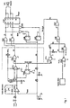
- An input signal passes the capacitor C8 and is fed to a preamplifier which contains the operational amplifier IC8B, the gain of which is regulated by the adjustable resistance network R f , and the offset level of which can be set by means of the voltage V bias which is applied to the positive input of the operational amplifier.
- the analog signal F amplified in the operational amplifier IC8B is fed to a conventional pulse width modulator which is mainly made up of the following circuit elements: constant current generator I1/capacitor C5, which forms a ramp generator, the comparator IC7B and the OR circuit IC5A.
- a system clock circuit is built up in the normal manner around a quartz crystal for the generation of a clock frequency which is relatively high in relation to the input signal, for example 32 kHz.
- This circuit generates a system clock signal A which is inverted in a buffer link, NAND circuit IC3A.
- the system clock signal A is converted by the circuit elements IC3B, the ramp reset timing circuit R8/C11/OR circuit IC2A to the ramp reset signal D, whereby the link R8/C11 determines the duration of the ramp reset pulse D.
- the ramp reset signal D sets the ramp generator I1/C5 to zero across the electric switch IC6A, so that a saw-tooth-shaped reference signal E of relatively high frequency is generated.
- This saw-tooth reference signal E is compared with the acoustically-derived signal F in the comparator IC7B, the output signal of which forms the pulse modulated output signal G.
- the pulse width modulated signal H is generated from the signal G by the OR circuit IC5A, the duty cycle of which corresponds to the amplitude of the analog input signal for a given time.
- a difference generator consisting of the OR circuit IC2C and the NAND circuit IC3C converts the pulse width modulated pulse train H to two bipolar pulse trains I and J. These pulsed drive signals must now be directly amplified and applied to a load such as a loudspeaker.
- a signal, reference clock or ref clock C is similarly derived from the system clock signal A and is delayed in relation to this through a buffer link, IC2B and IC2D, in such a way that ref clock C is timewise offset from, but otherwise occurs synchronously with, the ramp reset signal D.
- the ref clock signal C controls that the rear flank of the individual pulses in the pulse train I are practically almost coincident with a positive change C 0 in the ref clock signal C.
- the ref clock signal C controls that the leading edge of the individual pulses in the pulse train J are practically almost coincident with a positive change C 0 in the ref clock signal C.
- a power stage IC1B amplifies the signals I and J and is coupled directly to the terminals for a load which, in this example, is a loudspeaker.
- This power stage is provided with slew-rate-limiting outputs to reduce high-frequency radiation from the power stage.
- the respective pulse drive signals I and J across respective inverters IC6A and IC6B, each drive an electric switch, the outputs of which are joined in the connection K.
- the signal I drives the switch IC4B, which generates pulses with a positive reference voltage
- the signal J drives the switch IC4C which generates pulses with the voltage 0.
- Information concerning DC errors can be derived directly from the signals I and J when no signal is applied to the input of the amplifier, since the pulse length of one of the signals I or J will directly express a phase error which represents the DC error, and which depending on tolerances for the analog components easily arises, among other things due to offset errors and delays in the pulse width modulation circuit.
- the signal K is integrated across the link R3/C4, which thus forms an average value of the respective pulse trains I and J and herewith represents the DC error which has arisen in the pulse width modulator.
- the signal which is also filtered for high-frequency components by R2/C6, e.g. "glitches", is fed back to the positive input of the comparator IC8B, whereby offset is regulated to compensate for the DC error which has arisen.
- the signals are shown corresponding to a period of the signal A of around 32 ⁇ s, which corresponds to a system clock signal of 32 kHz.
- ref clock C lies at the midpoint between the flanks of a saw-tooth pulse.
- This point represents a reference point on each saw-tooth pulse.
- the point does not necessarily constitute the precise geometric midpoint between the flanks of the saw-tooth pulse, but defines a point which has the same position on each saw-tooth pulse.
- a number of signal values for the amplified and offset-regulated, analog input signal F are shown overlying the saw-tooth pulse E.
- F h represents a high signal level
- F i represents a signal level close to idling voltage
- F l represents a low signal level.
- the signal A is shown for a period corresponding to the 32 kHz system clock signal.
- the signal sequences including the formation of the signal drive pulses G, H, I and J for these three input levels are shown with the notation h, i and l below the saw-tooth pulse E in fig. 2.
- the comparator IC7B will change from high to low when the saw-tooth pulse E exceeds F h . This change defines the rear flank of the bipolar pulse drive signal Jh .
- the leading flank of the pulse drive signal J h is defined by the rising flank C 0 of ref clock C.
- the comparator IC7B changes from high to low when the saw-tooth pulse E exceeds F l .
- This change defines the leading flank of the bipolar pulse drive signal I l .
- the rear flank of the pulse drive signal I h is defined by the rising flank C 0 of ref clock C.
- the signal K represents a so-called phase error signal and is integrated for the voltage V bias which is fed back to the comparator as an offset voltage to compensate for DC errors.
- the magnitude of the V bias correction signal will depend on the length of the pulse J i or, in other words, the length of time for which the pulse J i is delayed in relation to the reference point defined by the positive flank C 0 of the ref clock C signal.
Landscapes
- Engineering & Computer Science (AREA)
- Power Engineering (AREA)
- Amplifiers (AREA)
Claims (5)
- Amplificateur de classe D pour l'amplification d'un signal d'entrée, par exemple un signal audio, comprenant un modulateur de largeur d'impulsion dans lequel un signal de référence de haute fréquence (E) est modulé en largeur d'impulsion par le signal d'entrée, un générateur de différence couplé à la sortie du modulateur de largeur d'impulsion et dans lequel sont engendrés deux signaux de commande d'impulsion bipolaires (I, J) ayant des cycles actifs qui correspondent à la grandeur du signal d'entrée à un instant donné, et un générateur d'erreur qui forme, à partir des deux signaux de commande d'impulsion, un signal correspondant à la composante de courant continu moyenne des signaux de commande d'impulsion et qui est renvoyé au modulateur de largeur d'impulsion pour l'ajustement du modulateur, de sorte que la composante de courant continu moyenne des signaux de commande d'impulsion tend vers zéro, caractérisé en ce que :le signal de référence de haute fréquence est engendré à partir d'un premier signal d'horloge (A), etle flanc avant ou le flanc arrière des impulsions individuelles dans les signaux de commande d'impulsion respectifs (I, J) sont commandés de manière à se produire en synchronisme avec un deuxième signal d'horloge (C) obtenu à partir du premier signal d'horloge (A).
- Amplificateur de classe D selon la revendication 1, caractérisé en ce que :le générateur de largeur d'impulsion comprend un générateur de dents de scie (I1, C5, IC6A) qui engendre un signal de référence de haute fréquence en dents de scie (E), et un comparateur (IC7B) dans lequel un signal régulé en décalage et amplifié (F) du signal d'entrée est comparé au signal en dents de scie (E), de sorte que le premier signal d'horloge (A) définit l'impulsion en dents de scie (E), incluant la durée de ladite impulsion en dents de scie (E), et un instant de référence (C0) défini par le deuxième signal d'horloge (C) situé entre deux flancs descendants pour une impulsion en dents de scie (E), etles impulsions individuelles dans chaque train d'impulsions respectif des signaux de commande d'impulsion (I, J) ont un flanc qui est pratiquement presque en coïncidence avec l'instant de référence précité (C0),la durée des impulsions de commande individuelles étant ainsi définie par rapport à cet instant (C0),de sorte que l'erreur de courant continu des signaux de commande d'impulsion (I, J) engendre l'ajustement du décalage pour le signal (F) amplifié à partir du signal d'entrée, par comparaison avec le signal de référence en dents de scie (E) en relation avec le retard de cet instant (C0).
- Amplificateur de classe D selon la revendication 2, caractérisé en ce que :un troisième signal d'horloge (D), qui est obtenu à partir du premier signal d'horloge (A) et qui engendre directement le signal en dents de scie (E), est légèrement décalé par rapport au signal d'horloge de référence (C), de sorte que des « déformations transitoires » qui peuvent apparaítre dans la génération du signal en dents de scie (E) n'ont pas d'influence sur la formation des signaux de commande d'impulsion (I, J) commandés par le deuxième signal d'horloge (C).
- Amplificateur de classe D selon une des revendications précédentes 2 et 3, caractérisé en ce que :un signal de sortie (G) du comparateur (IC7B), dans lequel le signal d'entrée dérivé est comparé au signal en dents de scie (E), est envoyé en outre à un premier opérateur logique numérique de base (IC5A) qui forme un signal (H), etles signaux de commande d'impulsion (I, J) sont formés à partir de ce point au moyen d'un deuxième et d'un troisième opérateurs logiques de base (IC2C, IC3C) qui fonctionnent comme des tampons et qui sont déclenchés par le deuxième signal d'horloge (C), à partir du signal de sortie (H) du premier opérateur logique de base (IC5A), d'une manière telle que les instructions individuelles dans les signaux de commande d'impulsion (I, J) ne sont jamais actives en même temps mais sont mutuellement adjacentes pendant un temps qui coïncide presque avec C0 en pratique.
- Amplificateur de classe D selon une quelconque des revendications précédentes, caractérisé en ce que :le premier signal d'horloge (A) est engendré par un générateur d'horloge construit autour d'un cristal de quartz.
Applications Claiming Priority (1)
| Application Number | Priority Date | Filing Date | Title |
|---|---|---|---|
| PCT/DK1996/000523 WO1998026501A1 (fr) | 1996-12-11 | 1996-12-11 | Amplificateur de categorie d |
Publications (2)
| Publication Number | Publication Date |
|---|---|
| EP0944956A1 EP0944956A1 (fr) | 1999-09-29 |
| EP0944956B1 true EP0944956B1 (fr) | 2003-03-26 |
Family
ID=8155870
Family Applications (1)
| Application Number | Title | Priority Date | Filing Date |
|---|---|---|---|
| EP96940647A Expired - Lifetime EP0944956B1 (fr) | 1996-12-11 | 1996-12-11 | Amplificateur classe d |
Country Status (13)
| Country | Link |
|---|---|
| US (1) | US6191650B1 (fr) |
| EP (1) | EP0944956B1 (fr) |
| JP (1) | JP3578773B2 (fr) |
| KR (1) | KR100424359B1 (fr) |
| AU (1) | AU721511B2 (fr) |
| BR (1) | BR9612811A (fr) |
| CA (1) | CA2273210C (fr) |
| DE (1) | DE69627043T2 (fr) |
| DK (1) | DK0944956T3 (fr) |
| ES (1) | ES2195026T3 (fr) |
| NO (1) | NO313479B1 (fr) |
| TW (1) | TW344913B (fr) |
| WO (1) | WO1998026501A1 (fr) |
Families Citing this family (10)
| Publication number | Priority date | Publication date | Assignee | Title |
|---|---|---|---|---|
| US6330279B1 (en) * | 1998-02-06 | 2001-12-11 | Seagate Technology Llc | System and method of correcting gain and offset error in a signal amplifier for a position sensitive detector |
| RU2153764C1 (ru) * | 1999-05-18 | 2000-07-27 | Южно-Уральский государственный университет | Развертывающий преобразователь |
| DE19929841C2 (de) * | 1999-06-29 | 2001-07-12 | Jan Quellmann | Getakteter Verstärker, insbesondere zur Verstärkung von Audiosignalen |
| EP1449404B1 (fr) * | 2001-11-30 | 2006-08-30 | Sonion A/S | Moteur a haute efficacite destine a des hauts-parleurs miniatures |
| FR2837647B1 (fr) * | 2002-03-25 | 2006-11-24 | Canon Kk | Emetteur sans fil a consommation de puissance reduite |
| EP1429455A1 (fr) * | 2002-12-11 | 2004-06-16 | Dialog Semiconductor GmbH | Linéarisation d'un amplificateur PDM de classe D |
| JP4201752B2 (ja) * | 2004-09-21 | 2008-12-24 | ローム株式会社 | オーディオパワーアンプic |
| US9239762B1 (en) * | 2009-08-11 | 2016-01-19 | Symantec Corporation | Method and apparatus for virtualizing file system placeholders at a computer |
| RU2422896C1 (ru) * | 2009-12-16 | 2011-06-27 | Государственное образовательное учреждение высшего профессионального образования "Южно-Уральский государственный университет" | Многозонный развертывающий преобразователь |
| JP2019129329A (ja) | 2018-01-22 | 2019-08-01 | 株式会社東芝 | 電力増幅器 |
Family Cites Families (8)
| Publication number | Priority date | Publication date | Assignee | Title |
|---|---|---|---|---|
| JPS5797710A (en) * | 1980-12-10 | 1982-06-17 | Toshiba Corp | Power amplifying device |
| US4689819B1 (en) | 1983-12-08 | 1996-08-13 | Knowles Electronics Inc | Class D hearing aid amplifier |
| US5014016A (en) * | 1989-04-13 | 1991-05-07 | Beltone Electronics Corporation | Switching amplifier |
| US5115206A (en) * | 1990-11-08 | 1992-05-19 | North American Philips Corp., Signetics Division | Merged differential amplifier and current source |
| US5115205A (en) * | 1990-12-28 | 1992-05-19 | Square D Company | AC amplifier with automatic DC compensation |
| US5352986A (en) | 1993-01-22 | 1994-10-04 | Digital Fidelity, Inc. | Closed loop power controller |
| US5805020A (en) * | 1996-06-27 | 1998-09-08 | Harris Corporation | Silent start class D amplifier |
| US6014055A (en) * | 1998-02-06 | 2000-01-11 | Intersil Corporation | Class D amplifier with reduced clock requirement and related methods |
-
1996
- 1996-12-11 DK DK96940647T patent/DK0944956T3/da active
- 1996-12-11 WO PCT/DK1996/000523 patent/WO1998026501A1/fr not_active Ceased
- 1996-12-11 AU AU10660/97A patent/AU721511B2/en not_active Ceased
- 1996-12-11 ES ES96940647T patent/ES2195026T3/es not_active Expired - Lifetime
- 1996-12-11 DE DE69627043T patent/DE69627043T2/de not_active Expired - Fee Related
- 1996-12-11 JP JP52593198A patent/JP3578773B2/ja not_active Expired - Fee Related
- 1996-12-11 EP EP96940647A patent/EP0944956B1/fr not_active Expired - Lifetime
- 1996-12-11 US US09/319,340 patent/US6191650B1/en not_active Expired - Lifetime
- 1996-12-11 CA CA002273210A patent/CA2273210C/fr not_active Expired - Fee Related
- 1996-12-11 KR KR10-1999-7005080A patent/KR100424359B1/ko not_active Expired - Fee Related
- 1996-12-11 BR BR9612811-9A patent/BR9612811A/pt not_active IP Right Cessation
-
1997
- 1997-09-23 TW TW086113772A patent/TW344913B/zh active
-
1999
- 1999-05-26 NO NO19992542A patent/NO313479B1/no unknown
Also Published As
| Publication number | Publication date |
|---|---|
| NO313479B1 (no) | 2002-10-07 |
| AU1066097A (en) | 1998-07-03 |
| DE69627043D1 (de) | 2003-04-30 |
| KR100424359B1 (ko) | 2004-03-24 |
| CA2273210A1 (fr) | 1998-06-18 |
| NO992542L (no) | 1999-08-03 |
| DE69627043T2 (de) | 2004-01-15 |
| TW344913B (en) | 1998-11-11 |
| NO992542D0 (no) | 1999-05-26 |
| KR20000057451A (ko) | 2000-09-15 |
| WO1998026501A8 (fr) | 2004-04-22 |
| AU721511B2 (en) | 2000-07-06 |
| JP3578773B2 (ja) | 2004-10-20 |
| CA2273210C (fr) | 2004-02-03 |
| JP2001505748A (ja) | 2001-04-24 |
| US6191650B1 (en) | 2001-02-20 |
| EP0944956A1 (fr) | 1999-09-29 |
| WO1998026501A9 (fr) | 2002-08-08 |
| WO1998026501A1 (fr) | 1998-06-18 |
| ES2195026T3 (es) | 2003-12-01 |
| DK0944956T3 (da) | 2003-05-19 |
| BR9612811A (pt) | 2000-03-14 |
Similar Documents
| Publication | Publication Date | Title |
|---|---|---|
| EP1042865B1 (fr) | Procede de commande reference par impulsion et destine a une amplification de puissance accrue d'un signal module par impulsion | |
| US7446603B2 (en) | Differential input Class D amplifier | |
| US6175272B1 (en) | Pulse—width modulation system | |
| EP1456942B1 (fr) | Amplificateur a modulation d'impulsions en duree a multiplexage a repartition dans le temps | |
| JP5253413B2 (ja) | D級電力段のためのエラー修正システム | |
| EP0944956B1 (fr) | Amplificateur classe d | |
| JP3504176B2 (ja) | 信号増幅回路 | |
| JP2003115730A (ja) | Pwm変調回路及び電力増幅回路 | |
| US7355472B2 (en) | Method and device for correcting signal distortions in an amplifier device | |
| US6771121B2 (en) | Linearization of a PDM Class-D amplifier | |
| EP1456943B1 (fr) | Commande d'attenuation pour convertisseurs de puissance numeriques | |
| JPH0431203B2 (fr) | ||
| US6320465B1 (en) | Constant duty-cycle limiting of analog input signal swing in a class-D amplifier | |
| US6163212A (en) | Power amplifier system | |
| CN1191674C (zh) | 丁类放大器 | |
| US6750705B2 (en) | Class D amplifier energy control | |
| MXPA99009025A (en) | Pulse referenced control method for enhanced power amplification of a pulse modulated signal | |
| JPH0122274Y2 (fr) |
Legal Events
| Date | Code | Title | Description |
|---|---|---|---|
| PUAI | Public reference made under article 153(3) epc to a published international application that has entered the european phase |
Free format text: ORIGINAL CODE: 0009012 |
|
| 17P | Request for examination filed |
Effective date: 19990712 |
|
| AK | Designated contracting states |
Kind code of ref document: A1 Designated state(s): BE DE DK ES FI FR GB IT NL SE |
|
| GRAG | Despatch of communication of intention to grant |
Free format text: ORIGINAL CODE: EPIDOS AGRA |
|
| 17Q | First examination report despatched |
Effective date: 20020624 |
|
| GRAG | Despatch of communication of intention to grant |
Free format text: ORIGINAL CODE: EPIDOS AGRA |
|
| GRAH | Despatch of communication of intention to grant a patent |
Free format text: ORIGINAL CODE: EPIDOS IGRA |
|
| GRAH | Despatch of communication of intention to grant a patent |
Free format text: ORIGINAL CODE: EPIDOS IGRA |
|
| GRAA | (expected) grant |
Free format text: ORIGINAL CODE: 0009210 |
|
| RIN1 | Information on inventor provided before grant (corrected) |
Inventor name: GUSTAFSSON, BOERJE Inventor name: BACKRAM, HANS-ERIK Inventor name: BACKRAM, LARS |
|
| AK | Designated contracting states |
Designated state(s): BE DE DK ES FI FR GB IT NL SE |
|
| REG | Reference to a national code |
Ref country code: GB Ref legal event code: FG4D |
|
| REF | Corresponds to: |
Ref document number: 69627043 Country of ref document: DE Date of ref document: 20030430 Kind code of ref document: P |
|
| REG | Reference to a national code |
Ref country code: DK Ref legal event code: T3 |
|
| REG | Reference to a national code |
Ref country code: SE Ref legal event code: TRGR |
|
| ET | Fr: translation filed | ||
| PLBE | No opposition filed within time limit |
Free format text: ORIGINAL CODE: 0009261 |
|
| STAA | Information on the status of an ep patent application or granted ep patent |
Free format text: STATUS: NO OPPOSITION FILED WITHIN TIME LIMIT |
|
| 26N | No opposition filed |
Effective date: 20031230 |
|
| PGFP | Annual fee paid to national office [announced via postgrant information from national office to epo] |
Ref country code: NL Payment date: 20061213 Year of fee payment: 11 |
|
| PGFP | Annual fee paid to national office [announced via postgrant information from national office to epo] |
Ref country code: ES Payment date: 20061220 Year of fee payment: 11 |
|
| PGFP | Annual fee paid to national office [announced via postgrant information from national office to epo] |
Ref country code: IT Payment date: 20061231 Year of fee payment: 11 |
|
| PGFP | Annual fee paid to national office [announced via postgrant information from national office to epo] |
Ref country code: BE Payment date: 20070115 Year of fee payment: 11 |
|
| BERE | Be: lapsed |
Owner name: *GN NETCOM A/S Effective date: 20071231 |
|
| NLV4 | Nl: lapsed or anulled due to non-payment of the annual fee |
Effective date: 20080701 |
|
| PG25 | Lapsed in a contracting state [announced via postgrant information from national office to epo] |
Ref country code: BE Free format text: LAPSE BECAUSE OF NON-PAYMENT OF DUE FEES Effective date: 20071231 |
|
| PG25 | Lapsed in a contracting state [announced via postgrant information from national office to epo] |
Ref country code: NL Free format text: LAPSE BECAUSE OF NON-PAYMENT OF DUE FEES Effective date: 20080701 |
|
| PGFP | Annual fee paid to national office [announced via postgrant information from national office to epo] |
Ref country code: DK Payment date: 20081223 Year of fee payment: 13 |
|
| PGFP | Annual fee paid to national office [announced via postgrant information from national office to epo] |
Ref country code: FI Payment date: 20081215 Year of fee payment: 13 |
|
| REG | Reference to a national code |
Ref country code: ES Ref legal event code: FD2A Effective date: 20071212 |
|
| PG25 | Lapsed in a contracting state [announced via postgrant information from national office to epo] |
Ref country code: ES Free format text: LAPSE BECAUSE OF NON-PAYMENT OF DUE FEES Effective date: 20071212 |
|
| PGFP | Annual fee paid to national office [announced via postgrant information from national office to epo] |
Ref country code: DE Payment date: 20081218 Year of fee payment: 13 |
|
| PG25 | Lapsed in a contracting state [announced via postgrant information from national office to epo] |
Ref country code: IT Free format text: LAPSE BECAUSE OF NON-PAYMENT OF DUE FEES Effective date: 20071211 |
|
| PGFP | Annual fee paid to national office [announced via postgrant information from national office to epo] |
Ref country code: FR Payment date: 20081231 Year of fee payment: 13 |
|
| REG | Reference to a national code |
Ref country code: DK Ref legal event code: EBP |
|
| PG25 | Lapsed in a contracting state [announced via postgrant information from national office to epo] |
Ref country code: FI Free format text: LAPSE BECAUSE OF NON-PAYMENT OF DUE FEES Effective date: 20091211 |
|
| REG | Reference to a national code |
Ref country code: FR Ref legal event code: ST Effective date: 20100831 |
|
| PG25 | Lapsed in a contracting state [announced via postgrant information from national office to epo] |
Ref country code: FR Free format text: LAPSE BECAUSE OF NON-PAYMENT OF DUE FEES Effective date: 20091231 |
|
| PG25 | Lapsed in a contracting state [announced via postgrant information from national office to epo] |
Ref country code: DE Free format text: LAPSE BECAUSE OF NON-PAYMENT OF DUE FEES Effective date: 20100701 |
|
| PG25 | Lapsed in a contracting state [announced via postgrant information from national office to epo] |
Ref country code: DK Free format text: LAPSE BECAUSE OF NON-PAYMENT OF DUE FEES Effective date: 20100104 |
|
| PGFP | Annual fee paid to national office [announced via postgrant information from national office to epo] |
Ref country code: SE Payment date: 20121221 Year of fee payment: 17 |
|
| REG | Reference to a national code |
Ref country code: SE Ref legal event code: EUG |
|
| PG25 | Lapsed in a contracting state [announced via postgrant information from national office to epo] |
Ref country code: SE Free format text: LAPSE BECAUSE OF NON-PAYMENT OF DUE FEES Effective date: 20131212 |
|
| PGFP | Annual fee paid to national office [announced via postgrant information from national office to epo] |
Ref country code: GB Payment date: 20141229 Year of fee payment: 19 |
|
| GBPC | Gb: european patent ceased through non-payment of renewal fee |
Effective date: 20151211 |
|
| PG25 | Lapsed in a contracting state [announced via postgrant information from national office to epo] |
Ref country code: GB Free format text: LAPSE BECAUSE OF NON-PAYMENT OF DUE FEES Effective date: 20151211 |