EP0945215A2 - Substrat céramique et son procédé de polissage - Google Patents
Substrat céramique et son procédé de polissage Download PDFInfo
- Publication number
- EP0945215A2 EP0945215A2 EP99302250A EP99302250A EP0945215A2 EP 0945215 A2 EP0945215 A2 EP 0945215A2 EP 99302250 A EP99302250 A EP 99302250A EP 99302250 A EP99302250 A EP 99302250A EP 0945215 A2 EP0945215 A2 EP 0945215A2
- Authority
- EP
- European Patent Office
- Prior art keywords
- polishing
- ceramic substrate
- substrate
- ceramic
- polished
- Prior art date
- Legal status (The legal status is an assumption and is not a legal conclusion. Google has not performed a legal analysis and makes no representation as to the accuracy of the status listed.)
- Granted
Links
- 239000000758 substrate Substances 0.000 title claims abstract description 124
- 239000000919 ceramic Substances 0.000 title claims abstract description 98
- 238000005498 polishing Methods 0.000 title claims abstract description 91
- 238000000034 method Methods 0.000 title claims abstract description 25
- 239000006061 abrasive grain Substances 0.000 claims abstract description 31
- 238000007517 polishing process Methods 0.000 claims abstract description 11
- PMHQVHHXPFUNSP-UHFFFAOYSA-M copper(1+);methylsulfanylmethane;bromide Chemical compound Br[Cu].CSC PMHQVHHXPFUNSP-UHFFFAOYSA-M 0.000 claims description 14
- 230000003746 surface roughness Effects 0.000 description 24
- PNEYBMLMFCGWSK-UHFFFAOYSA-N aluminium oxide Inorganic materials [O-2].[O-2].[O-2].[Al+3].[Al+3] PNEYBMLMFCGWSK-UHFFFAOYSA-N 0.000 description 23
- 239000000463 material Substances 0.000 description 17
- 229910052581 Si3N4 Inorganic materials 0.000 description 13
- 229910052593 corundum Inorganic materials 0.000 description 13
- 229910001845 yogo sapphire Inorganic materials 0.000 description 13
- 235000019592 roughness Nutrition 0.000 description 11
- 229910010293 ceramic material Inorganic materials 0.000 description 9
- 239000011347 resin Substances 0.000 description 9
- 229920005989 resin Polymers 0.000 description 9
- 238000000227 grinding Methods 0.000 description 7
- IJGRMHOSHXDMSA-UHFFFAOYSA-N Atomic nitrogen Chemical compound N#N IJGRMHOSHXDMSA-UHFFFAOYSA-N 0.000 description 4
- 238000005245 sintering Methods 0.000 description 4
- 239000004677 Nylon Substances 0.000 description 3
- 239000012298 atmosphere Substances 0.000 description 3
- 239000004745 nonwoven fabric Substances 0.000 description 3
- 229920001778 nylon Polymers 0.000 description 3
- 239000000843 powder Substances 0.000 description 3
- 238000012360 testing method Methods 0.000 description 3
- VYPSYNLAJGMNEJ-UHFFFAOYSA-N Silicium dioxide Chemical compound O=[Si]=O VYPSYNLAJGMNEJ-UHFFFAOYSA-N 0.000 description 2
- 238000007796 conventional method Methods 0.000 description 2
- 238000009499 grossing Methods 0.000 description 2
- 238000010438 heat treatment Methods 0.000 description 2
- 238000001513 hot isostatic pressing Methods 0.000 description 2
- 229910052757 nitrogen Inorganic materials 0.000 description 2
- 230000009467 reduction Effects 0.000 description 2
- 238000007650 screen-printing Methods 0.000 description 2
- HBMJWWWQQXIZIP-UHFFFAOYSA-N silicon carbide Chemical compound [Si+]#[C-] HBMJWWWQQXIZIP-UHFFFAOYSA-N 0.000 description 2
- 229910010271 silicon carbide Inorganic materials 0.000 description 2
- HQVNEWCFYHHQES-UHFFFAOYSA-N silicon nitride Chemical compound N12[Si]34N5[Si]62N3[Si]51N64 HQVNEWCFYHHQES-UHFFFAOYSA-N 0.000 description 2
- 239000002002 slurry Substances 0.000 description 2
- 229910017083 AlN Inorganic materials 0.000 description 1
- OKTJSMMVPCPJKN-UHFFFAOYSA-N Carbon Chemical compound [C] OKTJSMMVPCPJKN-UHFFFAOYSA-N 0.000 description 1
- 238000005452 bending Methods 0.000 description 1
- 239000011230 binding agent Substances 0.000 description 1
- 229910052799 carbon Inorganic materials 0.000 description 1
- 230000008859 change Effects 0.000 description 1
- 229910052681 coesite Inorganic materials 0.000 description 1
- 238000005336 cracking Methods 0.000 description 1
- 229910052906 cristobalite Inorganic materials 0.000 description 1
- 238000005238 degreasing Methods 0.000 description 1
- 229910003460 diamond Inorganic materials 0.000 description 1
- 239000010432 diamond Substances 0.000 description 1
- 238000009826 distribution Methods 0.000 description 1
- 238000007606 doctor blade method Methods 0.000 description 1
- 229920001971 elastomer Polymers 0.000 description 1
- 229920001821 foam rubber Polymers 0.000 description 1
- 239000011521 glass Substances 0.000 description 1
- 230000001771 impaired effect Effects 0.000 description 1
- 238000004519 manufacturing process Methods 0.000 description 1
- 239000012299 nitrogen atmosphere Substances 0.000 description 1
- 239000003960 organic solvent Substances 0.000 description 1
- 230000001590 oxidative effect Effects 0.000 description 1
- 239000004033 plastic Substances 0.000 description 1
- 239000002984 plastic foam Substances 0.000 description 1
- 238000013001 point bending Methods 0.000 description 1
- 230000002035 prolonged effect Effects 0.000 description 1
- 239000000377 silicon dioxide Substances 0.000 description 1
- 229910052682 stishovite Inorganic materials 0.000 description 1
- 239000004575 stone Substances 0.000 description 1
- 229910052905 tridymite Inorganic materials 0.000 description 1
- XLYOFNOQVPJJNP-UHFFFAOYSA-N water Substances O XLYOFNOQVPJJNP-UHFFFAOYSA-N 0.000 description 1
- 239000002759 woven fabric Substances 0.000 description 1
Images




Classifications
-
- B—PERFORMING OPERATIONS; TRANSPORTING
- B24—GRINDING; POLISHING
- B24B—MACHINES, DEVICES, OR PROCESSES FOR GRINDING OR POLISHING; DRESSING OR CONDITIONING OF ABRADING SURFACES; FEEDING OF GRINDING, POLISHING, OR LAPPING AGENTS
- B24B5/00—Machines or devices designed for grinding surfaces of revolution on work, including those which also grind adjacent plane surfaces; Accessories therefor
- B24B5/18—Machines or devices designed for grinding surfaces of revolution on work, including those which also grind adjacent plane surfaces; Accessories therefor involving centreless means for supporting, guiding, floating or rotating work
- B24B5/20—Machines or devices designed for grinding surfaces of revolution on work, including those which also grind adjacent plane surfaces; Accessories therefor involving centreless means for supporting, guiding, floating or rotating work involving grooved abrading blocks
-
- B—PERFORMING OPERATIONS; TRANSPORTING
- B24—GRINDING; POLISHING
- B24B—MACHINES, DEVICES, OR PROCESSES FOR GRINDING OR POLISHING; DRESSING OR CONDITIONING OF ABRADING SURFACES; FEEDING OF GRINDING, POLISHING, OR LAPPING AGENTS
- B24B29/00—Machines or devices for polishing surfaces on work by means of tools made of soft or flexible material with or without the application of solid or liquid polishing agents
-
- B—PERFORMING OPERATIONS; TRANSPORTING
- B24—GRINDING; POLISHING
- B24B—MACHINES, DEVICES, OR PROCESSES FOR GRINDING OR POLISHING; DRESSING OR CONDITIONING OF ABRADING SURFACES; FEEDING OF GRINDING, POLISHING, OR LAPPING AGENTS
- B24B7/00—Machines or devices designed for grinding plane surfaces on work, including polishing plane glass surfaces; Accessories therefor
- B24B7/20—Machines or devices designed for grinding plane surfaces on work, including polishing plane glass surfaces; Accessories therefor characterised by a special design with respect to properties of the material of non-metallic articles to be ground
- B24B7/22—Machines or devices designed for grinding plane surfaces on work, including polishing plane glass surfaces; Accessories therefor characterised by a special design with respect to properties of the material of non-metallic articles to be ground for grinding inorganic material, e.g. stone, ceramics, porcelain
-
- G—PHYSICS
- G03—PHOTOGRAPHY; CINEMATOGRAPHY; ANALOGOUS TECHNIQUES USING WAVES OTHER THAN OPTICAL WAVES; ELECTROGRAPHY; HOLOGRAPHY
- G03G—ELECTROGRAPHY; ELECTROPHOTOGRAPHY; MAGNETOGRAPHY
- G03G15/00—Apparatus for electrographic processes using a charge pattern
- G03G15/20—Apparatus for electrographic processes using a charge pattern for fixing, e.g. by using heat
- G03G15/2003—Apparatus for electrographic processes using a charge pattern for fixing, e.g. by using heat using heat
- G03G15/2014—Apparatus for electrographic processes using a charge pattern for fixing, e.g. by using heat using heat using contact heat
- G03G15/2053—Structural details of heat elements, e.g. structure of roller or belt, eddy current, induction heating
-
- Y—GENERAL TAGGING OF NEW TECHNOLOGICAL DEVELOPMENTS; GENERAL TAGGING OF CROSS-SECTIONAL TECHNOLOGIES SPANNING OVER SEVERAL SECTIONS OF THE IPC; TECHNICAL SUBJECTS COVERED BY FORMER USPC CROSS-REFERENCE ART COLLECTIONS [XRACs] AND DIGESTS
- Y10—TECHNICAL SUBJECTS COVERED BY FORMER USPC
- Y10T—TECHNICAL SUBJECTS COVERED BY FORMER US CLASSIFICATION
- Y10T428/00—Stock material or miscellaneous articles
- Y10T428/24—Structurally defined web or sheet [e.g., overall dimension, etc.]
- Y10T428/24355—Continuous and nonuniform or irregular surface on layer or component [e.g., roofing, etc.]
-
- Y—GENERAL TAGGING OF NEW TECHNOLOGICAL DEVELOPMENTS; GENERAL TAGGING OF CROSS-SECTIONAL TECHNOLOGIES SPANNING OVER SEVERAL SECTIONS OF THE IPC; TECHNICAL SUBJECTS COVERED BY FORMER USPC CROSS-REFERENCE ART COLLECTIONS [XRACs] AND DIGESTS
- Y10—TECHNICAL SUBJECTS COVERED BY FORMER USPC
- Y10T—TECHNICAL SUBJECTS COVERED BY FORMER US CLASSIFICATION
- Y10T428/00—Stock material or miscellaneous articles
- Y10T428/24—Structurally defined web or sheet [e.g., overall dimension, etc.]
- Y10T428/24355—Continuous and nonuniform or irregular surface on layer or component [e.g., roofing, etc.]
- Y10T428/24372—Particulate matter
- Y10T428/24413—Metal or metal compound
-
- Y—GENERAL TAGGING OF NEW TECHNOLOGICAL DEVELOPMENTS; GENERAL TAGGING OF CROSS-SECTIONAL TECHNOLOGIES SPANNING OVER SEVERAL SECTIONS OF THE IPC; TECHNICAL SUBJECTS COVERED BY FORMER USPC CROSS-REFERENCE ART COLLECTIONS [XRACs] AND DIGESTS
- Y10—TECHNICAL SUBJECTS COVERED BY FORMER USPC
- Y10T—TECHNICAL SUBJECTS COVERED BY FORMER US CLASSIFICATION
- Y10T428/00—Stock material or miscellaneous articles
- Y10T428/24—Structurally defined web or sheet [e.g., overall dimension, etc.]
- Y10T428/24942—Structurally defined web or sheet [e.g., overall dimension, etc.] including components having same physical characteristic in differing degree
- Y10T428/2495—Thickness [relative or absolute]
-
- Y—GENERAL TAGGING OF NEW TECHNOLOGICAL DEVELOPMENTS; GENERAL TAGGING OF CROSS-SECTIONAL TECHNOLOGIES SPANNING OVER SEVERAL SECTIONS OF THE IPC; TECHNICAL SUBJECTS COVERED BY FORMER USPC CROSS-REFERENCE ART COLLECTIONS [XRACs] AND DIGESTS
- Y10—TECHNICAL SUBJECTS COVERED BY FORMER USPC
- Y10T—TECHNICAL SUBJECTS COVERED BY FORMER US CLASSIFICATION
- Y10T428/00—Stock material or miscellaneous articles
- Y10T428/24—Structurally defined web or sheet [e.g., overall dimension, etc.]
- Y10T428/24942—Structurally defined web or sheet [e.g., overall dimension, etc.] including components having same physical characteristic in differing degree
- Y10T428/2495—Thickness [relative or absolute]
- Y10T428/24967—Absolute thicknesses specified
-
- Y—GENERAL TAGGING OF NEW TECHNOLOGICAL DEVELOPMENTS; GENERAL TAGGING OF CROSS-SECTIONAL TECHNOLOGIES SPANNING OVER SEVERAL SECTIONS OF THE IPC; TECHNICAL SUBJECTS COVERED BY FORMER USPC CROSS-REFERENCE ART COLLECTIONS [XRACs] AND DIGESTS
- Y10—TECHNICAL SUBJECTS COVERED BY FORMER USPC
- Y10T—TECHNICAL SUBJECTS COVERED BY FORMER US CLASSIFICATION
- Y10T428/00—Stock material or miscellaneous articles
- Y10T428/26—Web or sheet containing structurally defined element or component, the element or component having a specified physical dimension
-
- Y—GENERAL TAGGING OF NEW TECHNOLOGICAL DEVELOPMENTS; GENERAL TAGGING OF CROSS-SECTIONAL TECHNOLOGIES SPANNING OVER SEVERAL SECTIONS OF THE IPC; TECHNICAL SUBJECTS COVERED BY FORMER USPC CROSS-REFERENCE ART COLLECTIONS [XRACs] AND DIGESTS
- Y10—TECHNICAL SUBJECTS COVERED BY FORMER USPC
- Y10T—TECHNICAL SUBJECTS COVERED BY FORMER US CLASSIFICATION
- Y10T428/00—Stock material or miscellaneous articles
- Y10T428/26—Web or sheet containing structurally defined element or component, the element or component having a specified physical dimension
- Y10T428/266—Web or sheet containing structurally defined element or component, the element or component having a specified physical dimension of base or substrate
-
- Y—GENERAL TAGGING OF NEW TECHNOLOGICAL DEVELOPMENTS; GENERAL TAGGING OF CROSS-SECTIONAL TECHNOLOGIES SPANNING OVER SEVERAL SECTIONS OF THE IPC; TECHNICAL SUBJECTS COVERED BY FORMER USPC CROSS-REFERENCE ART COLLECTIONS [XRACs] AND DIGESTS
- Y10—TECHNICAL SUBJECTS COVERED BY FORMER USPC
- Y10T—TECHNICAL SUBJECTS COVERED BY FORMER US CLASSIFICATION
- Y10T428/00—Stock material or miscellaneous articles
- Y10T428/26—Web or sheet containing structurally defined element or component, the element or component having a specified physical dimension
- Y10T428/268—Monolayer with structurally defined element
Definitions
- the present invention relates to ceramic substrates having a polished surface with high surface smoothness and methods of polishing such ceramic substrates, and more particularly, to a ceramic substrate for use in a thermal fixation device for toner image such as a copying machine and a printer and a method of polishing such a ceramic substrate.
- the surface of the ceramic material should be polished or ground into smoothness.
- various proposed methods of smoothing a ceramic surface depending upon the shape, use, required smoothness and the like of the ceramic material.
- One typical method of polishing a ceramic material is barrel-polishing, according to which a ceramic material and an abrasive are put together into a container to polish the ceramic material by rotation or vibration, and Japanese Patent Laying-Open No. 58-192745 for example discloses a method of polishing a ceramic element by a vibrating barrel using a pier-shaped abrasive.
- Other methods of treating a ceramic surface include lapping, honing, and grinding. These methods employ hone or abrasive grains to pressurize the ceramic material to be treated and the surface is ground.
- the conventional, typical methods of polishing or grinding described above are suitable for treating relatively small and thick ceramic elements, but are not appropriate for smoothing the surface of a ceramic substrate having a large area and a relatively small thickness such as a substrate for a ceramic heater in a thermal fixation device for toner image.
- a thin ceramic substrate is sometimes destroyed by a grinder during rotation or vibration.
- a ceramic substrate is prone to cracking, because a prescribed pressure is applied between abrasive grains or a grinder used and the ceramic material.
- the lapping, honing, grinding or the like requests that the untreated surface must be ground as much as 0.1 to 0.2mm in order to eliminate variations in the surface smoothness by the working. Therefore, a ceramic substrate having a thickness larger than a finished product by the margin for working should be prepared, which increases the material cost.
- the present invention is directed to a solution to the problem, and it is an object of the present invention to provide a ceramic substrate having a large area, a relatively small thickness and a smooth surface such as a ceramic substrate for use in a ceramic heater in a thermal fixation device for toner image and to provide a method of polishing the surface of such a ceramic substrate having a large area and a relatively small thickness into smoothness without damaging the surface.
- a method of polishing a ceramic substrate according to the present invention uses a ductile rotating body containing abrasive grains, and the surface of the ceramic substrate is polished by the circumferential portion of the rotating body.
- This polishing method is preferable for polishing a thin ceramic substrate, particularly, a ceramic substrate as thin as 2.0mm or less.
- the direction orthogonal to the rotating axis of the rotating body is preferably inclined by an angle in the range from 10° to 80° relative to the direction of polishing the ceramic substrate. If this angle is smaller than 10° or larger than 80°, a line is impressed on the ceramic substrate by the abrasive grains, and the surface roughness is relatively increased.
- the polishing process may be divided into two or more steps and the average grain size of abrasive grains contained in the rotating body may be reduced stepwise.
- a ceramic substrate resulting from the polishing as described above has at least one surface polished, which surface is formed by a substantially flat portion and a recessed portion remaining in the flat portion.
- Such a ceramic substrate is suitable for a ceramic substrate having a large area and a relatively small thickness such as a substrate for a ceramic heater used in a thermal fixation device for toner image.
- the flat portion herein includes microscopically small irregularities.
- the surface of a ceramic substrate is polished using the circumferential portion of a columnar- or disc-shaped, ductile rotating body containing abrasive grains.
- the rotating body has only to be able to hold abrasive grains and be ductile, and woven or nonwoven fabric, plastic foam (foamed plastic or sponge), rubber foam (rubber sponge) or the like is preferable.
- plastic foam fuoamed plastic or sponge
- rubber foam rubber sponge
- the abrasive grains contained in the rotating body may be conventional abrasive grains such as alumina and silicon carbide.
- recessed portions 10a and raised portions 10b as shown in Fig. 1 on the surface of a ceramic substrate formed of a sintered body, and the amplitude of the maximum irregularities is sometimes over 10 ⁇ m.
- the surface roughness curve of a sintered body having a center line average height Ra of 0.78 ⁇ m before polishing based on the Japanese Industrial Standard (JIS R 1600) and a maximum height Rmax of 9.7 ⁇ m based on the standard is shown in Fig. 6.
- the resulting polished surface microscopically includes substantially flat portions 10c and recessed portions 10a remaining between flat portions 10c, so that a relatively smooth polished surface with a small irregularity amplitude can result for a smaller amount of polishing.
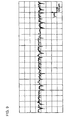
- Fig. 7 is a surface roughness curve resulting after polishing a aluminum nitride sintered body having a surface roughness shown in Fig. 6 using a rotating body containing abrasive grains of alumina (Al 2 O 3 )-based ceramic which passes a #320 mesh screen (hereinafter "#320 mesh-pass) by a method according to the present invention.
- center line average height Ra is 0.34 ⁇ m and maximum height Rmax is 5.4 ⁇ m.
- #320 mesh refers to a mesh having 320 openings per linear inch.
- the size of the actual mesh is obtained by subtracting the wire size forming the mesh from the value obtained by dividing one inch by 320. This also applies to #80 mesh, #150 mesh, #600 mesh, and #1000 mesh in the following description.
- the conventional barrel-polishing mainly removes raised portions but removes recessed portions as well, and the raised and recessed portions are generally rounded off in polishing.
- Lapping, honing and grinding trim the entire surface regardless of the surface irregularities, and the resulting polished surface has impressions caused by hard abrasive grains or the like, a large number of recessed and raised portions of a small amplitude remain microscopically.
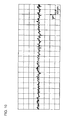
- the roughness curves of a barrel-polished product and a lapped product are given in Figs. 8 and 9 as examples of such a polished surface.
- the roughness curve in Fig. 8 corresponds to a surface resulting by barrel-polishing the surface of an aluminum nitride sintered body in Fig. 6 by a #320-GC (Green Carbon) barrel stone
- the roughness curve in Fig. 9 corresponds to a surface resulting from lapping using a GC hone having a similar roughness.
- a ceramic substrate is in point-contact with a hone or abrasive grains, a large pressure is locally applied upon the ceramic substrate. If the loaded pressure is too large, the shoulder of a corner portion of the ceramic substrate is prone to be broken, rounded off, or chip. A relatively thin substrate could be cracked, in other words, the local concentration of pressure could damage the substrate. In a normal grinding, the substrate is ground as much as 0.1 to 0.2mm thickness-wise in order to avoid variations in grinding, a very large material loss is inevitable.
- the rotating body used according to the present invention is ductile and easily deforms when it is pressed against a ceramic substrate to be in plane-contact with the ceramic surface.
- the pressure upon the surface being polished is dispersed within each part of the ceramic substrate, which prevents the local concentration of pressure, and the ceramic substrate will be hardly damaged.
- the pressure can be dispersed relatively evenly within a wide range of the surface being polished, a corner portion of the substrate will not be broken or rounded off, deformation such as cracks and chipping at the portion can be prevented and cracks in the substrate itself can be prevented so that the method is preferable for polishing a thin ceramic substrate, particularly a substrate having a thickness equal to or smaller than 2.0mm.
- the deformation of the rotating body and even distribution of abrasive grains reduce variations in the polishing and almost no material loss is caused.
- the polishing process is divided into a number of steps, and the average grain size of abrasive grains contained in the rotating body is reduced stepwise, and therefore the surface roughness of the resulting polished surface can be even further reduced. More specifically, the surface is polished first using a rotating body containing abrasive grains having a large average grain size. Since the average grain size is large, the polishing force is large accordingly, and large raised portions present on the surface are removed. Subsequently, rotating bodies each containing abrasive grains having an average grain size smaller than the previous polishing step are used for repeating the polishing.
- the gain size of abrasive grains contained in the rotating body is set as #80 mesh-pass first, then #150 mesh-pass next, followed by #320 mesh-pass sequentially, so that small raised portions which cannot removed in a polishing step can be removed in the following steps.
- Fig. 10 shows the roughness curve of a surface formed by polishing the surface of an aluminum nitride sintered body having the surface state shown in Fig. 6 in the multiple steps, and center line average height Ra is 0.16 ⁇ m and Rmax is 1.5 ⁇ m.
- polishing is preferably performed such that the direction (rotating direction) D 1 orthogonal to the rotating axis of rotating body 11 is inclined relative to the polishing direction D 0 of ceramic substrate 10. If polishing direction D 0 and rotating direction D 1 are the same, impressions caused by abrasive grains are formed linearly on ceramic substrate 10, the surface roughness is relatively increased. Meanwhile, if prescribed angle ⁇ is formed between polishing direction D 0 and rotating direction D 1 , linear impressions will not be formed, and a smoother polished surface results. Angle ⁇ is preferably in the range from 10° to 80° and more preferably in the range from 30° to 60°.
- the polished surface of a ceramic substrate obtained by the above described polishing method according to the present invention includes flat portions and recessed portions therebetween.
- the flat portions have an average width in the range from several ⁇ m to 50 ⁇ m microscopically, and preferably includes ups and downs (fine irregularities) equal to or smaller than 0.2 ⁇ m raised toward the surface.
- the ceramic substrate to be polished is not particularly limited and may be an alumina, aluminum nitride, silicon nitride substrate or the like. Since the aluminum nitride substrate is generally formed by grains as large as several ⁇ m, grains often drop out by stress applied in a polishing operation, and this is why it is difficult to obtain a smooth surface by a conventional method, but the pressure against the surface being polished is dispersed according to the present invention, which prevents the drop out of grains caused by the concentration of the pressure, so that an even smoother polished surface results.
- the polished surface formed by the polishing method according to the present invention includes substantially flat portions and recessed portions therebetween, the height of microscopical raised portions on the flat portions is small, a relatively smooth surface with a small irregularity amplitude results, and therefore when the surface is used as a sliding surface sliding on another material and/or object, a preferable sliding characteristic results. Furthermore, by positioning the ceramic substrate such that the rotation or moving direction of a workpiece is aligned or approximated to the (constant) rotation direction of the rotating body in a polishing operation, the friction resistance with the workpiece can be reduced, which allows for a higher sliding characteristic.
- the sliding characteristic of a ceramic substrate according to the present invention is particularly advantageous when a workpiece to slide on is softer than the ceramic substrate, because the substantially flat portions having a small raised portion are in contact with the workpiece while sliding so that the friction resistance is small and the attacking force on the workpiece is small.
- the ceramic substrate according to the present invention is particularly advantageously used for the substrate for the ceramic heater.
- the recessed portion of the polished surface is preferably reduced as much as possible in order to improve the sliding characteristic. To this end, however, time required for polishing is prolonged, which impedes the productivity and therefore the time required for polishing must be set not to impede the productivity.
- a resin support body 2 is attached with a ceramic heater 1
- a heat-resisting resin film 3 is rotatably provided at the outer circumferential portion of support body 2
- a pressurizing roller 4 is disposed opposite to ceramic heater 1 with heat-resisting resin film 3 therebetween.
- a transfer material 5 having an unfixed toner image 6a is transferred at a prescribed speed between pressurizing roller 4 and heat-resisting resin film 3, pressurized by pressurizing roller 4 and heated by ceramic heater 1, so that toner image 6b is fixed on transfer material 5.
- Ceramic powder materials Al 2 O 3 , AlN and Si 3 N 4 were each added with a sintering aid, then an organic solvent and a binder, and mixed by a ball mill to obtain their slurries.
- the resultant slurries were each formed into a sheet by a doctor blade method and cut into a prescribed shape, followed by degreasing in a nitrogen atmosphere at 900°C. Then, these ceramic materials were sintered in a non-oxidizing atmosphere at optimum temperatures for them and formed into ceramic substrates.
- reduction in the thickness of the ceramic substrate according to the present invention is from 4 ⁇ m to 6 ⁇ m at most, in other words, there was little material loss, while the material loss was great according to the conventional methods, particularly according to the lapping.
- an AlN substrate according to the first embodiment improvements in the surface roughness by multi-step polishing were observed. More specifically, in each of the steps, alumina abrasive grains were contained in a rotating body of nylon nonwoven fabric having a diameter of 300mm, and polishing was performed at a rotating speed of 1000 rev/min. In the multi-step polishing, a rotating body containing #150 mesh-pass was used first, then the grain size of abrasive grains was reduced stepwise to #320 mesh-pass, then to #600 mesh-pass and then to #1000 mesh-pass. Center line average height Ra was measured as the surface roughness of a substrate obtained in each step, and the result is given in the following Table 3.
- an AlN substrate was polished by rotating bodies containing #320 mesh-pass, #600 mesh-pass and #1000 mesh-pass alumina grains, and then again polished using rotating bodies containing alumina grains of larger sizes, in other words, 150# mesh-pass, #320 mesh-pass and #600 mesh-pass alumina abrasive grains.
- the center line average height Ra of each of the resulting substrates was measured as the surface roughness, and the result is given as the surface roughness Ra after the polishing in the following Table 3.
- polishing was performed at different angles ⁇ between the advancing direction of the AlN substrate (the polishing direction) and the rotating direction of the rotating body, and the influence of angle ⁇ upon the surface roughness of the resulting polished surface was observed.
- the polishing conditions were the same as those of the first embodiment except that the rotating body used contained #150 mesh-pass alumina abrasive grains.
- Angle ⁇ (°) Surface roughness before polishing Ra ( ⁇ m)
- Surface roughness after polishing Ra ( ⁇ m) 0 0.90 0.30 5 0.90 0.29 10 0.90 0.24 30 0.90 0.18 45 0.90 0.16 60 0.90 0.17 80 0.90 0.25 90 0.90 0.32
- changing angle ⁇ formed between the rotating direction of the rotating body and the polishing direction of the substrate changes the surface roughness, and the surface roughness Ra of the AIN substrate after polishing is significantly reduced when angle ⁇ is in the range from 10° to 80°, more preferably in the range from 30° to 60° than when the angle is 0° (in parallel) and 90° (at right angles).
- an AlN substrate having a length of 300mm, a width of 10mm and a thickness of 1.0mm and an AlN substrate having a length of 100mm, a width of 300mm and a thickness of 1.3mm were manufactured.
- the following polishing operations were performed to these AlN substrates.
- the AlN substrate as thick as 1.0mm was wet-polished using a nylon sponge rotating body containing SiC abrasive grains having a diameter of 400mm at a rotating speed of 800 rev/min while applying water to the rotating body. More specifically, angle ⁇ formed between the rotating direction and the polishing direction was 30°, and the grain size of abrasive grains was changed from #150 mesh-pass, to #320, #600 and to #1000 mesh-pass stepwise for multi-step polishing.
- the AIN substrate as thick as 1.3mm was polished to 1.0mm by lapping and cut into a piece of 300mm ⁇ 10mm.
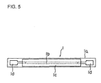
- Each of the AlN substrates after polishing was used to manufacture a ceramic heater 1 used in a thermal fixation device for toner image as shown in Fig. 5. More specifically, a heating element 1b was formed by Ag-Pd paste by screen printing and an electrode 1d was formed by Ag paste at the polishing surface of each ceramic substrate la, followed by baking in atmosphere at 880°C. Then, glass paste was applied onto heating element 1b by screen printing, followed by baking at 700°C in atmosphere to form a protection film 1c.
- Ceramic heaters 1 thus obtained were each attached to a thermal fixation device for toner image as shown in Fig. 4 and its durability was tested.
- the temperature of ceramic heater 1c was set to 180°C
- the rotation number of pressurizing roller 4 and heat-resisting resin film 3 was set to 40 rev/min.
- the heat-resisting resin film stopped rotating after 150 hours since the start of the durability test. Observing the sliding surface between the heat-resisting resin film and the heater revealed that departed AlN grains were present which probably impaired the sliding ability and stopped the rotation of the heat-resisting film.
- a ceramic substrate having a small thickness and a large area can be easily and inexpensively polished without damages such as cracks to produce a polished surface having high smoothness.
- the invention is particularly suitable for polishing an aluminum nitride substrate, grains of which easily depart.
- An aluminum nitride substrate polished according to the present invention is particularly preferably used as a substrate for a ceramic heater in a thermal fixation device for toner image.
Landscapes
- Engineering & Computer Science (AREA)
- Mechanical Engineering (AREA)
- Physics & Mathematics (AREA)
- General Physics & Mathematics (AREA)
- Chemical & Material Sciences (AREA)
- Ceramic Engineering (AREA)
- Inorganic Chemistry (AREA)
- Ceramic Products (AREA)
- Finish Polishing, Edge Sharpening, And Grinding By Specific Grinding Devices (AREA)
- Grinding Of Cylindrical And Plane Surfaces (AREA)
- Fixing For Electrophotography (AREA)
- Compositions Of Oxide Ceramics (AREA)
Applications Claiming Priority (4)
| Application Number | Priority Date | Filing Date | Title |
|---|---|---|---|
| JP7520898 | 1998-03-24 | ||
| JP7520898 | 1998-03-24 | ||
| JP1972799 | 1999-01-28 | ||
| JP11019727A JPH11335158A (ja) | 1998-03-24 | 1999-01-28 | セラミックス基板及びその研磨方法 |
Publications (3)
| Publication Number | Publication Date |
|---|---|
| EP0945215A2 true EP0945215A2 (fr) | 1999-09-29 |
| EP0945215A3 EP0945215A3 (fr) | 2002-08-21 |
| EP0945215B1 EP0945215B1 (fr) | 2004-06-09 |
Family
ID=26356577
Family Applications (1)
| Application Number | Title | Priority Date | Filing Date |
|---|---|---|---|
| EP99302250A Expired - Lifetime EP0945215B1 (fr) | 1998-03-24 | 1999-03-23 | Substrat céramique et son procédé de polissage |
Country Status (6)
| Country | Link |
|---|---|
| US (2) | US6458444B1 (fr) |
| EP (1) | EP0945215B1 (fr) |
| JP (1) | JPH11335158A (fr) |
| KR (1) | KR100334597B1 (fr) |
| CA (1) | CA2266145C (fr) |
| DE (1) | DE69917826T2 (fr) |
Families Citing this family (14)
| Publication number | Priority date | Publication date | Assignee | Title |
|---|---|---|---|---|
| WO2000069219A1 (fr) * | 1999-05-07 | 2000-11-16 | Ibiden Co., Ltd. | Plaque chauffante et son procede de fabrication |
| JP4559574B2 (ja) * | 1999-12-27 | 2010-10-06 | 株式会社東芝 | 回路基板用セラミックス基板および回路基板 |
| WO2001066488A1 (fr) * | 2000-03-07 | 2001-09-13 | Ibiden Co., Ltd. | Substrat ceramique pour fabrication/inspection de semi-conducteur |
| US6787706B2 (en) | 2001-02-21 | 2004-09-07 | Kyocera Corporation | Ceramic circuit board |
| JP2002313890A (ja) | 2001-04-11 | 2002-10-25 | Sumitomo Electric Ind Ltd | 被加熱物搭載用ヒータ部材およびそれを用いた基板処理装置 |
| JP2003201148A (ja) * | 2001-10-31 | 2003-07-15 | Nippon Sheet Glass Co Ltd | 情報記録媒体用ガラス基板の化学強化用ホルダー |
| US6811467B1 (en) | 2002-09-09 | 2004-11-02 | Seagate Technology Llc | Methods and apparatus for polishing glass substrates |
| US8597743B2 (en) | 2005-08-11 | 2013-12-03 | Tokuyama Corporation | Aluminum nitride sintered body |
| JP2007053209A (ja) * | 2005-08-17 | 2007-03-01 | Tdk Corp | セラミック電子部品の製造方法 |
| JP4777291B2 (ja) * | 2006-04-28 | 2011-09-21 | シャープ株式会社 | 画像形成装置およびそれに用いられるプロセスカートリッジ |
| US8580593B2 (en) * | 2009-09-10 | 2013-11-12 | Micron Technology, Inc. | Epitaxial formation structures and associated methods of manufacturing solid state lighting devices |
| FR2992313B1 (fr) * | 2012-06-21 | 2014-11-07 | Eurokera | Article vitroceramique et procede de fabrication |
| JP6397592B1 (ja) * | 2017-10-02 | 2018-09-26 | 住友化学株式会社 | スパッタリングターゲットの製造方法およびスパッタリングターゲット |
| JP7637711B2 (ja) * | 2023-03-16 | 2025-02-28 | 株式会社Maruwa | 窒化ケイ素板及びその製造方法 |
Family Cites Families (17)
| Publication number | Priority date | Publication date | Assignee | Title |
|---|---|---|---|---|
| US3988866A (en) * | 1975-03-25 | 1976-11-02 | Westinghouse Electric Corporation | High density ceramic turbine members |
| JPS58192745A (ja) | 1982-05-06 | 1983-11-10 | Ngk Spark Plug Co Ltd | セラミツク部品の研磨方法 |
| JPS6044259A (ja) | 1983-08-19 | 1985-03-09 | Inoue Japax Res Inc | みがき装置 |
| US5165983A (en) * | 1984-09-30 | 1992-11-24 | Kabushiki Kaisha Toshiba | Method for production of aluminum nitride ceramic plate |
| US5484327A (en) * | 1993-06-21 | 1996-01-16 | Eaton Corporation | Method and apparatus for simultaneously grinding a workpiece with first and second grinding wheels |
| US5447464A (en) * | 1993-08-06 | 1995-09-05 | The Whitaker Corporation | Automated method of finishing the tip of a terminated optical fiber |
| JPH07132448A (ja) * | 1993-11-08 | 1995-05-23 | Sumitomo Electric Ind Ltd | セラミックス材料の研削加工方法 |
| JP2642858B2 (ja) * | 1993-12-20 | 1997-08-20 | 日本碍子株式会社 | セラミックスヒーター及び加熱装置 |
| KR0143870B1 (ko) * | 1993-12-27 | 1998-07-01 | 사토 후미오 | 고열전도성 질화규소 구조부재 및 반도체 패키지, 히터, 서멀헤드 |
| JP2626552B2 (ja) * | 1994-05-23 | 1997-07-02 | 日本電気株式会社 | 球面加工装置及び方法 |
| US5480695A (en) * | 1994-08-10 | 1996-01-02 | Tenhover; Michael A. | Ceramic substrates and magnetic data storage components prepared therefrom |
| JPH11501439A (ja) | 1995-03-02 | 1999-02-02 | ミネソタ・マイニング・アンド・マニュファクチャリング・カンパニー | 構造化研磨物品を用いて支持体をテクスチャリングする方法 |
| IT1279870B1 (it) * | 1995-10-18 | 1997-12-18 | Luigi Pedrini | Calibratrice dello spessore di lastre o piastrelle in granito, gres porcellanato od altri materiali duri e non, dotata di rulli abrasivi |
| US6045716A (en) * | 1997-03-12 | 2000-04-04 | Strasbaugh | Chemical mechanical polishing apparatus and method |
| JP3019026B2 (ja) * | 1997-05-30 | 2000-03-13 | 日本電気株式会社 | 球状鏡面加工方法および装置 |
| US6030277A (en) * | 1997-09-30 | 2000-02-29 | Cummins Engine Company, Inc. | High infeed rate method for grinding ceramic workpieces with silicon carbide grinding wheels |
| US6019668A (en) * | 1998-03-27 | 2000-02-01 | Norton Company | Method for grinding precision components |
-
1999
- 1999-01-28 JP JP11019727A patent/JPH11335158A/ja active Pending
- 1999-03-18 CA CA002266145A patent/CA2266145C/fr not_active Expired - Fee Related
- 1999-03-23 EP EP99302250A patent/EP0945215B1/fr not_active Expired - Lifetime
- 1999-03-23 KR KR1019990009755A patent/KR100334597B1/ko not_active Expired - Lifetime
- 1999-03-23 DE DE69917826T patent/DE69917826T2/de not_active Expired - Fee Related
- 1999-03-24 US US09/275,478 patent/US6458444B1/en not_active Expired - Lifetime
-
2001
- 2001-09-26 US US09/964,997 patent/US6500052B2/en not_active Expired - Lifetime
Also Published As
| Publication number | Publication date |
|---|---|
| KR19990078123A (ko) | 1999-10-25 |
| US20020025409A1 (en) | 2002-02-28 |
| JPH11335158A (ja) | 1999-12-07 |
| US6500052B2 (en) | 2002-12-31 |
| US6458444B1 (en) | 2002-10-01 |
| CA2266145A1 (fr) | 1999-09-24 |
| EP0945215A3 (fr) | 2002-08-21 |
| EP0945215B1 (fr) | 2004-06-09 |
| DE69917826D1 (de) | 2004-07-15 |
| CA2266145C (fr) | 2005-03-15 |
| KR100334597B1 (ko) | 2002-05-02 |
| DE69917826T2 (de) | 2005-06-16 |
Similar Documents
| Publication | Publication Date | Title |
|---|---|---|
| EP0945215B1 (fr) | Substrat céramique et son procédé de polissage | |
| US6402594B1 (en) | Polishing method for wafer and holding plate | |
| JP2004088077A (ja) | 半導体ウエハ処理用部材 | |
| CN102470505B (zh) | 用于修整cmp垫的具有平且一致平面形貌的研磨工具及制造方法 | |
| KR20150038331A (ko) | 정밀하게 형상화된 특징부를 갖는 연마 물품 및 그의 제조 방법 | |
| JP2000343025A (ja) | 印刷用掻き取りブレード及びその加工方法 | |
| TWI620620B (zh) | 研磨膜之製造方法 | |
| CA2400852C (fr) | Substrat en ceramique | |
| KR100668161B1 (ko) | 연마용 워크피스 홀더 및 그 제조방법, 워크피스의 연마방법 및 연마장치 | |
| US5817245A (en) | Method of and apparatus for tribochemically finishing ceramic workpiece | |
| JP2002046058A (ja) | 両面研磨用研磨布のドレッシング方法 | |
| KR100465389B1 (ko) | SiC질 열처리용 지그 | |
| EP0845329A2 (fr) | Procédé et dispositif de polissage d'une plaque mince | |
| JP4159029B2 (ja) | セラミックス製プレート | |
| JPH11277413A (ja) | ウェハ研磨盤 | |
| JP7780000B2 (ja) | 窒化硼素板の表面処理方法、セラミックス焼結体の製造方法、および窒化硼素板の製造方法 | |
| JP4210134B2 (ja) | ウエーハ研磨治具及びその製造方法 | |
| JP3849580B2 (ja) | ワーク保持盤の製造方法及びワーク保持盤並びにそれを用いたワークの研磨方法 | |
| CN117564818A (zh) | 内端面高精密度磨削方法及磨削用标准块、标准块制备方法 | |
| JPH0569312A (ja) | 光デバイス用研磨治具および光デバイスの研磨方法 | |
| JP2007230825A (ja) | ガラス搬送用部材およびその製造方法 | |
| WO2000069595A2 (fr) | Procede et appareil de reglage automatique du contour d'une surface de porte-plaquettes | |
| JP2001071260A (ja) | ウェハ保持プレート | |
| JPH0544735B2 (fr) | ||
| JPH11267715A (ja) | 圧延用セラミックロールおよびその表面加工方法 |
Legal Events
| Date | Code | Title | Description |
|---|---|---|---|
| PUAI | Public reference made under article 153(3) epc to a published international application that has entered the european phase |
Free format text: ORIGINAL CODE: 0009012 |
|
| AK | Designated contracting states |
Kind code of ref document: A2 Designated state(s): AT BE CH CY DE DK ES FI FR GB GR IE IT LI LU MC NL PT SE |
|
| AX | Request for extension of the european patent |
Free format text: AL;LT;LV;MK;RO;SI |
|
| PUAL | Search report despatched |
Free format text: ORIGINAL CODE: 0009013 |
|
| AK | Designated contracting states |
Kind code of ref document: A3 Designated state(s): AT BE CH CY DE DK ES FI FR GB GR IE IT LI LU MC NL PT SE |
|
| AX | Request for extension of the european patent |
Free format text: AL;LT;LV;MK;RO;SI |
|
| 17P | Request for examination filed |
Effective date: 20020902 |
|
| 17Q | First examination report despatched |
Effective date: 20021113 |
|
| AKX | Designation fees paid |
Designated state(s): DE FR GB IT NL |
|
| GRAP | Despatch of communication of intention to grant a patent |
Free format text: ORIGINAL CODE: EPIDOSNIGR1 |
|
| GRAS | Grant fee paid |
Free format text: ORIGINAL CODE: EPIDOSNIGR3 |
|
| GRAA | (expected) grant |
Free format text: ORIGINAL CODE: 0009210 |
|
| AK | Designated contracting states |
Kind code of ref document: B1 Designated state(s): DE FR GB IT NL |
|
| REG | Reference to a national code |
Ref country code: GB Ref legal event code: FG4D |
|
| REF | Corresponds to: |
Ref document number: 69917826 Country of ref document: DE Date of ref document: 20040715 Kind code of ref document: P |
|
| REG | Reference to a national code |
Ref country code: IE Ref legal event code: FG4D |
|
| ET | Fr: translation filed | ||
| PLBE | No opposition filed within time limit |
Free format text: ORIGINAL CODE: 0009261 |
|
| STAA | Information on the status of an ep patent application or granted ep patent |
Free format text: STATUS: NO OPPOSITION FILED WITHIN TIME LIMIT |
|
| 26N | No opposition filed |
Effective date: 20050310 |
|
| PGFP | Annual fee paid to national office [announced via postgrant information from national office to epo] |
Ref country code: NL Payment date: 20090315 Year of fee payment: 11 |
|
| PGFP | Annual fee paid to national office [announced via postgrant information from national office to epo] |
Ref country code: GB Payment date: 20090318 Year of fee payment: 11 |
|
| PGFP | Annual fee paid to national office [announced via postgrant information from national office to epo] |
Ref country code: IT Payment date: 20090319 Year of fee payment: 11 Ref country code: DE Payment date: 20090319 Year of fee payment: 11 |
|
| PGFP | Annual fee paid to national office [announced via postgrant information from national office to epo] |
Ref country code: FR Payment date: 20090316 Year of fee payment: 11 |
|
| REG | Reference to a national code |
Ref country code: NL Ref legal event code: V1 Effective date: 20101001 |
|
| GBPC | Gb: european patent ceased through non-payment of renewal fee |
Effective date: 20100323 |
|
| REG | Reference to a national code |
Ref country code: FR Ref legal event code: ST Effective date: 20101130 |
|
| PG25 | Lapsed in a contracting state [announced via postgrant information from national office to epo] |
Ref country code: NL Free format text: LAPSE BECAUSE OF NON-PAYMENT OF DUE FEES Effective date: 20101001 Ref country code: FR Free format text: LAPSE BECAUSE OF NON-PAYMENT OF DUE FEES Effective date: 20100331 |
|
| PG25 | Lapsed in a contracting state [announced via postgrant information from national office to epo] |
Ref country code: DE Free format text: LAPSE BECAUSE OF NON-PAYMENT OF DUE FEES Effective date: 20101001 |
|
| PG25 | Lapsed in a contracting state [announced via postgrant information from national office to epo] |
Ref country code: GB Free format text: LAPSE BECAUSE OF NON-PAYMENT OF DUE FEES Effective date: 20100323 Ref country code: IT Free format text: LAPSE BECAUSE OF NON-PAYMENT OF DUE FEES Effective date: 20100323 |