EP0945275A2 - Gerät und Verfahren zur Erzeugung von Bildern - Google Patents
Gerät und Verfahren zur Erzeugung von Bildern Download PDFInfo
- Publication number
- EP0945275A2 EP0945275A2 EP99302233A EP99302233A EP0945275A2 EP 0945275 A2 EP0945275 A2 EP 0945275A2 EP 99302233 A EP99302233 A EP 99302233A EP 99302233 A EP99302233 A EP 99302233A EP 0945275 A2 EP0945275 A2 EP 0945275A2
- Authority
- EP
- European Patent Office
- Prior art keywords
- voltage
- charged particles
- image forming
- electrode
- accordance
- Prior art date
- Legal status (The legal status is an assumption and is not a legal conclusion. Google has not performed a legal analysis and makes no representation as to the accuracy of the status listed.)
- Withdrawn
Links
Images


Classifications
-
- B—PERFORMING OPERATIONS; TRANSPORTING
- B41—PRINTING; LINING MACHINES; TYPEWRITERS; STAMPS
- B41J—TYPEWRITERS; SELECTIVE PRINTING MECHANISMS, i.e. MECHANISMS PRINTING OTHERWISE THAN FROM A FORME; CORRECTION OF TYPOGRAPHICAL ERRORS
- B41J2/00—Typewriters or selective printing mechanisms characterised by the printing or marking process for which they are designed
- B41J2/385—Typewriters or selective printing mechanisms characterised by the printing or marking process for which they are designed characterised by selective supply of electric current or selective application of magnetism to a printing or impression-transfer material
- B41J2/41—Typewriters or selective printing mechanisms characterised by the printing or marking process for which they are designed characterised by selective supply of electric current or selective application of magnetism to a printing or impression-transfer material for electrostatic printing
- B41J2/415—Typewriters or selective printing mechanisms characterised by the printing or marking process for which they are designed characterised by selective supply of electric current or selective application of magnetism to a printing or impression-transfer material for electrostatic printing by passing charged particles through a hole or a slit
- B41J2/4155—Typewriters or selective printing mechanisms characterised by the printing or marking process for which they are designed characterised by selective supply of electric current or selective application of magnetism to a printing or impression-transfer material for electrostatic printing by passing charged particles through a hole or a slit for direct electrostatic printing [DEP]
Definitions
- the present invention relates to copiers, facsimiles and printers, more particularly to an image forming apparatus and an image forming method for spraying toner to a recording member for carrying out recording.
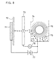
- FIG. 8 is a schematic sectional view showing an electric signal recording apparatus disclosed in the Japanese published examined patent application, Publication No. Sho 44-26333.
- toner 75 is negatively charged for example by friction with fur at the rotation of a brush 76.
- a power source 77 is connected across a mesh electrode 74 and a back electrode 71 to generate an electric field for accelerating the charged toner 75 toward a recording member 72.
- the amount of the toner 75 passing through the mesh electrode 74 and the adhesion position of the toner 75 to the recording member 72 can be controlled responding to the polarity and intensity of the applied electric signal 78.
- a parallel electric field for accelerating the toner 75 toward the recording member 72 is generated between the mesh electrode 74 and the back electrode 71 by the power source 77.
- FIG. 9 is a sectional view showing a schematic configuration of another image recording apparatus disclosed in the Japanese published examined patent application, Publication No. Hei 2-52260.
- a signal electrode 101 and a base electrode 103 are formed around a hole 104 with an insulator 102 disposed therebetween.
- a recording member 105 e.g. a paper, moves on the surface of a back electrode 106 disposed opposite to the signal electrode 101.
- the back electrode 106 is connected to a DC power source 109, and a voltage of about 300 V is applied to the back electrode 106.
- One-component insulating magnetic toner 111 is transferred from a toner transfer member 107 to an image forming position.
- An AC power source 108 is connected across the toner transfer member 107 and the base electrode 103.
- a signal source 110 is connected to the signal electrode 101 and the base electrode 103, and a recording voltage of 50 V is applied to the electrodes 101 and 103.
- the toner transfer member 107 is provided with a stationary magnet 112, and a magnetic blade 114 is provided in the vicinity of the toner transfer member 107.
- Thin layers of the one-component insulating magnetic toner 111 are formed on the toner transfer member 107 by the magnetic blade 114.
- an AC signal on which an AC or DC signal is superimposed is applied across the base electrode 103 and the toner transfer member 107, the one-component insulating magnetic toner 111 begins reciprocating or vibrating motion.
- the one-component insulating magnetic toner 111 passes through the hole 104, and adheres to the recording member 105 in accordance with an electric field applied to the back electrode 106.
- an image forming apparatus in accordance with the present invention comprises at least:
- charged particle jumping can be controlled by applying the voltage under the jumping start voltage lower than the charged particle jumping start voltage to the control electrodes, that is, by using signals having a small potential difference.
- low-voltage type switching devices can be used as switching devices for the power source, and the cost of the apparatus can be reduced.
- the image forming apparatus of the present invention may further comprise deflection electrodes each formed at least at a part of the fringe portion of the opening of the aperture electrode on the side of the back electrode and used to deflect the charged particles in the jumping direction in accordance with image information.
- the number of switching devices can be reduced significantly by controlling the movement direction of the charged particles by using the deflection electrodes.
- the image forming apparatus of the present invention may further comprise a control power source for outputting a control signal to the bias power source to control the charged particles passing through the openings in accordance with image information, whereby the bias power source superimposes a bias voltage on the control signal having been input and applies the jumping start voltage or the voltage under the jumping start voltage to the control electrodes.
- the image forming apparatus of the present invention may further comprise a stopping power source for applying a voltage having the same polarity as that of the charged particles to the control electrodes at the time when the charged particles are not sprinkled from the charged particle transfer means in accordance with image information.
- a stopping electrostatic field is generated after a printing electric field is generated, whereby the charged particles can be prevented from passing through the opening.
- An image forming method in accordance with the present invention comprises:
- the voltage under the jumping start voltage lower than the jumping start voltage for detaching the charged particles from the charged particle electrode is applied beforehand between the charged particle electrode and the control electrode. Therefore, the jumping of the charged particles can be controlled by using the signals having a small potential difference, and low-voltage type switching devices can be used as the switching devices for the power source.
- the image forming method of the present invention further comprises a step of deflecting the jumping direction of the charged particles in accordance with image information by using the deflection electrodes each formed at least at a part of the fringe portion of the opening of the aperture electrode on the side of the back electrode.
- the number of switching devices can be reduced significantly by controlling the movement direction of the charged particles by using the deflection electrodes.
- the image forming method of the present invention further comprises a step of outputting a control signal from the control power source to the bias power source to control the charged particles passing through the openings in accordance with image information, and a step of applying the jumping start voltage on which the bias voltage is superimposed and the voltage under the jumping start voltage to the control electrodes from the bias power source.
- the image forming method of the present invention further comprises a step of applying a voltage having the same polarity as that of the charged particles to the control electrodes at the time when the charged particles are not sprinkled from the charged particle transfer means in accordance with image information.
- a stopping electrostatic field is generated after a printing electric field is generated, whereby the charged particles can be prevented from passing through the opening.
- FIG. 1 is a schematic sectional view showing an image forming apparatus of embodiment 1 in accordance with the present invention.
- a development roller 2 used as a charged particle transfer means transfers toner used as charged particles.
- the development roller 2 in accordance with the embodiment 1 is formed of an aluminum cylinder having an outer diameter of 20 mm and a thickness of 1 mm, and the development roller 2 is grounded.
- the development roller 2 of the embodiment 1 is made of aluminum, it may be made of a metal, such as steel, or an alloy.
- the development roller 2 may be configured so that a DC or AC voltage is applied thereto.
- a control blade 4 is formed of an elastic material, such as urethane, having a hardness of 40 to 80 degrees (JIS K6301 A Scale).
- the length of the free end of the control blade 4 for controlling toner layers on the development roller 2 (the length of a portion extending from the installation member thereof) is in the range of 5 to 15 mm.
- the proper line pressure of the control blade 4 to the development roller 2 is in the range of 5 to 40 g/cm.
- One to three toner layers are formed on the development roller 2 by the pressure of the control blade 4.
- the control blade 4 is used in an electrically floating or grounded condition, or used with a DC or AC voltage applied thereto. In the case of the embodiment 1, the control blade 4 is used in the floating condition. Toner is held between the development roller 2 and the control blade 4, and is subjected to slight agitation therebetween, whereby the toner receives charges from the development roller 2 and is thus charged.
- a supply roller 2 making contact with the development roller 2 is formed of a shaft (8 mm in diameter in the embodiment 1) made of a metal, such as steel, which is coated with a layer of synthetic rubber, such as foamed urethane, having a thickness of about 2 to 6 mm.
- the hardness of the surface of the supply roller 6 is 30 degrees (when the material formed in the shape of a roller is measured in accordance with the method conforming to JIS K6301 A Scale).
- the biting amount of the supply roller 6 into the development roller 2 should preferably be in the range of 0.1 to 2 mm.
- the supply roller 6 is used in a grounded condition, or used with a DC or AC voltage applied thereto.
- the supply roller 6 assists in charging the toner and controls the supply of the toner.
- the embodiment 1 uses negatively charged toner.
- a back electrode 8 in the embodiment 1 is formed of a metal plate, it may be formed of a film formed of a conductive filler distributed in a resin. In this case, the resistance of the film should preferably in the range of about 10 2 to 10 10 ⁇ •cm.
- the toner is directly adhered onto the back electrode 8 to form the toner image, or a recording sheet 20 is placed on the back electrode 8, and the toner is adhered onto the recording sheet 20 to form the toner image.
- the back electrode 8 is formed in the shape of an endless film as described above, the toner is directly adhered onto the film, and the toner is transferred onto the recording sheet 20.
- the distance between the back electrode 8 and an aperture electrode described later should preferably be in the range of 50 to 1000 pm.
- An aperture electrode 12 is provided with a plurality of openings 14 formed in an insulating film and a plurality of control electrodes 16 correspond to the openings 14, respectively.
- the plural openings 14 and the plural control electrodes 16 of the aperture electrode 12 are arranged in a line from top to bottom of the sheet as seen in FIG. 1.
- the proper thickness of the insulating film of the aperture electrode 12 is in the range of 10 to 100 ⁇ m, and the film should preferably be made of polyimide, polyethylene terephthalate or the like.
- the numeral 22 represents a control power source
- the numeral 23 represents a bias power source
- the numeral 24 represents a stopping power source.
- FIG. 2 is a sectional view showing the structure of the aperture electrode 12 of the embodiment 1, and (b) of FIG. 2 is a plan view showing the aperture electrode 12.
- the control electrode 16 is formed in the shape of a ring so as to surround the fringe portion of the opening 14 as shown in (a) of FIG. 2.
- the control electrode 16 of the image forming apparatus of the present invention is not limited to the above-mentioned structure, but may be provided on the inner wall surface of the opening 14.
- a lead wire 18 extending from the control electrode 16 is connected to the control power source 22 and formed as a pattern trace on the insulating film.
- a thin resin layer (not shown) having a thickness of 1 to 10pm is formed on the surface of each control electrode 16.
- Two openings 14 being separate from each other are shown in (b) of FIG. 2. In actual practice, however, the plural openings 14 are disposed in a staggered arrangement.
- the openings 14 are disposed in the staggered arrangement so as to be supplementary to one another so that, when toner is sprayed from all the openings 14 to carry out recording, a completely black image can be formed.
- the diameter of the opening 14 should preferably be in the range of 50 to 200 ⁇ m. In the case of the embodiment 1, the diameter of the opening 14 is 150 ⁇ m, and the inner diameter of the opening 14 is 120 ⁇ m.
- the electrode portion of the control electrode 16 is made of a metal, such as copper, and its thickness should preferably be in the range of 5 to 30 ⁇ m.
- the control electrodes 16 are independently connected to the control power source 22 via the lead wires 18.
- the control power source 22 comprises a voltage generation portion (not shown) for generating voltages and switching devices for selecting the voltages by switching.
- a single switching device has about 32, 64 or 128 channels so that the voltages to be supplied to the control electrodes 16 via the lead wires 18 can be controlled individually.
- the voltages to be supplied to the control electrodes 16 via the lead wires 18 can be controlled individually.
- the control power source 22 comprises a voltage generation portion (not shown) for generating voltages and switching devices for selecting the voltages by switching.
- a single switching device has about 32, 64 or 128 channels so that the voltages to be supplied to the control electrodes 16 via the lead wires 18 can be controlled individually.
- 300 dpi dots per inch
- FIG. 3 shows the waveforms of voltages to be applied to the control electrode 16.
- the ordinate represents voltage
- the abscissa represents time.
- a period Tt represents the time required to form one dot and depends on resolution.
- the diameter of one dot is about 83 ⁇ m, which is obtained by dividing 1 inch, i.e. 25.4 mm, by 300 dots. While this one dot is formed, the recording sheet 20 should move by the length amounting to one dot. Accordingly, when the speed of the recording sheet 20 is 60 mm/s, for example, the period Tt is about 1390 ⁇ s.
- FIG. 3 shows a voltage waveform at the time when a voltage lower than a jumping start voltage is applied to the control electrode 16 in a period Ti.
- a constant distance condition for example, in a condition with respect to the distance between the aperture electrode 12 and the development roller 2
- dot formation starts at a constant applied voltage or more.
- This applied voltage is defined as the jumping start voltage
- a voltage lower than the jumping start voltage is defined as the voltage under the jumping start voltage. For this reason, while the voltage under the jumping start voltage is applied to the control electrode 16, toner is not sprinkled toward the back electrode 8, and nothing is printed.
- FIG. 4 shows the jumping start voltage to be applied to the control electrode 16.
- the abscissa represents voltage to be applied to the control electrode 16 and the ordinate represents dot image density.
- the period Ti shown in (a) of FIG. 3 can be a period arbitrarily determined within the period Tt, i.e., the time required to form one dot. This period Ti should preferably be shorter than a period Tb described later.
- the voltage under the jumping start voltage is applied from the bias power source 23 to the control electrode 16. This voltage under the jumping start voltage may be applied to all the control electrodes 16 regardless of the presence or absence of signals.
- a negative voltage is applied to the control electrode 16 after a lapse of the period Ti, and a stopping electrostatic field is generated to prevent toner from passing through the opening 14.
- (b) of FIG. 3 shows the waveform of a voltage applied to the control electrode 16 at the time of recording (at the time of toner jumping).
- a signal voltage (an image recording signal) exceeding the jumping start voltage is applied in a period Tb.
- This period Tb is required to be more than the time elapsed while toner is detached from the development roller 2 and reaches the back electrode 8.
- the period Tb is adjusted to the time during which the dot density is saturated, that is, 200 ⁇ s in the case of the embodiment 1. At this time, a bias electric field should be made synchronous with the alternating electric field generated by the signal voltage in view of reducing power consumption.
- a period Tw following the period Tb represents the time during which an electric field for preventing toner from being detached from the development roller 2 is generated.
- FIG. 5 is a schematic view showing the image forming apparatus of the embodiment 1.
- an intermediate transfer belt 30 used as an intermediate image holder is formed of a film in which a conductive filler is distributed in a resin, and the resistance of the intermediate transfer belt 30 is 10 10 ⁇ •cm.
- the back electrode 8 is disposed so as to make contact with the back side of the intermediate transfer belt 30 at the position opposite to the opening 14.
- a pickup roller 32 is provided to feed the recording sheets 20 one by one from a paper feed tray.
- a timing roller 34 is used to adjust the positional relationship between the recording sheet 20 being fed and the position of an image.
- a toner image formed on the intermediate transfer belt 30 is transferred from the transfer roller 36 to the recording sheet 20.
- the transfer roller 36 is formed of a metal roller coated with foamed sponge, such as urethane, and subjected to conductive treatment.
- the outer diameter of the transfer roller 36 is 20 mm, and the hardness of the roller is about 30 degrees in JIS K6301 A Scale. Both ends of the metal shaft of the transfer roller 36 are pressed against the intermediate transfer belt 30 at a pressure of about 500 to 1000 g. The electric resistance of the transfer roller 36 was measured when the roller was pressed at the above-mentioned pressure against a grounded metal plate, and 500 V was applied to the metal shaft. The resistance was in the range of about 10 6 to 10 7 ⁇ .
- a fixing device 38 fixes toner transferred to the recording sheet 20 by applying pressure and heat.
- the adhesion of the toner used for the embodiment 1 to the recording sheet 20 is carried out by heating and melting a resin.
- a styrene-acrylic-based copolymer is used as a resin.
- a styrene-butadiene-based copolymer, a polyester resin, an epoxy resin and resins made by mixing these can be used as toner.
- Magnetic toner including magnetic powder may be used as a matter of course. In this case, alloys and compounds, such as ferrite and magnetite, including elements displaying ferromagnetism, such as iron, cobalt and nickel, are effectively used as magnetic powder.
- the proper coercivity of the magnetic powder is in the range of 100 to 500 Oe. Furthermore, the proper amount of the magnetic powder to the resin is in the range of 20 to 40 weight % with respect to 100 weight % of toner particles.
- silica (SiO 2 ), titanium oxide (TiO 2 ), metal salt of stearic acid or the like in the range of 0.1 to 5 weight % should preferably be added to control the fluidity of a charge control agent and toner. In particular, silica greatly affects the fluidity, and can prevent the opening 14 from being clogged with toner.
- silica is small in diameter and highly chargeable, it is intensely attracted by electric forces and is liable to adhere to the inner wall surface of the opening 14. However, since the toner adhering to the inner wall surface of the opening 14 plays a role of rollers to accelerate the motion of toner passing through the opening 14, whereby hole clogging can be prevented.
- the BET specific surface area of silica due to nitrogen adsorption should be in the range of 100 to 300 m 2 /g. If silica having a smaller diameter of less than 100 m 2 /g, for example, is used, silica is mixed as if it cuts the resin to pieces, whereby toner cannot have sufficient fixing characteristics.
- the aperture 12 is provided with 300 openings 14 per inch. These openings 14 are arranged in lines from top to bottom of the sheet as seen in FIG. 5. The plural openings 14 are arranged at positions nearly opposite to the back electrode 8.
- the control electrodes 16 are formed at the fringe portions of the openings 14 corresponding thereto, and connected to the switching devices via the lead wires 18 (see (b) of FIG. 2).
- Each of the control electrodes 16 carries out image formation by combining the applied voltage waveforms shown in (a) and (b) of FIG. 3 and by transferring toner to the intermediate transfer belt 30.
- the distance between the development roller 2 and the aperture electrode 12 is about 50 ⁇ m
- the distance between the aperture electrode 12 and the back electrode 8 is about 150 ⁇ m.
- a voltage of about 1000 V is applied beforehand to the back electrode 8.
- a toner image formed on the intermediate transfer belt 30 is transferred to the recording sheet 20 being fed in synchronization with the toner image by applying about 500 V from behind the sheet.
- the toner image transferred onto the recording sheet 20 is fixed by the fixing device 38 and discharged outside the apparatus.
- a bias voltage lower than the voltage applied for detaching toner from the development roller 2 is applied beforehand between the development roller 2 and the control electrodes 16.
- toner jumping can be controlled by using signals having a small potential difference.
- low-voltage type switching devices can be used as the switching devices for the image forming apparatus of the embodiment 1.
- a large jumping electric field is generated in the openings 14 by the superimposing of the bias voltage and the signal voltage to prevent the openings 14 from being clogged with toner, thereby making it possible to attain proper image formation.
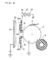
- FIG. 6 is a schematic sectional view showing the image forming apparatus of the embodiment 2.
- the components of the embodiment 2 having the same functions and configurations as those of the embodiment 1 are represented by the same reference codes and their explanations are omitted.
- the image forming apparatus of the embodiment 2 differs from the image forming apparatus of the embodiment 1 in that deflection electrodes 48 different from the control electrodes 16 is provided on the aperture electrode 12 on the side of the back electrode 8. Electrodes provided at such positions are disclosed in the Japanese published unexamined patent application, Publication No. Hei 4-189554, for example.
- the electrodes disclosed in the Japanese Publication No. Hei 4-189554 are control electrodes used to take out toner from the development roller.
- Each of the deflection electrodes 48 in the image forming apparatus of the embodiment 2 is used to change the transfer direction of toner sprinkled from the development roller 2. This change in direction is adjusted by a voltage applied to the deflection electrode 48.
- the voltage under the jumping start voltage, shown in (a) of FIG. 3, is applied to all the control electrodes 16 on the aperture electrode 12 at all times. Furthermore, the voltage shown in (b) of FIG. 3 is applied to the control electrode 16 disposed at positions corresponding to the image portions of image information. In the condition wherein the voltage shown in (b) of FIG. 3 is applied to the control electrode 16, an electric field for carrying out deflection by using the deflection electrode 48 is generated for the toner passed through the opening 14.
- the deflection electrode 48 is separated into an upper electrode 48a disposed at an upper position and a lower electrode 48b disposed at an lower position.
- the upper electrode 48a and the lower electrode 48b are independently connected to different power sources (not shown) and controlled. For example, when a voltage having an intensively negative polarity is applied to the upper electrode 48a of the deflection electrode 48 shown in FIG. 6, and a voltage having a weakly negative polarity is applied to the lower electrode 48b of the deflection electrode 48, negatively charged toner electrostatically repels the upper electrode 48a, and turns toward the lower electrode 48b.
- toner turns toward the upper electrode 48a.
- the transfer direction of the toner can be controlled in three directions, that is, in the upper, lower and straight directions from one opening 14.
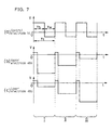
- FIG. 7 shows examples of the waveforms of voltages applied to the control electrode 16, and the upper electrode 48a and the lower electrode 48b of the deflection electrode 48, respectively.
- the voltage waveform shown in (a) of FIG. 7 is the waveform of the voltage applied to the control electrode 16, and is the same as the voltage waveform shown in (b) of FIG. 3.
- the voltage waveform shown in (b) of FIG. 7 is the waveform of the voltage applied to the upper electrode 48a of the deflection electrode 48.
- the voltage waveform shown in (c) of FIG. 7 is the waveform of the voltage applied to the lower electrode 48b of the deflection electrode 48.
- the abscissa represents time, and the ordinate represents voltage.
- the voltages applied to the upper electrode 48a and the lower electrode 48b of the deflection electrode 48 are described below in detail referring to FIG. 7.
- An intensively negative voltage (about -150 V in the embodiment 2) is applied to the upper electrode 48a of the deflection electrode 48 in a first dot forming period (a period represented by (I) in FIG. 7).
- a weakly negative voltage about -50 V in the embodiment 2 is applied to the lower electrode 48b of the deflection electrode 48.
- the same voltage (about -100 V in the embodiment 2) is applied to the upper electrode 48a and the lower electrode 48b.
- toner sprayed from the opening 14 moves straight without being bent by the deflection electrode 48.
- a weakly negative voltage (about -50 V) is applied to the upper electrode 48a, and an intensively negative voltage (about -150 V) is applied to the lower electrode 48b so that toner turns in the direction opposite to the deflection direction in the first dot forming period (the period represented by (I) in FIG. 7).
- an image forming control signal is not input to the control electrode 16, toner is not transferred toward the back electrode.
- the voltages having the waveforms shown in FIG. 7 should always be applied repeatedly to the deflection electrode 48 in such a manner as described above.
- the voltage waveforms in the present invention are not limited to those shown in FIG. 7, but the levels and timing of the voltages applied to the upper electrode 48a and the lower electrode 48b can be selectively determined depend on the distance and direction of deflection. Since the distance between the development roller 2 and the aperture electrode 12 is in the range of about 30 to 50 ⁇ m, for example, it takes about 20 to 40 ⁇ s until the time elapsed while toner is detached from the development roller 2 and reaches the opening 14. Therefore, the timing of applying voltages to the deflection electrode 48 may be delayed by 30 to 50 ⁇ s from the start of the dot forming period (the period Tt in (b) of FIG. 3).
- the image forming apparatus of the embodiment 2 is provided with the deflection electrode 48 on the aperture electrode 12 in the vicinity of the opening 14 and on the side of the back electrode as described above.
- dot forming and deflection can be controlled as desired, and plural dots can be formed from one opening 14.
- a significant cost reduction can be attained, for example, the number of switching devices can be reduced in the image forming apparatus of the embodiment 2.
- the image forming apparatus of the present invention configured as described above have the following effects.
- the image forming apparatus has a configuration capable of controlling toner jumping by using the signals having a small potential difference.
- low-voltage type switching devices can be used as the switching devices for the image forming apparatus of the present invention.
- the large jumping electric field is generated inside the opening by the superimposing of the bias voltage and the signal voltage, thereby preventing the opening from being clogged with charged particles.
- the present invention can provide an image forming apparatus and an image forming method capable of forming proper images.
- the image forming apparatus of the present invention is provided with the deflection electrode 48 formed at least at a part of the fringe portion of the opening 14 on the side of the back electrode and the deflection power sources for applying voltages to the deflection electrode 48. Therefore, the deflection electrode 48 generates a deflection electric field and controls the positions of charged particles to be received by the back electrode 8, whereby it is possible to form high-precision images.
Landscapes
- Printers Or Recording Devices Using Electromagnetic And Radiation Means (AREA)
- Developing For Electrophotography (AREA)
Applications Claiming Priority (2)
| Application Number | Priority Date | Filing Date | Title |
|---|---|---|---|
| JP7524898 | 1998-03-24 | ||
| JP7524898 | 1998-03-24 |
Publications (2)
| Publication Number | Publication Date |
|---|---|
| EP0945275A2 true EP0945275A2 (de) | 1999-09-29 |
| EP0945275A3 EP0945275A3 (de) | 1999-10-13 |
Family
ID=13570743
Family Applications (1)
| Application Number | Title | Priority Date | Filing Date |
|---|---|---|---|
| EP99302233A Withdrawn EP0945275A3 (de) | 1998-03-24 | 1999-03-23 | Gerät und Verfahren zur Erzeugung von Bildern |
Country Status (2)
| Country | Link |
|---|---|
| US (1) | US6286936B1 (de) |
| EP (1) | EP0945275A3 (de) |
Cited By (2)
| Publication number | Priority date | Publication date | Assignee | Title |
|---|---|---|---|---|
| EP1091264A1 (de) * | 1999-10-04 | 2001-04-11 | Agfa-Gevaert N.V. | Direkte elektrostatische Druckvorrichtung, wo geladene Tonerteilchen auf einem in Kontakt mit dem Tonerabgabeteil eines nichtmagnetisches Einkomponenten Entwicklungssystems Tonertransportgerät aufgetragen werden |
| EP0963852B1 (de) * | 1998-06-09 | 2001-05-16 | Agfa-Gevaert N.V. | Druckverfahren und Steuerung für Druckkopf mit Ablenkelektroden zum direkten elektrostatischen Drucken |
Families Citing this family (3)
| Publication number | Priority date | Publication date | Assignee | Title |
|---|---|---|---|---|
| US7292261B1 (en) * | 1999-08-20 | 2007-11-06 | Patrick Teo | Virtual reality camera |
| US8715029B2 (en) * | 2007-05-11 | 2014-05-06 | Forrest Frederick Bishop | Robotic construction cubes |
| KR101692585B1 (ko) * | 2013-10-18 | 2017-01-03 | 파나소닉 아이피 매니지먼트 가부시키가이샤 | 정전 도포 방법 및 정전 도포 장치 |
Citations (2)
| Publication number | Priority date | Publication date | Assignee | Title |
|---|---|---|---|---|
| JPS4426333B1 (de) | 1966-09-27 | 1969-11-05 | ||
| JPH0252260A (ja) | 1988-08-16 | 1990-02-21 | Fuji Electric Co Ltd | ディジタル電力量積算器 |
Family Cites Families (5)
| Publication number | Priority date | Publication date | Assignee | Title |
|---|---|---|---|---|
| US4491855A (en) | 1981-09-11 | 1985-01-01 | Canon Kabushiki Kaisha | Image recording method and apparatus |
| US5552814A (en) * | 1992-09-01 | 1996-09-03 | Brother Kogyo Kabushiki Kaisha | Image recording apparatus wherein toner carrier member and particle-flow modulating electrode member are held in contact with each other |
| US5781218A (en) | 1996-02-06 | 1998-07-14 | Sharp Kabushiki Kaisha | Image forming apparatus |
| US5847733A (en) | 1996-03-22 | 1998-12-08 | Array Printers Ab Publ. | Apparatus and method for increasing the coverage area of a control electrode during direct electrostatic printing |
| US5984456A (en) * | 1996-12-05 | 1999-11-16 | Array Printers Ab | Direct printing method utilizing dot deflection and a printhead structure for accomplishing the method |
-
1999
- 1999-03-23 US US09/274,794 patent/US6286936B1/en not_active Expired - Fee Related
- 1999-03-23 EP EP99302233A patent/EP0945275A3/de not_active Withdrawn
Patent Citations (2)
| Publication number | Priority date | Publication date | Assignee | Title |
|---|---|---|---|---|
| JPS4426333B1 (de) | 1966-09-27 | 1969-11-05 | ||
| JPH0252260A (ja) | 1988-08-16 | 1990-02-21 | Fuji Electric Co Ltd | ディジタル電力量積算器 |
Cited By (2)
| Publication number | Priority date | Publication date | Assignee | Title |
|---|---|---|---|---|
| EP0963852B1 (de) * | 1998-06-09 | 2001-05-16 | Agfa-Gevaert N.V. | Druckverfahren und Steuerung für Druckkopf mit Ablenkelektroden zum direkten elektrostatischen Drucken |
| EP1091264A1 (de) * | 1999-10-04 | 2001-04-11 | Agfa-Gevaert N.V. | Direkte elektrostatische Druckvorrichtung, wo geladene Tonerteilchen auf einem in Kontakt mit dem Tonerabgabeteil eines nichtmagnetisches Einkomponenten Entwicklungssystems Tonertransportgerät aufgetragen werden |
Also Published As
| Publication number | Publication date |
|---|---|
| EP0945275A3 (de) | 1999-10-13 |
| US6286936B1 (en) | 2001-09-11 |
Similar Documents
| Publication | Publication Date | Title |
|---|---|---|
| US5038159A (en) | Apertured printhead for direct electrostatic printing | |
| US5214451A (en) | Toner supply leveling in multiplexed DEP | |
| CA1326055C (en) | Printing apparatus and toner/developer delivery system therefor | |
| US4912489A (en) | Direct electrostatic printing apparatus with toner supply-side control electrodes | |
| US5095322A (en) | Avoidance of DEP wrong sign toner hole clogging by out of phase shield bias | |
| US5966151A (en) | Image forming apparatus | |
| US5040004A (en) | Belt donor for direct electrostatic printing | |
| US5327169A (en) | Masked magnetic brush direct writing for high speed and color printing | |
| US6286936B1 (en) | Image forming apparatus and image forming method | |
| EP0501739B1 (de) | Elektrostatisches Druckgerät und Verfahren | |
| GB1586277A (en) | Nonimpact printer with magnetic ink reorientation | |
| US6011944A (en) | Printhead structure for improved dot size control in direct electrostatic image recording devices | |
| EP0415701B1 (de) | Druckgerät und Verfahren zur Bilderzeugung auf einem Substrat | |
| JPH11334137A (ja) | 画像形成装置及び画像形成方法 | |
| US6296348B1 (en) | Direct recording apparatus with controlling section to adjust voltage among discharge electrodes | |
| US6601946B1 (en) | Image forming apparatus in which toner is removed by changing electric field between opposing electrode and control electrode | |
| US6144394A (en) | Image forming method and device | |
| US6817701B2 (en) | Image forming apparatus | |
| WO2001026906A1 (en) | Image forming method and image forming apparatus | |
| WO2001064446A1 (en) | Print head, and image forming device using the same | |
| JPH11277790A (ja) | 画像形成方法及び画像形成装置 | |
| JP2003034048A (ja) | 画像形成装置 | |
| JP2001287392A (ja) | プリントヘッド及び該プリントヘッドを用いた画像形成装置 | |
| JPWO2001026906A1 (ja) | 画像形成方法及び画像形成装置 | |
| JP2001277578A (ja) | プリントヘッド、プリントヘッドの製造方法及び画像形成装置 |
Legal Events
| Date | Code | Title | Description |
|---|---|---|---|
| PUAI | Public reference made under article 153(3) epc to a published international application that has entered the european phase |
Free format text: ORIGINAL CODE: 0009012 |
|
| PUAL | Search report despatched |
Free format text: ORIGINAL CODE: 0009013 |
|
| 17P | Request for examination filed |
Effective date: 19990409 |
|
| AK | Designated contracting states |
Kind code of ref document: A2 Designated state(s): DE FR GB |
|
| AX | Request for extension of the european patent |
Free format text: AL;LT;LV;MK;RO;SI |
|
| AK | Designated contracting states |
Kind code of ref document: A3 Designated state(s): AT BE CH CY DE DK ES FI FR GB GR IE IT LI LU MC NL PT SE |
|
| AX | Request for extension of the european patent |
Free format text: AL;LT;LV;MK;RO;SI |
|
| RAP1 | Party data changed (applicant data changed or rights of an application transferred) |
Owner name: ARRAY PRINTERS AB Owner name: MATSUSHITA ELECTRIC INDUSTRIAL CO., LTD. |
|
| AKX | Designation fees paid |
Free format text: DE FR GB |
|
| RAP1 | Party data changed (applicant data changed or rights of an application transferred) |
Owner name: ARRAY AB Owner name: MATSUSHITA ELECTRIC INDUSTRIAL CO., LTD. |
|
| GRAH | Despatch of communication of intention to grant a patent |
Free format text: ORIGINAL CODE: EPIDOS IGRA |
|
| STAA | Information on the status of an ep patent application or granted ep patent |
Free format text: STATUS: THE APPLICATION IS DEEMED TO BE WITHDRAWN |
|
| 18D | Application deemed to be withdrawn |
Effective date: 20021224 |