EP0945525A1 - Beschichtungs-Verfahren und -Vorrichtung - Google Patents
Beschichtungs-Verfahren und -Vorrichtung Download PDFInfo
- Publication number
- EP0945525A1 EP0945525A1 EP99102284A EP99102284A EP0945525A1 EP 0945525 A1 EP0945525 A1 EP 0945525A1 EP 99102284 A EP99102284 A EP 99102284A EP 99102284 A EP99102284 A EP 99102284A EP 0945525 A1 EP0945525 A1 EP 0945525A1
- Authority
- EP
- European Patent Office
- Prior art keywords
- laser
- lasers
- coating
- light emitted
- parameter
- Prior art date
- Legal status (The legal status is an assumption and is not a legal conclusion. Google has not performed a legal analysis and makes no representation as to the accuracy of the status listed.)
- Granted
Links
- 238000000576 coating method Methods 0.000 title claims abstract description 89
- 239000011248 coating agent Substances 0.000 claims abstract description 78
- 238000000034 method Methods 0.000 claims abstract description 52
- 238000011065 in-situ storage Methods 0.000 claims abstract description 20
- 238000002310 reflectometry Methods 0.000 claims abstract description 11
- 239000004065 semiconductor Substances 0.000 claims description 32
- 230000008569 process Effects 0.000 claims description 20
- 230000003667 anti-reflective effect Effects 0.000 claims description 10
- 238000004519 manufacturing process Methods 0.000 claims description 8
- 230000003287 optical effect Effects 0.000 claims description 8
- 230000015572 biosynthetic process Effects 0.000 claims 1
- 239000010410 layer Substances 0.000 description 35
- 239000006117 anti-reflective coating Substances 0.000 description 10
- 238000013461 design Methods 0.000 description 9
- 241000538562 Banjos Species 0.000 description 2
- 230000008901 benefit Effects 0.000 description 2
- 239000003365 glass fiber Substances 0.000 description 2
- 230000006872 improvement Effects 0.000 description 2
- 239000000463 material Substances 0.000 description 2
- 238000012986 modification Methods 0.000 description 2
- 230000004048 modification Effects 0.000 description 2
- 238000012544 monitoring process Methods 0.000 description 2
- 239000002356 single layer Substances 0.000 description 2
- 230000003321 amplification Effects 0.000 description 1
- 239000002800 charge carrier Substances 0.000 description 1
- 230000008021 deposition Effects 0.000 description 1
- 238000000572 ellipsometry Methods 0.000 description 1
- 238000005516 engineering process Methods 0.000 description 1
- 238000004868 gas analysis Methods 0.000 description 1
- 238000005305 interferometry Methods 0.000 description 1
- 230000007246 mechanism Effects 0.000 description 1
- 238000003199 nucleic acid amplification method Methods 0.000 description 1
- 238000005457 optimization Methods 0.000 description 1
- 238000002161 passivation Methods 0.000 description 1
- 238000004886 process control Methods 0.000 description 1
- 238000012549 training Methods 0.000 description 1
- 238000012546 transfer Methods 0.000 description 1
Images



Classifications
-
- C—CHEMISTRY; METALLURGY
- C23—COATING METALLIC MATERIAL; COATING MATERIAL WITH METALLIC MATERIAL; CHEMICAL SURFACE TREATMENT; DIFFUSION TREATMENT OF METALLIC MATERIAL; COATING BY VACUUM EVAPORATION, BY SPUTTERING, BY ION IMPLANTATION OR BY CHEMICAL VAPOUR DEPOSITION, IN GENERAL; INHIBITING CORROSION OF METALLIC MATERIAL OR INCRUSTATION IN GENERAL
- C23C—COATING METALLIC MATERIAL; COATING MATERIAL WITH METALLIC MATERIAL; SURFACE TREATMENT OF METALLIC MATERIAL BY DIFFUSION INTO THE SURFACE, BY CHEMICAL CONVERSION OR SUBSTITUTION; COATING BY VACUUM EVAPORATION, BY SPUTTERING, BY ION IMPLANTATION OR BY CHEMICAL VAPOUR DEPOSITION, IN GENERAL
- C23C14/00—Coating by vacuum evaporation, by sputtering or by ion implantation of the coating forming material
- C23C14/22—Coating by vacuum evaporation, by sputtering or by ion implantation of the coating forming material characterised by the process of coating
- C23C14/50—Substrate holders
-
- C—CHEMISTRY; METALLURGY
- C23—COATING METALLIC MATERIAL; COATING MATERIAL WITH METALLIC MATERIAL; CHEMICAL SURFACE TREATMENT; DIFFUSION TREATMENT OF METALLIC MATERIAL; COATING BY VACUUM EVAPORATION, BY SPUTTERING, BY ION IMPLANTATION OR BY CHEMICAL VAPOUR DEPOSITION, IN GENERAL; INHIBITING CORROSION OF METALLIC MATERIAL OR INCRUSTATION IN GENERAL
- C23C—COATING METALLIC MATERIAL; COATING MATERIAL WITH METALLIC MATERIAL; SURFACE TREATMENT OF METALLIC MATERIAL BY DIFFUSION INTO THE SURFACE, BY CHEMICAL CONVERSION OR SUBSTITUTION; COATING BY VACUUM EVAPORATION, BY SPUTTERING, BY ION IMPLANTATION OR BY CHEMICAL VAPOUR DEPOSITION, IN GENERAL
- C23C14/00—Coating by vacuum evaporation, by sputtering or by ion implantation of the coating forming material
- C23C14/22—Coating by vacuum evaporation, by sputtering or by ion implantation of the coating forming material characterised by the process of coating
- C23C14/54—Controlling or regulating the coating process
- C23C14/542—Controlling the film thickness or evaporation rate
- C23C14/545—Controlling the film thickness or evaporation rate using measurement on deposited material
- C23C14/547—Controlling the film thickness or evaporation rate using measurement on deposited material using optical methods
-
- H—ELECTRICITY
- H01—ELECTRIC ELEMENTS
- H01S—DEVICES USING THE PROCESS OF LIGHT AMPLIFICATION BY STIMULATED EMISSION OF RADIATION [LASER] TO AMPLIFY OR GENERATE LIGHT; DEVICES USING STIMULATED EMISSION OF ELECTROMAGNETIC RADIATION IN WAVE RANGES OTHER THAN OPTICAL
- H01S5/00—Semiconductor lasers
- H01S5/02—Structural details or components not essential to laser action
- H01S5/028—Coatings ; Treatment of the laser facets, e.g. etching, passivation layers or reflecting layers
-
- H—ELECTRICITY
- H01—ELECTRIC ELEMENTS
- H01S—DEVICES USING THE PROCESS OF LIGHT AMPLIFICATION BY STIMULATED EMISSION OF RADIATION [LASER] TO AMPLIFY OR GENERATE LIGHT; DEVICES USING STIMULATED EMISSION OF ELECTROMAGNETIC RADIATION IN WAVE RANGES OTHER THAN OPTICAL
- H01S5/00—Semiconductor lasers
- H01S5/0014—Measuring characteristics or properties thereof
Definitions
- the present invention relates to a method for producing Antireflection coatings (hereinafter also referred to as AR layers) for semiconductor lasers according to the preamble of claim 1.
- AR layers Antireflection coatings
- Anti-reflective semiconductor laser diodes are used in modern optical measuring instruments used for gas analysis and interferometry or as optical radar. Other applications are in the field of active light amplification.
- semiconductor lasers Due to the jump in refractive index between the laser material and the environment, semiconductor lasers have a reflectivity of the mirror facets of typically 32%.
- a common method for the anti-reflective treatment of one or both laser facets is to coat them with a dielectric layer with a thickness which corresponds to a quarter of the central wavelength of the laser.
- the value of the refractive index is chosen according to the harmonic mean of the refractive index of the laser material and the environment. With a suitable control of the thickness and value of the refractive index of the anti-reflective coating, values of the minimum residual reflectivity of less than 10 -5 can be achieved. Several methods for this are known in the literature.
- P the light power emitted by the rear laser facet
- J the standardized threshold current density
- ⁇ the electron decay rate
- N the transparency charge carrier density
- G N the differential gain
- I th the standardized threshold current density of the laser
- v g the group speed of the light
- L the length of the Lasers
- r 12 the reflectivity of the interface between the AR layer and the laser
- r 23 the reflectivity between the AR layer and the surroundings
- n 2 ⁇ h the optical layer thickness of the antireflection layer with the refractive index n 2 and the geometric thickness h and ⁇ the central wavelength of the laser.
- the other laser parameters can be determined using the same formalism.
- Modern high-performance laser diodes generally have an anti-reflective coating on a laser facet with a reflectivity of typically 5% to 10%.
- High-quality anti-reflective coating cannot therefore be achieved by growing a single anti-reflective coating.
- To produce high-quality anti-reflective coatings it is then necessary either to remove the precoating or to grow at least two layers of different thickness and different refractive index.
- M. Dagenais and I-Fan Wu proposed that an in-situ ellipsometer be used to control the removal process of the precoating or to control the layer thicknesses that had grown.
- the problem is what an economic use precludes the application of this method in addition to the high cost of the meter that this has to be adjusted on a measuring point of typically 10 ⁇ m x 10 ⁇ m.
- the invention is based on a method for producing AR layers with in-situ observation of the light emitted by the front facet and / or rear facet of the laser, the electrical voltage at the pn junction of the laser or the quantum efficiency of that of the front facet and / or the laser light emitted by the back facet of the laser or the threshold current of the laser and, according to the characterizing part of claim 1, provides that the thickness of the AR layers is determined by the course of a laser parameter observed in situ .
- the observed measured values are thus measured in situ, for example with the theoretical values according to Eq. (1) or Eq. (2) compared; the thickness of the respective sub-layer is determined directly from this.
- laser parameters are named for the method can be used.
- these are the services of the Front and / or the back facet of the laser emitted light, the quantum efficiency the one emitted by the front and / or back facet of the laser Light, the wavelength of the light emitted by the laser, the electrical Voltage at the p-n junction of the laser and the threshold current of the laser.
- the One or more of the laser parameters can be within the scope of the invention used to determine the layer thickness of one or more sub-layers become.
- Claims 15 to 18 define the designs in which the lasers in the Recipients are introduced.
- Claims 19 to 28 define important features of the device for Implementation of the process for the anti-reflection coating of semiconductor lasers.
- the device is in accordance with independent claim 19 from a recipient, the at least one coating source, one or several holders for semiconductor lasers, one or more diaphragms one Control and measuring device and connecting lines contains.
- each coating source at least assigned a movable laser holder for coating the laser diode is.
- At least one aperture is located in front of the laser holder the laser or lasers selectively releases what is individually or collectively can be effected.
- the recipient has a magazine part in which the Coating or coated lasers are included in the coating part of the recipient are transferable.
- This assembly - magazine part and coating part - can be structurally identical.
- Claim 21 describes a very elegant form for this transfer process, by a swiveling and / or slidable aperture holder is arranged. This turns the laser magazine practically part of the coating chamber; so you don't need any elaborate motor-driven sled or similar mechanisms.
- the lasers are arranged relative to the coating source.
- the order is appropriately adapted to the coating parameters, in particular Growth rate and refractive index. It is especially advantageous if all lasers on a line with an identical coating rate and an identical refractive index lie.
- the coating parameters are often related to the Coating source is rotationally symmetrical. Claim 22 provides that the lasers are arranged in a ring or a circle. This ensures that everyone Laser experiences the same coating rate and the applied layers get the same refractive index. Another common case is that the coating parameters are linear over a certain range Possess symmetry; then the lasers should be arranged linearly according to claim 23 be.
- Claim 24 provides that one or more screens during the anti-reflective process fully or partially movable in front of or each laser are. This enables an individual optimization of each laser by during coating individual lasers or all but one laser Covers are covered.
- more than one laser is electrical during the process operable, wherein according to claim 26 devices for measuring or observing the laser parameters can be present in such training that with at least one laser, preferably with several or all in the Lasers containing lasers contain at least one laser parameter continuously or is discreetly observable, creating a high level of efficiency and Process security is guaranteed.
- a control and measuring device is used for process control, which with a laser control, a regulation for the control of the Apertures in the recipient, a layer control and a vacuum control is provided. All electronics are preferably in one separate control cabinet and is according to claim 28 via electrical and / or optical lines with the coating source, the laser holder and / or of the aperture holder in the recipient.
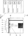
- a coating system for semiconductor lasers is shown schematically. It consists of a recipient 1 in which the coating process takes place, and a control and measuring device 9, all process-relevant Checked parameters.
- the recipient is 1 in an upper magazine part 11 and a coating part located underneath 14 divided.
- a coating source 2 on the Bottom of the recipient 1 arranged.
- Semiconductor lasers 3 are in a laser holder 4 mounted, which is located on a carrier plate 6.
- the semiconductor laser 3 are covered with at least one screen 5, which is attached to a bracket 15 is attached and is used for the individual release of the individual lasers.
- the entire laser unit 3, 4 can be covered by an aperture 5 become.
- Control unit 9 has a modular structure. It exists, as schematically on the right in FIG. 1 is indicated, from a laser control 901, from an aperture control 921, a shift control unit 941 and a vacuum control 961. These units are with coating source 2, the laser mount 4 and / or the panel holder 15, e.g. by electrical and / or optical lines 19.
- Drawing file 2A shows the time profile of the light power P for a single-layer anti-reflective coating. The best value of the anti-reflective coating is in the area of the minimum reached.
- Part 2B shows the course of the threshold current 1 for a one-layer anti-reflective coating. The best value is in the range of the maximum achieved.
- Part 2C shows the course of the voltage U at the p-n junction of the Lasers, also for a single-layer anti-reflective coating. Again, the best Value in the range of the maximum reached.
- Fig. 3 shows the course of the growth rate R as a function of the location, relative to Coating source.
- the coating rate can be seen from partial image 3A as Function of the radius of a rotationally symmetrical to the coating source arranged laser holder.
- the invention provides that Laser in this case on a circle or ring with the same growth rate to be arranged (see FIGS. 5 to 7).
- the course of the coating rate for a coating source over a The area having translation-invariant geometry is from the partial images 3B and 3C.
- Fig. 4 shows two schematic representations of the attachment.
- the semiconductor laser 3 are in the laser holder 4 e.g. screwed with a banjo bolt 321.
- the front facet 302 of a laser chip 301 is aligned such that the dielectric coating is reflected on it.
- the back one Facet 303 of laser chip 301 faces away from the coating.
- a photodiode 310 is mounted behind the laser, with which the laser light emitted from the rear laser facet 303 is observed.
- 4B instead of the photodiode 310, a glass fiber 311 is behind the Laser 3 attached, with which the emitted from the rear laser facet 303 Light led out of the recipient 1 for a more detailed observation becomes.
- FIG. 5 shows schematically a preferred design of the laser holder or Laser magazine 4 for rotationally symmetrical coating.
- Fig. 5A shows a plan view of the laser holder 4 together with the arrangement of the diaphragms 5; a cross section of the arrangement can be seen in FIG. 5B.
- the semiconductor laser 3 are on a line 410 with the same coating rate and the same Refractive index arranged.
- Each laser 3 can be individually from an aperture 5 covered or by translating the aperture 5 in the direction of arrow 51 to Coating are released. To the movement of the aperture 5 in the direction realizing the arrow, you can use the cover on a sliding carriage Place 52 or 53 driven by a stepper motor (not shown) becomes.
- Laser 35 is covered by aperture 55 and thus before coating protected.
- FIG. 6 schematically shows a further preferred design of the laser holder or laser magazine 4 for rotationally symmetrical coating.
- 6A shows a plan view of the laser holder 4 together with the arrangement of the aperture 5 .; a cross section of the arrangement is shown in Fig. 6B.
- the semiconductor laser 3 are here on a line 410 with the same coating rate and the same Refractive index arranged.
- Aperture 5 can fully according to arrow 59 Moved side to release all lasers 3 simultaneously for coating.
- aperture 5 is positioned in front of laser holder 4, there is an opening 57 exactly one laser 3 or 36 free.
- Arrow 58 each laser 3 can be released individually for coating.
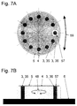
- FIG. 7 A modification can be seen from Fig. 7, wherein not the aperture, but the Laser holder 4 is rotatably arranged according to arrow 48.
- the coating process is otherwise equivalent to that described for FIG. 6.
- Fig. 8 shows a schematic representation of a preferred design of the Laser holder or laser magazine 4 for translational symmetrical coating.
- 8A shows a top view of the laser holder 4 together with the Arrangement of panels 5;
- 8B shows a longitudinal section of the arrangement.
- the Semiconductor lasers 3 are along two lines 411 with the same coating rate and the same refractive index.
- Each laser 3 can individually by an aperture 5 covered or by translating the aperture 5 in the direction of Arrow 51 are released for coating.
- laser is 35 covered by aperture 55 and thus protected from coating.
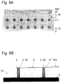
- FIG. 9 shows a modified design of the laser holder or laser magazine 4 schematically shown for translational symmetrical coating.
- Figure 9A shows a plan view of the laser holder 4 together with the aperture 5;
- Figure 9B shows the arrangement in longitudinal section.
- the semiconductor lasers 3 are along two Lines 411 with the same coating rate and the same refractive index arranged.
- Aperture 5 is movable to the side in the direction of arrow 585, so that all Laser 3 are released for coating at the same time.
- an opening 57 gives exactly one laser 3 or 36 free for coating.
- Aperture 5 can also according to arrow 585 be displaceable so that each laser 3 is released individually for coating becomes.
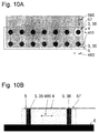
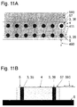
- the aperture 5 in the direction of an arrow 590 and the laser holder is displaceable in the direction of an arrow 490, as in FIG. 11 shown.
- the laser light emitted by the front facet and / or rear facet of a laser is observed in situ and the thickness of individual partial layers is determined on the basis of a laser parameter observed in situ , in particular by comparison with one theoretically calculated time course.
- the power or the quantum efficiency of the light emitted by the laser can be used as laser parameters, optionally also its wavelength, the electrical voltage at the pn junction of the laser or its threshold current.
- a particularly suitable device comprises at least one movable laser holder 4 and / or at least one aperture 5 located in front of it, which can optionally be moved in front of the or each laser 3 during the anti-reflective treatment.
- the lasers 3 can be arranged in a ring, circular or linear manner. At least one can be operated electrically in the recipient 1 and can be continuously or discretely observed for at least one laser parameter by means of a control and measuring device 9.
- a control cabinet can contain a laser control 901, an aperture control 921, a layer control 941 and / or a vacuum control 961.
- the control and measuring device 9, ie the control electronics, is actuation-connected to the coating source 2, the laser holder 4 and / or the aperture holder 5, for example by electrical and / or optical lines 19.
Landscapes
- Chemical & Material Sciences (AREA)
- Chemical Kinetics & Catalysis (AREA)
- Engineering & Computer Science (AREA)
- Materials Engineering (AREA)
- Mechanical Engineering (AREA)
- Metallurgy (AREA)
- Organic Chemistry (AREA)
- Physics & Mathematics (AREA)
- Condensed Matter Physics & Semiconductors (AREA)
- General Physics & Mathematics (AREA)
- Electromagnetism (AREA)
- Optics & Photonics (AREA)
- Semiconductor Lasers (AREA)
Abstract
Description
- Fig. 1
- eine schematische Darstellung einer Beschichtungsanlage für Halbleiterlaser,
- Fig. 2A
- ein typischer Verlauf der Lichtleistung eines Lasers während eines Entspiegelungsprozesses,
- Fig. 2B
- ein typischer Verlauf des Schwellstroms eines Lasers während eines Entspiegelungsprozesses,
- Fig. 2C
- ein typischer Verlauf der Spannung am p-n-Übergang eines Lasers während eines Entspiegelungsprozesses,
- Fig. 3A bis 3 C
- schematische Darstellungen der Wachstumsrate aufgebrachter Schichten bei rotationssymmetrischen bzw. linearen Beschichtungsparametern,
- Fig. 4A und 4B
- je eine schematische Darstellung bevorzugter Bauformen der Befestigung des Halbleiterlasers im Laserhalter,
- Fig. 5 bis 7
- schematische Darstellungen - jeweils mit Teilbildern - bevorzugter Bauformen eines Laserhalters für rotationssymmetrische Beschichtung und Blendenanordnung, und
- Fig. 8 bis 11
- schematische Darstellungen - jeweils mit Teilbildern - bevorzugter Bauformen eines Laserhalters für translationssymmetrische Beschichtung und Blendenanordnung.
- 1
- Rezipient
- 2
- Beschichtungsquelle
- 3
- (Halbleiter-)Laser
- 4
- Laserhalterung/-Magazin
- 5
- Blende
- 6
- Trägerplatte
- 9
- Steuerungs- und Meßeinrichtung
- 11
- Magazinteil
- 14
- Beschichtungsteil
- 15
- Blendenhalterung
- 19
- Leitungen
- 35, 36
- Laser
- 48, 51
- Pfeilrichtung
- 52, 53
- Blendenträger/Schlitten
- 55, 56
- Blenden
- 57
- Öffnung
- 58, 59
- Pfeilrichtung
- 301
- Laserchip
- 302
- Fronfacette
- 303
- Rückfacette
- 310
- Photodiode
- 311
- Glasfaser/Lichtleiter
- 321
- Hohlschraube
- 410, 411
- Linien
- 480, 490
- Pfeilrichtungen
- 580, 585, 590
- Pfeilrichtungen
- 901
- Laser-Ansteuerung
- 921
- Blendenregelung
- 941
- Schichtkontrolle(einheit)
- 961
- Vakuumkontrolle(einheit)
Claims (28)
- Verfahren zur Herstellung von Antireflexions-Schichten von minimaler Restreflektivität für Halbleiterlaserdioden mit in-situ-Beobachtung des von der Frontfacette und/oder Rückfacette eines Lasers emittierten Laserlichts, der elektrischen Spannung am p-n-Übergang des Lasers oder der Quanteneffizienz des von der Frontfacette und/oder des von der Rückfacette des Lasers emittierten Laserlichts oder des Schwellstroms des Lasers, dadurch gekennzeichnet, daß die Dicke der einzelnen Teilschichten, aus denen sich die Antireflexions-Beschichtung zusammensetzt, durch den in-situ-beobachteten Verlauf eines Laserparameters bestimmt wird.
- Verfahren nach Anspruch 1, gekennzeichnet durch den Vergleich des theoretisch berechneten Zeitverlaufs des Laserparameters mit dem in situ beobachteten Zeitverlauf.
- Verfahren nach Anspruch 1 oder 2, dadurch gekennzeichnet, daß der Laserparameter die Leistung des von der Frontfacette des Lasers emittierten Lichts ist.
- Verfahren nach Anspruch 1 oder 2, dadurch gekennzeichnet, daß der Laserparameter die Leistung des von der Rückfacette des Lasers emittierten Lichts ist.
- Verfahren nach Anspruch 1 oder 2, dadurch gekennzeichnet, daß der Laserparameter die Leistung des von der Front- und der Rückfacette des Lasers emittierten Lichts ist.
- Verfahren nach Anspruch 1 oder 2, dadurch gekennzeichnet, daß der Laserparameter die Quanteneffizienz des von der Frontfacette des Lasers emittierten Lichts ist.
- Verfahren nach Anspruch 1 oder 2, dadurch gekennzeichnet, daß der Laserparameter die Quanteneffizienz des von der Rückfacette des Lasers emittierten Lichts ist.
- Verfahren nach Anspruch 1 oder 2, dadurch gekennzeichnet, daß der Laserparameter die Quanteneffizienz des von der Front- und der Rückfacette des Lasers emittierten Lichts ist.
- Verfahren nach Anspruch 1 oder 2, dadurch gekennzeichnet, daß der Laserparameter die Wellenlänge des vom Laser emittierten Lichts ist.
- Verfahren nach Anspruch 1 oder 2, dadurch gekennzeichnet, daß der Laserparameter die elektrische Spannung am p-n-Übergang des Lasers ist.
- Verfahren nach Anspruch 1 oder 2, dadurch gekennzeichnet, daß der Laserparameter der Schwellstrom des Lasers ist.
- Verfahren nach einem der Ansprüche 1 bis 11, dadurch gekennzeichnet, daß man mehrere Halbleiterdiodenlaser gleichzeitig in einen Rezipienten einbringt.
- Verfahren nach einem der Ansprüche 1 bis 12, dadurch gekennzeichnet, daß ein Laser als Monitorlaser benutzt wird und weitere Laser simultan mitbeschichtet werden.
- Verfahren nach Anspruch 12 oder 13, dadurch gekennzeichnet, daß bei mindestens einer Teilschicht alle im Rezipienten eingebrachten Halbleiterlaser gemeinsam bis zu einem Referenzwert beschichtet werden, worauf man die Schichtdicke jedes Lasers einzeln mit in-situ-Beobachtung eines oder mehrerer Laserparameter optimiert.
- Verfahren nach einem der Ansprüche 12 bis 14, dadurch gekennzeichnet, daß man alle Laser fertig konfektioniert in den Rezipienten einbringt.
- Verfahren nach einem der Ansprüche 12 bis 14, dadurch gekennzeichnet, daß mindestens ein fertig konfektionierter Laser und im übrigen nicht fertig konfektionierte Laser in den Rezipienten eingebracht werden.
- Verfahren nach Anspruch 16, dadurch gekennzeichnet, daß die nicht fertig konfektionierten Laser in Chipform in den Rezipienten eingebracht werden.
- Verfahren nach Anspruch 16, dadurch gekennzeichnet, daß die nicht fertig konfektionierten Laser in Barrenform in den Rezipienten eingebracht werden.
- Vorrichtung zum Herstellen von Antireflexionsschichten von minimaler Restreflektivität für Halbleiterdiodenlaser mit in-situ-Beobachtung des von der Frontfacette und/oder Rückfacette eines Lasers (3) emittierten Laserlichts, der elektrischen Spannung am p-n-Übergang des Lasers oder der Quanteneffizienz des von der Frontfacette und/oder Rückfacette des Lasers emittierten Laserlichts oder des Schwellstroms des Lasers, mit einem Rezipienten (1), mit einer Beschichtungsquelle (2) und mit wenigstens einem zu beschichtenden, in einer Halterung (4) gefaßten Laser (3), insbesondere zur Durchführung des Verfahrens nach einem der Ansprüche 1 bis 18, dadurch gekennzeichnet, daß der Beschichtungsquelle (2) mindestens eine bewegliche Laser-Halterung (4) und/oder mindestens eine vor der bzw. jeder Laserhalterung (4) befindliche, wahlweise bewegbare Blende (5) zugeordnet ist.
- Vorrichtung nach Anspruch 19, dadurch gekennzeichnet, daß der bzw. jeder Laser (3) zusammen mit seiner als Magazin (11) ausgebildeten Halterung in eine Beschichtungskammer (14) überführbar ist.
- Vorrichtung nach Anspruch 19 oder 20, dadurch gekennzeichnet, daß der bzw. jeder Laser (3) sich in einer Beschichtungskammer (14) befindet, neben der eine schwenk- und/oder verschiebbare Blendenhalterung (17) angeordnet ist.
- Vorrichtung nach einem der Ansprüche 19 bis 21, dadurch gekennzeichnet, daß die Laser (3) ring- oder kreisförmig angeordnet sind.
- Vorrichtung gemäß einem der Ansprüche 19 bis 21, dadurch gekennzeichnet, daß die Laser (3) linear angeordnet sind.
- Vorrichtung gemäß einem der Ansprüche 19 bis 23, dadurch gekennzeichnet, daß eine oder mehrere Blenden (5) während des Entspiegelungsprozesses ganz oder teilweise vor den bzw. jeden Laser (3) bewegbar sind.
- Vorrichtung nach einem der Ansprüche 19 bis 24, dadurch gekennzeichnet, daß mehr als ein Laser (3) während des Entspiegelungsprozesses elektrisch betreibbar ist.
- Vorrichtung nach einem der Ansprüche 19 bis 25, gekennzeichnet durch solche Ausbildung einer Steuerungs- und Meßeinrichtung (9), daß bei mindestens einem Laser (3) zumindest ein Laserparameter kontinuierlich oder diskret beobachtbar ist.
- Vorrichtung nach Anspruch 26, dadurch gekennzeichnet, daß die Steuerungs- und Meßeinrichtung (9) mit einer Laser-Ansteuerung (901), einer Blendenregelung (921), einer Schichtkontrolle (941) und/oder einer Vakuumkontrolle (961) versehen ist.
- Vorrichtung nach Anspruch 26 oder 27, dadurch gekennzeichnet, daß die Steuerungs- und Meßeinrichtung (9) mit der Beschichtungsquelle (2), der Laserhalterung (4) und/oder der Blendenhalterung (5) betätigungsverbunden ist, beispielsweise durch elektrische und/oder optische Leitungen (19).
Applications Claiming Priority (2)
| Application Number | Priority Date | Filing Date | Title |
|---|---|---|---|
| DE19812562 | 1998-03-21 | ||
| DE19812562A DE19812562A1 (de) | 1998-03-21 | 1998-03-21 | Beschichtungs-Verfahren und -Vorrichtung |
Publications (2)
| Publication Number | Publication Date |
|---|---|
| EP0945525A1 true EP0945525A1 (de) | 1999-09-29 |
| EP0945525B1 EP0945525B1 (de) | 2003-04-02 |
Family
ID=7861885
Family Applications (1)
| Application Number | Title | Priority Date | Filing Date |
|---|---|---|---|
| EP99102284A Expired - Lifetime EP0945525B1 (de) | 1998-03-21 | 1999-02-05 | Beschichtungs-Verfahren und -Vorrichtung |
Country Status (3)
| Country | Link |
|---|---|
| US (2) | US6297066B1 (de) |
| EP (1) | EP0945525B1 (de) |
| DE (2) | DE19812562A1 (de) |
Families Citing this family (5)
| Publication number | Priority date | Publication date | Assignee | Title |
|---|---|---|---|---|
| GB2413844A (en) * | 2004-05-06 | 2005-11-09 | Agilent Technologies Inc | Apparatus for monitoring deposition processes including optical detection from activated device |
| US7317513B2 (en) | 2004-07-15 | 2008-01-08 | Mitutoyo Corporation | Absolute distance measuring device |
| CN105449516A (zh) * | 2015-12-30 | 2016-03-30 | 山东华光光电子有限公司 | 一种调整半导体激光器波长的方法 |
| WO2024092221A1 (en) * | 2022-10-27 | 2024-05-02 | Avava, Inc. | Beam shaping apparatus for laser beams |
| JP2025010917A (ja) | 2023-07-10 | 2025-01-23 | ウシオ電機株式会社 | 半導体発光素子および外部共振器型レーザモジュール |
Citations (5)
| Publication number | Priority date | Publication date | Assignee | Title |
|---|---|---|---|---|
| US3846165A (en) * | 1972-08-21 | 1974-11-05 | Rca Corp | Method of applying an anti-reflective coating on a semiconductor laser |
| GB2246905A (en) * | 1990-08-09 | 1992-02-12 | British Telecomm | Multi-layered antireflective coatings for optoelectronic components |
| US5221636A (en) * | 1990-07-13 | 1993-06-22 | France Telecom, Etablissement Autonome De Droit Public | Process and apparatus for the deposition of anti-reflection coatings and the checking of their thickness |
| JPH06125149A (ja) * | 1992-10-12 | 1994-05-06 | Canon Inc | 半導体素子及びその製造方法 |
| GB2291889A (en) * | 1994-07-27 | 1996-02-07 | Gec Marconi Avionics Holdings | Depositing coatings of materials on a moving substrate having a fixed orientation |
Family Cites Families (19)
| Publication number | Priority date | Publication date | Assignee | Title |
|---|---|---|---|---|
| US4022939A (en) * | 1975-12-18 | 1977-05-10 | Western Electric Company, Inc. | Synchronous shielding in vacuum deposition system |
| JPS61204373A (ja) * | 1985-03-08 | 1986-09-10 | Fujitsu Ltd | 基板ホルダ |
| JPS6274072A (ja) * | 1985-09-27 | 1987-04-04 | Hitachi Ltd | 薄膜形成装置 |
| JPS6328859A (ja) * | 1986-07-22 | 1988-02-06 | Mitsubishi Electric Corp | 蒸着装置 |
| JPS6350466A (ja) * | 1986-08-19 | 1988-03-03 | Fuji Electric Co Ltd | スパツタリング装置 |
| JPH086178B2 (ja) * | 1987-03-25 | 1996-01-24 | 日本真空技術株式会社 | 薄膜形成装置 |
| JPS63290271A (ja) * | 1987-05-20 | 1988-11-28 | Seiko Epson Corp | スパッタ装置のタ−ゲット部シャッタ |
| JPS6482588A (en) * | 1987-09-24 | 1989-03-28 | Mitsubishi Electric Corp | Method of controlling reflectivity of reflective film |
| FR2649419B1 (fr) * | 1989-07-06 | 1991-09-20 | France Etat | Procede de controle de l'epaisseur d'une couche antireflet et installation de mise en oeuvre |
| GB8921666D0 (en) * | 1989-09-26 | 1989-11-08 | Peatgrange Ivd Limited | Ion vapour deposition apparatus and method |
| US5354575A (en) * | 1993-04-16 | 1994-10-11 | University Of Maryland | Ellipsometric approach to anti-reflection coatings of semiconductor laser amplifiers |
| US5550089A (en) * | 1994-03-23 | 1996-08-27 | Lucent Technologies Inc. | Gallium oxide coatings for optoelectronic devices using electron beam evaporation of a high purity single crystal Gd3 Ga5 O12 source. |
| KR100356492B1 (ko) * | 1994-05-31 | 2003-01-06 | 도레이 가부시끼가이샤 | 박막부착기판,그제조방법및제조장치 |
| US5597768A (en) * | 1996-03-21 | 1997-01-28 | Motorola, Inc. | Method of forming a Ga2 O3 dielectric layer |
| US5911830A (en) * | 1996-05-09 | 1999-06-15 | Lucent Technologies Inc. | Method and fixture for laser bar facet coating |
| US6148268A (en) * | 1997-06-02 | 2000-11-14 | Wu; Yongan | Method for quality control and yield enhancement |
| JPH11200042A (ja) * | 1998-01-14 | 1999-07-27 | Nikon Corp | 成膜装置及び成膜方法 |
| JPH11259922A (ja) * | 1998-03-10 | 1999-09-24 | Nikon Corp | 光ディスクの製造方法および製造装置 |
| JPH11335852A (ja) * | 1998-05-20 | 1999-12-07 | Fuji Electric Co Ltd | 磁気記録媒体の製造装置 |
-
1998
- 1998-03-21 DE DE19812562A patent/DE19812562A1/de not_active Withdrawn
-
1999
- 1999-02-05 EP EP99102284A patent/EP0945525B1/de not_active Expired - Lifetime
- 1999-02-05 DE DE59904804T patent/DE59904804D1/de not_active Expired - Lifetime
- 1999-03-08 US US09/263,481 patent/US6297066B1/en not_active Expired - Fee Related
-
2001
- 2001-08-24 US US09/902,882 patent/US6869483B2/en not_active Expired - Fee Related
Patent Citations (5)
| Publication number | Priority date | Publication date | Assignee | Title |
|---|---|---|---|---|
| US3846165A (en) * | 1972-08-21 | 1974-11-05 | Rca Corp | Method of applying an anti-reflective coating on a semiconductor laser |
| US5221636A (en) * | 1990-07-13 | 1993-06-22 | France Telecom, Etablissement Autonome De Droit Public | Process and apparatus for the deposition of anti-reflection coatings and the checking of their thickness |
| GB2246905A (en) * | 1990-08-09 | 1992-02-12 | British Telecomm | Multi-layered antireflective coatings for optoelectronic components |
| JPH06125149A (ja) * | 1992-10-12 | 1994-05-06 | Canon Inc | 半導体素子及びその製造方法 |
| GB2291889A (en) * | 1994-07-27 | 1996-02-07 | Gec Marconi Avionics Holdings | Depositing coatings of materials on a moving substrate having a fixed orientation |
Non-Patent Citations (2)
| Title |
|---|
| PATENT ABSTRACTS OF JAPAN vol. 018, no. 416 (E - 1588) 4 August 1994 (1994-08-04) * |
| SERENYI M ET AL: "DIRECTLY CONTROLLED DEPOSITION OF ANTIREFLECTION COATINGS FOR SEMICONDUCTOR LASERS", APPLIED OPTICS, vol. 26, no. 5, 1 March 1987 (1987-03-01), pages 845 - 849, XP000709353 * |
Also Published As
| Publication number | Publication date |
|---|---|
| US6297066B1 (en) | 2001-10-02 |
| DE59904804D1 (de) | 2003-05-08 |
| DE19812562A1 (de) | 1999-09-23 |
| US20020021436A1 (en) | 2002-02-21 |
| US6869483B2 (en) | 2005-03-22 |
| EP0945525B1 (de) | 2003-04-02 |
Similar Documents
| Publication | Publication Date | Title |
|---|---|---|
| EP0679325B1 (de) | Vorrichtung und verfahren zur handhabung, bearbeitung und beobachtung kleiner teilchen, insbesondere biologischer teilchen | |
| DE19520187C1 (de) | Optik zum Herstellen einer scharfen Beleuchtungslinie aus einem Laserstrahl | |
| DE3406645C2 (de) | ||
| DE60201738T2 (de) | Spektrometer mit aktiver optischer matrix | |
| DE4320341C2 (de) | Verfahren zum Abtragen von Deckschichten auf Glasbauteilen mit Laserstrahlung, Vorrichtung zur Durchführung des Verfahrens und mit dem Verfahren hergestellte Glasbauteile | |
| DE102007032371A1 (de) | Verfahren zum Beschichten eines optischen Bauelements für eine Laseranordnung | |
| EP0945525B1 (de) | Beschichtungs-Verfahren und -Vorrichtung | |
| DE4006947A1 (de) | Verfahren und anordnung zum anlegen einer elektrischen betriebsspannung an ein elektrooptisches schichtsystem | |
| DE602004003778T2 (de) | Spektrophotometer mit optischen Filtern und elektrostatischen Verschlüssen | |
| DE102018202238A1 (de) | Verfahren zum Herstellen wenigstens einer Vorstufe einer Sensorvorrichtung und Sensorvorrichtung | |
| DE69106612T2 (de) | Verfahren und Einrichtung zur Ablagerung von Antireflektionsschichten und zur Kontrolle ihrer Dicke. | |
| DE2457474B2 (de) | Verfahren zur herstellung von reflexmindernden mehrfachschichten und durch das verfahren hergestellter optischer koerper | |
| EP2942848A1 (de) | Halbleiterlaser sowie verfahren zur herstellung eines halbleiterlasers umfassend ein rückkopplungselement | |
| DE10393678B4 (de) | Verfahren zum Bilden einer Schicht auf einem Substrat | |
| EP0801451A2 (de) | Abstimmvorrichtung | |
| DE69324085T2 (de) | Verfahren zur Herstellung einer supraleitenden dünnen Oxydschicht | |
| EP3707786B1 (de) | Vorrichtung zur erzeugung einer laserstrahlung | |
| DE19509922C2 (de) | Abstimmvorrichtung für einen Halbleiterlaser mit externem Resonator | |
| DE3721218C2 (de) | Mit verteilter Rückkopplung arbeitender Laser | |
| DE1949160C3 (de) | Vorrichtung zum Erzeugen von elektromagnetischer Strahlung | |
| DE4102573C2 (de) | ||
| EP3694005B1 (de) | Vorrichtung und verfahren zur erzeugung einer einzelphotonenemission | |
| DE1639359C3 (de) | Elektrolumineszente Halbleiterdiode | |
| WO2013060535A1 (de) | Laserlichtquelle und betriebsverfahren hierfür | |
| DE4023154A1 (de) | Fabry-perot-resonator |
Legal Events
| Date | Code | Title | Description |
|---|---|---|---|
| PUAI | Public reference made under article 153(3) epc to a published international application that has entered the european phase |
Free format text: ORIGINAL CODE: 0009012 |
|
| AK | Designated contracting states |
Kind code of ref document: A1 Designated state(s): AT BE CH CY DE DK ES FI FR GB GR IE IT LI LU MC NL PT SE |
|
| AX | Request for extension of the european patent |
Free format text: AL;LT;LV;MK;RO;SI |
|
| 17P | Request for examination filed |
Effective date: 20000111 |
|
| AKX | Designation fees paid |
Free format text: DE FR GB IT |
|
| 17Q | First examination report despatched |
Effective date: 20010621 |
|
| GRAH | Despatch of communication of intention to grant a patent |
Free format text: ORIGINAL CODE: EPIDOS IGRA |
|
| GRAH | Despatch of communication of intention to grant a patent |
Free format text: ORIGINAL CODE: EPIDOS IGRA |
|
| GRAA | (expected) grant |
Free format text: ORIGINAL CODE: 0009210 |
|
| RAP3 | Party data changed (applicant data changed or rights of an application transferred) |
Owner name: SACHER, JOACHIM |
|
| RIN1 | Information on inventor provided before grant (corrected) |
Inventor name: SACHER, JOACHIM |
|
| RIC1 | Information provided on ipc code assigned before grant |
Ipc: 7C 23C 14/50 B Ipc: 7H 01S 5/02 B Ipc: 7C 23C 14/54 A |
|
| AK | Designated contracting states |
Designated state(s): DE FR GB IT |
|
| REG | Reference to a national code |
Ref country code: GB Ref legal event code: FG4D Free format text: NOT ENGLISH |
|
| REF | Corresponds to: |
Ref document number: 59904804 Country of ref document: DE Date of ref document: 20030508 Kind code of ref document: P |
|
| GBT | Gb: translation of ep patent filed (gb section 77(6)(a)/1977) | ||
| ET | Fr: translation filed | ||
| PLBE | No opposition filed within time limit |
Free format text: ORIGINAL CODE: 0009261 |
|
| STAA | Information on the status of an ep patent application or granted ep patent |
Free format text: STATUS: NO OPPOSITION FILED WITHIN TIME LIMIT |
|
| 26N | No opposition filed |
Effective date: 20040105 |
|
| REG | Reference to a national code |
Ref country code: DE Ref legal event code: R082 Ref document number: 59904804 Country of ref document: DE Representative=s name: PATENTANWAELTE OLBRICHT, BUCHHOLD, KEULERTZ PA, DE |
|
| PGFP | Annual fee paid to national office [announced via postgrant information from national office to epo] |
Ref country code: IT Payment date: 20140227 Year of fee payment: 16 |
|
| PG25 | Lapsed in a contracting state [announced via postgrant information from national office to epo] |
Ref country code: IT Free format text: LAPSE BECAUSE OF NON-PAYMENT OF DUE FEES Effective date: 20150205 |
|
| REG | Reference to a national code |
Ref country code: FR Ref legal event code: PLFP Year of fee payment: 18 |
|
| REG | Reference to a national code |
Ref country code: FR Ref legal event code: PLFP Year of fee payment: 19 |
|
| REG | Reference to a national code |
Ref country code: FR Ref legal event code: PLFP Year of fee payment: 20 |
|
| PGFP | Annual fee paid to national office [announced via postgrant information from national office to epo] |
Ref country code: GB Payment date: 20180216 Year of fee payment: 20 |
|
| PGFP | Annual fee paid to national office [announced via postgrant information from national office to epo] |
Ref country code: FR Payment date: 20180222 Year of fee payment: 20 |
|
| PGFP | Annual fee paid to national office [announced via postgrant information from national office to epo] |
Ref country code: DE Payment date: 20180426 Year of fee payment: 20 |
|
| REG | Reference to a national code |
Ref country code: DE Ref legal event code: R071 Ref document number: 59904804 Country of ref document: DE |
|
| REG | Reference to a national code |
Ref country code: GB Ref legal event code: PE20 Expiry date: 20190204 |
|
| PG25 | Lapsed in a contracting state [announced via postgrant information from national office to epo] |
Ref country code: GB Free format text: LAPSE BECAUSE OF EXPIRATION OF PROTECTION Effective date: 20190204 |